Effect of ZnS buffer layers in ZnO/ZnS/CdS nanorod array photoelectrode on the photoelectrochemical performance†
L. P. Wua,
Y. L. Zhanga,
L. Z. Longa,
C. P. Cenb and
X. J. Li*a
aGuangzhou Institute of Energy Conversion, Chinese Academy of Sciences, Guangzhou 510640, China. E-mail: lixj@ms.giec.ac.cn; Fax: +86 20 87057677; Tel: +86 20 87057781
bThe Key Laboratory of Water and Air Pollution Control of Guangdong Province, South China Institute of Environmental Science, Ministry of Environmental Protection, Guangzhou 510640, China
First published on 17th April 2014
Abstract
ZnO/CdS/ZnS and ZnO/ZnS/CdS nanorod array photoelectrodes were constructed and fabricated by an alternative chemical bath deposition of CdS and ZnS layers onto the surface of the ZnO nanorod array. The photoelectrochemical performances of composite photoelectrodes were investigated, and the action mechanism of ZnS buffer layers was also considered. The results show that the ZnO/ZnS/CdS nanorod array photoelectrode possesses enhanced hydrogen production efficiency. The enhancement may be attributed to the ZnS buffer layers, which are advantageous in the separation and transportation of photogenerated electron–hole pairs in ZnO/ZnS/CdS nanorod array photoelectrodes.
1. Introduction
Nanosemiconductor materials have been investigated for their promising application in converting solar energy into electrical energy and chemical energy.1 Sensitizing TiO2 or ZnO with narrow band gap nanosemiconductor materials provides an effective way to improve the photoelectrochemical energy conversion.2,3 One-dimensional (1D) ZnO nanostructures such as nanorods, nanowires, nanobelts, and nanotubes have attracted a great deal of interest because of their intriguing optical properties. In particular, 1D ZnO nanorod arrays (ZnONRA) are highly-promising materials for photoelectron-catalytic applications.4,5 CdS with a direct band-gap (2.4 eV) is a well-known visible light-driven semiconductor.6 Using CdS-sensitized ZnO as the photocatalyst facilitates the injection of excited electrons from CdS to ZnO and reduces the recombination rate of photogenerated electron–hole pairs. Cheng et al. reported that ZnO–CdS core–shell nanorods with a wide absorption ranges exhibit highly-stable and efficient photocatalytic hydrogen evolution in the presence of S2− and SO32− as sacrificial reagents.7 Tak et al. fabricated the photoanode of ZnO–CdS core–shell nanowire heterostructure arrays, demonstrating a high short-circuit photocurrent density of 7.23 mA cm−2 and a power conversion efficiency of 3.53%.8Although CdS-sensitized ZnONRA photoanodes have been extensively investigated for the enhancement of photoelectrochemical performance, higher ZnONRA excitonic efficiency can be achieved if a ternary hybrid system is well-designed via judicious integration of band alignment at the interface of different semiconductor components.9 For example, it has been well-established that an intermediate layer of ZnS integrated between two different semiconductors contributes to enhanced charge separation by forming a built-in potential gradient band structure,10 thus resulting in remarkably enhanced photo-electrochemical performance.11,12 On the laboratory scale, Cu(In,Ga)Se2 (CIGS) solar cells with the ZnS buffer layer have achieved efficiency levels as high as 18.6%.13 Regarding their commercialized products, the CIGS modules with the ZnS buffer layer have realized efficiency levels of nearly 16%.14 Wang et al. achieved ZnO–ZnS–CdS heterostructure powder photocatalysts by a wet chemistry method, and found that ZnO–ZnS–CdS heterostructures are highly active photocatalysts for H2 evolution under simulated solar light irradiation in an aqueous solution containing SO32− and S2− ions as sacrificial reagents.15 Guo et al. used a two-step ion-exchange technique to synthesize a uniform ZnO/ZnS/CdS nanorod film; the maximum photocurrent density and photoconversion efficiency is obtained by preparation at 70 °C (first step) and 100 °C (second step).16
Herein, based on the ZnONRA material, ZnONRA/CdS, ZnONRA/CdS/ZnS and ZnONRA/ZnS/CdS photoelectrodes were fabricated by an alternative chemical bath deposition of CdS and ZnS layers onto the surface of ZnONRA (Scheme 1). Meanwhile, the photoelectrochemical properties of the as-prepared photoelectrodes were investigated, and the action mechanism of the ZnS buffer layers was discussed.
 | ||
| Scheme 1 Schematic illustration for the construction of ZnONRA/CdS/ZnS and ZnONRA/ZnS/CdS photoelectrodes. | ||
2. Experimental
2.1 Materials
All reagents were of analytical grade and used without any further purification. Cadmium nitrate (Cd(NO3)2), zinc acetate dehydrate (Zn(CH3COO)2·2H2O), thioacetamide (C2H5NS), trisodium citrate dehydrate (C6H5Na3O7·2H2O) and anhydrous ethanol (CH3CH2OH) were obtained from Guangzhou Chemical Reagent Factory. Zinc nitrate hydrate (Zn(NO3)2·4H2O), ammonia solution (NH3, 25%), hexamethylenetetramine ((CH2)6N4), sodium sulfide (Na2S) and anhydrous sodium sulfite (Na2SO3) were purchased from Guangdong Guanghua Chemical Factory Co., LTD.2.2 Materials synthesis
ZnS was deposited using trisodium citrate solution as the complexing agent for zinc ions. The deposition solution was prepared as follows. First, 10 mL of 0.2 M Zn(CH3COO)2 solution and 10 mL of 0.15 M of trisodium citrate were mixed together in a 100 mL beaker. Then, 10 mL of 0.6 M thiourea solution was introduced to the above mixture with strong stirring during the whole process. The pH was adjusted to 7.5 by the addition of 1 M NaOH solution followed by the addition of deionized water to make the total volume 60 mL. The reaction solution was not stirred during the deposition process. The temperature of deposition was 65–70 °C, and the duration was 4 h. After deposition, the samples were washed with distilled water, dried and annealed.
ZnONRA/CdS/ZnS and ZnONRA/ZnS/CdS were fabricated by using different deposition sequences on the surface of ZnONRA.
2.3 Characterization
A model JEOL JSM-6700F field-emission scanning electron microscope (FESEM) was used to characterize the morphologies of the samples. High-resolution transmission electron microscopy (HRTEM) was carried out using a JEM-2100F microscope (JEOL Co. Ltd) with an acceleration voltage of 200 kV. Crystalline phases of the samples were investigated with X-ray diffraction (XRD, X′ Pert-PRO, PANalytical, Holland) equipped with Cu Kα radiation (λ = 0.154056 nm) at an accelerating voltage of 40 kV and a current of 40 mA. The patterns were recorded in the 2θ range from 5° to 80° at a scan rate of 1.5° min−1. The absorption spectrum was recorded by a UV-visible spectrophotometer (LAMBDA 750) equipped with an integrating sphere with BaSO4 as a reference in the range of 300–700 nm. The width of the slit was 2.0 nm, and the step was 0.5 nm.2.4 Photoelectrochemical performance measurements
Photoelectrochemical measurements were carried out in a three-electrode photoelectrochemical cell with a quartz window (Fig. S1(a)†) under the illumination of a 300 W Xe lamp (Changtuo Co. Ltd., Beijing) at room temperature. The distance between the photoanode and the light source was fixed at 20 cm, and the power of the Xe lamp was calibrated against a standard silicon solar cell (100 mW cm−2). A magnetic stir bar was employed to agitate the electrolyte to remove bubbles at the sample surface and further minimize the thickness of the diffusion layer on the electrode surface, which could introduce error into the measured current density. Transient photocurrent response and electrochemical impedance spectroscopy (EIS) were measured using a CHI660A workstation (CHI Co.) in a standard three-electrode configuration with the as-prepared samples as the photoanodes, a Pt electrode as the counter electrode, and a saturated calomel electrode (SCE) as the reference electrode in an aqueous solution containing 0.15 M Na2SO3 and 0.15 M Na2S.Water splitting reactions were carried out in a homemade photochemical cell as shown in Fig. S1(b).† Before testing the solution with the photoelectrodes, the cell was purged several times with Ar to ensure complete air removal. A 300 W Xe lamp was used as the light source, and the distance between the photoanode and the light source was fixed at 20 cm. The power under this condition was calibrated to be 100 mW cm−2. The as-prepared samples severed as the photoanode (4.5 cm × 4.5 cm), and Pt/C was the counter electrode. The photoanode was immersed in 25 mL aqueous solution containing 0.15 M Na2S and 0.15 M Na2SO3 (solution changed every hour). The obtained gas was analysed by gas chromatography (Agilent 6890) with a thermal conductivity detector equipped with a 5A molecular sieve using Ar as the carrier gas.
The photocurrent and voltage of the cell were measured for a specific area (0.5 cm × 0.5 cm) of the ZnONRA/CdS, ZnONRA/CdS/ZnS or ZnONRA/ZnS/CdS photoelectrode. The polysulfide electrolyte consisting of 1.0 M Na2S, 2.5 M S and 0.2 M KCl in water–methanol (3![[thin space (1/6-em)]](https://www.rsc.org/images/entities/char_2009.gif) :7 by volume) mixed solvent was then injected into the cell space. The performances of the cells were measured by a CHI 660A electrochemical workstation.
:7 by volume) mixed solvent was then injected into the cell space. The performances of the cells were measured by a CHI 660A electrochemical workstation.
3. Results and discussion
Fig. 1 shows the FE-SEM images of ZnONRA before and after the deposition of CdS, ZnS, CdS/ZnS and ZnS/CdS layers. ZnONRA with hexagonal structures and rather smooth surfaces are observed in Fig. 1a. We can also see that large-scale, vertically-aligned ZnONRA are uniformly grown with high density over the entire surface of the FTO substrate. Compared with Fig. 1a, the surface of the ZnONRA are rough in Fig. 1b, indicating that CdS was successfully deposited on the surface. Fig. 1d displays the SEM image of the ZnONRA/ZnS sample; we can see that the surfaces of the ZnONRA are no longer smooth, and ZnS nanoparticles are partly penetrated and dispersed between the ZnONRA. However, a large fraction of ZnS is retained, and coats the surface of ZnONRA. The images of ZnONRA/CdS/ZnS and ZnONRA/ZnS/CdS are shown in Fig. 1c and e. ZnS nanocrystals can be clearly observed on the surface of ZnONRA/CdS, forming a rougher surface, and a CdS thin film uniformly coats the surface of ZnONRA/ZnS. These phenomena are in agreement with the above results in Fig. 1b and d, indicating that ZnS and CdS have also been successfully deposited on the surface of ZnONRA/CdS and ZnONRA/ZnS, respectively. | ||
| Fig. 1 SEM images of (a) ZnONRA, (b) ZnONRA/CdS, (c) ZnONRA/CdS/ZnS, (d) ZnONRA/ZnS, and (e) ZnONRA/ZnS/CdS, (f) SEM image and EDS spectrum of ZnONRA/ZnS/CdS, and the corresponding EDS elemental mappings of (g) O, (h) S, (i) Zn and (j) Cd. | ||
Energy-dispersive spectroscopy (EDS) analysis was carried out to identify elemental compositions, and the EDS spectrum of ZnONRA/ZnS/CdS is shown in Fig. 1f. The Mα peak of Cd and S can be seen clearly at 2.8 and 2.35 keV, respectively. In addition to the strong Kα and Kβ peaks Zn at 1.0 and 8.65 keV, a moderate Kα peak of O is observed at 0.52 keV.18 Based on the atomic compositions of Zn, Cd and S, the calculated molar ratio of CdS to ZnS is close to 10:1. Meanwhile, EDS elemental mappings were detected as shown in Fig. 1g–j. The signal intensities of O and Cd are the lightest and the deepest, further indicating that the core and shell of the photoelectrode are ZnO and CdS, respectively. The signal intensity of Zn suggests that the ZnS layer is located between the ZnONRA and the CdS layer. In order to further prove the formation of ZnONRA/ZnS/CdS, a TEM image of ZnONRA/ZnS/CdS was collected as shown in Fig. S2.† ZnS nanoparticles were successfully deposited on the surface of the ZnONRA, and a CdS layer was subsequently deposited on the surface of ZnONRA/ZnS, which further confirms the structure of ZnONRA/ZnS/CdS.
Fig. 2 shows the XRD patterns of the pure ZnONRA, ZnONRA/CdS, ZnONRA/CdS/ZnS and ZnONRA/ZnS/CdS. ZnONRA with hexagonal crystalline structures reported in JCPDS card (no. 36-1451) are shown in Fig. 2a–d. A strong peak at 34.4° corresponds to the ZnO (002) crystal plane, which is further confirmed by oriented ZnONRA displaying preferential growth in the c-axis orientation. The three strong peaks along the (111), (220), and (311) planes indicate the formation of CdS with cubic structures (Fig. 2b), in good agreement with the standard card (JCPDS card no. 89-0440). The XRD patterns (Fig. 2c and d) of ZnONRA/CdS/ZnS and ZnONRA/ZnS/CdS show that the as-prepared compositions display not only the characteristic peaks of ZnO, but also the main peaks of ZnS and CdS with cubic structures. The structures of ZnS and CdS are demonstrated by comparing the peaks at 28.5, 47.6 and 56.3° with ICDD PDF 65-1691 and 21-0829. The results indicate that the materials with multiple coatings maintain the structural characteristics of ZnO, ZnS, and CdS.
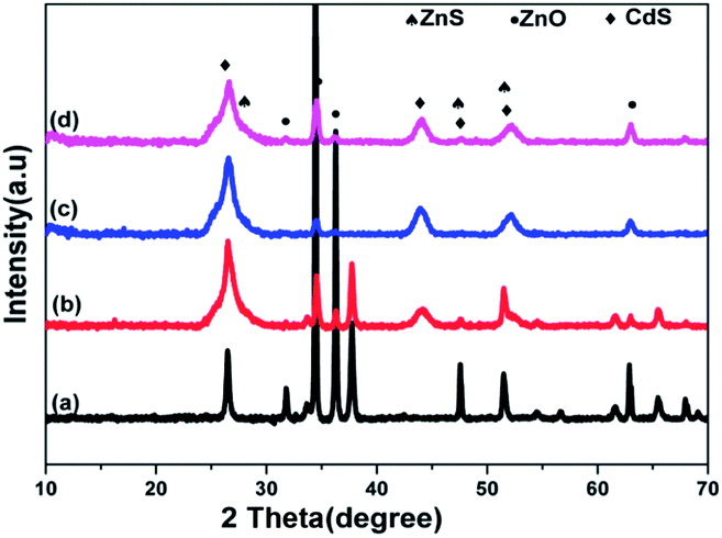 | ||
| Fig. 2 XRD spectra of ZnONRA (a), ZnONRA/CdS (b), ZnONRA/CdS/ZnS (c) and ZnONRA/ZnS/CdS (d). | ||
Fig. 3 shows UV-vis absorption spectra of ZnONRA/CdS, ZnONRA/CdS/ZnS and ZnONRA/ZnS/CdS. As is shown in Fig. 3a, ZnONRA/CdS has an absorption edge at ∼560 nm corresponding to the energy band gap value at about 2.24 eV. Compared with Fig. 3a, a slight blue shift can be observed in Fig. 3b after coating with ZnS. The blue shift is the result of a reaction between Cd2+ and S2− and/or the interdiffusion of Zn or Cd atoms at the CdS/ZnS interface during the annealing process.19 The absorption edge of ZnONRA/ZnS/CdS shows a slight red shift compared to ZnONRA/CdS. This could be explained by the presence of the ZnS buffer layer, which promotes the separation of photogenerated electron–hole pairs and extends the range of the excited spectrum.20
 | ||
| Fig. 3 UV-vis absorption spectra of ZnONRA/CdS (a), ZnONRA/CdS/ZnS (b) and ZnONRA/ZnS/CdS (c). | ||
EIS is an effective method to evaluate the photoelectrochemical properties of photocatalysts. EIS Nyquist plots are associated with the separation efficiency of the photogenerated electron–hole pairs and the charge transfer resistance.21 EIS measurements were carried out in the frequency range of 100 kHz to 0.1 Hz. Three semicircles with different radii can be observed in Fig. 4a. It is clear that the semicircles represent the complex charge transfer behaviour occurring at the photoelectrode, and the radii of curvature usually represent transfer resistance. It is important to note that a larger curvature radius corresponds to a larger charge transfer resistance and a lower separation efficiency for the photogenerated electron–hole pairs.22 The arc radii of the Nyquist plots in Fig. 4a show the EIS results for ZnONRA/ZnS/CdS, ZnONRA/CdS and ZnONRA/CdS/ZnS. Among the three EIS plots, ZnONRA/ZnS/CdS owns the smallest curvature radius resulting from the introduction of ZnS buffer layers; this is because ZnS buffer layers favour electron transfer and improve the separation efficiency of photogenerated electron–hole pairs. These analysis also explains why that curvature radius of ZnONRA/ZnS/CdS is smaller than that of ZnONRA/CdS. On the contrary, ZnONRA/CdS/ZnS has the biggest curvature radius, meaning that photogenerated electrons take longer to reach the FTO substrate. Fig. 4b shows the corresponding Bode phase plots of ZnONRA/CdS, ZnONRA/CdS/ZnS and ZnONRA/ZnS/CdS. Comparing the Bode phase plots shows that the characteristic peak of ZnONRA/ZnS/CdS shifts to a lower frequency when ZnS is introduced as a buffer layer. However, the characteristic peak position of ZnONRA/CdS/ZnS shifts slightly toward high frequency compared to that of ZnONRA/CdS. This is because the characteristic frequency is related to the inverse of the recombination lifetime or electron lifetime. ZnS buffer layers hinder the back electron transfer from the conduction band of ZnONRA to the redox couple, resulting a longer electron lifetime for the ZnONRA/ZnS/CdS photoelectrode. In other words, the characteristic frequency is related to the electron lifetime; a longer electron lifetime corresponds to a smaller frequency.
 | ||
| Fig. 4 Electrochemical impedance spectra of ZnONRA/CdS, ZnONRA/CdS/ZnS and ZnONRA/ZnS/CdS; (a) Nyquist plots and (b) Bode phase plots. | ||
Transient photocurrent response is generated by the transfer of excited photoelectrons from the valence band (VB) to the conduction band (CB), and mainly reflects the conductance value and the number of free photogenerated carriers in the semiconductor. The transient photocurrent responses of the ZnONRA/CdS ZnONRA/CdS/ZnS and ZnONRA/ZnS/CdS photoelectrodes are investigated for several on–off cycles of irradiation. As shown in Fig. 5, the photocurrent values rapidly decrease as soon as the light turns off, and the photocurrent comes back to a certain value when the light turns on. This phenomenon demonstrates that most of the photogenerated electrons migrate to the FTO substrates to yield photocurrent under visible light irradiation. In the present study, the transient photocurrent response of the ZnONRA/ZnS/CdS photoelectrode is the highest and that of ZnONRA/CdS/ZnS is the smallest. This result indicates a lower recombination rate and a more efficient separation of photogenerated electron–hole pairs for the ZnONRA/ZnS/CdS photoelectrode.
 | ||
| Fig. 5 Transient photocurrent response for the ZnONRA/CdS/ZnS, ZnONRA/CdS and ZnONRA/ZnS/CdS photoelectrodes. | ||
The photocatalytic hydrogen evolution over the ZnONRA/CdS, ZnONRA/CdS/ZnS and ZnONRA/ZnS/CdS photoelectrodes were evaluated using an aqueous solution containing Na2SO3 and Na2S as sacrificial reagents. The accumulated amount of evolved hydrogen and the average hourly hydrogen evolution as a function of irradiation time are shown in Fig. 6a and b, respectively. It can be clearly seen that the hydrogen generation rate over the ZnONRA/ZnS/CdS photoelectrode is the highest, and that over the ZnONRA/CdS/ZnS photoelectrode is the lowest. The average hydrogen evolution at each reaction time (1 h) was almost the same over the ZnONRA/ZnS/CdS (ca. 850 μmol) photoelectrode and the ZnONRA/CdS photoelectrode (ca. 620 μmol). However, the average hydrogen evolution over the ZnONRA/CdS/ZnS photoelectrode was lower (Fig. 6b). Meanwhile, the time-profiled photocurrent on the amount of H2 production during the photocatalytic water splitting reaction on the same time scale was investigated (Fig. S3†). The result demonstrates that the photocurrents on ZnONRA/ZnS/CdS and ZnONRA/CdS photoelectrodes were almost stable for 3 h, while the photocurrent on the ZnONRA/CdS/ZnS photoelectrode decreased during the photocatalytic water splitting reaction. The enhanced photocurrent and photocatalytic activity for hydrogen evolution over the ZnONRA/ZnS/CdS photoelectrode implies a more efficient separation of the photoinduced electron–hole pairs and a longer lifetime of the photogenerated charge carriers. Furthermore, the effect of ZnS buffer layers on the energy conversion is also confirmed in assembled ZnONRA/CdS, ZnONRA/CdS/ZnS and ZnONRA/ZnS/CdS solar cells (Fig. S4 and Table S1†).
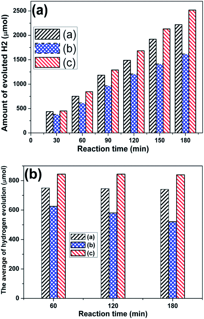 | ||
| Fig. 6 Time-profiled photocatalytic hydrogen evolution over ZnONRA/CdS (a), ZnONRA/CdS/ZnS (b) and ZnONRA/ZnS/CdS (c) in a homemade photoelectrochemical cell. | ||
ZnO, ZnS and CdS (Eg = 3.2, 3.6 and 2.4 eV, respectively) have different electron affinities and band configurations. ZnS has a higher conduction band edge with respect to ZnO, which is advantageous in the injection of excited electrons from ZnS (Scheme 2a). However, CdS has wider absorption band edges (below ca. 550 nm), and the electron injection efficiency is less than ZnS because its conduction band edge is located below that of ZnS. It has been reported that the photoelectrode of ZnO–CdS core–shell arrays have better charge separation and electron accumulation in the metal-semiconductor and semiconductor–semiconductor junctions than bare ZnO nanoarrays due to a shift of the Fermi level to a more negative potential.23 Pan et al. synthesized a heterostructured ZnO–ZnS nanocables photocatalyst via a template-assisted method. The coupled photocatalyst suggests that the higher photon efficiency and enhanced exciton separation lead to a remarkable enhancement (∼10 times) in photocatalytic activity compared to pure ZnO nanofibers.24 Liu et al. fabricated urchin-like ZnS/CdS semiconductor composites that exhibit enhanced photocatalytic degradation activities. The enhancement is attributed to the fact that the Fermi energy level of CdS is higher than that of ZnS. Thus, electrons in the VB of CdS were excited to its CB under light irradiation, and were then driven by potential energy to transfer to the CB of ZnS. Conversely, the photogenerated holes can move from the VB of ZnS to that of CdS. Consequently, the electrons and holes were separated efficiently at the ZnS/CdS interfaces, resulting in a large number of charges that could participate in the degradation reaction.25
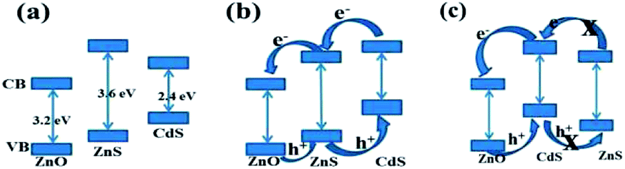 | ||
| Scheme 2 (a) Relative energy levels of ZnO, ZnS and CdS, (b) ideal stepwise band edge structure for the ZnONRA/ZnS/CdS photoelectrode, (c) the band edge structure for the ZnONRA/ZnS/CdS photoelectrode. | ||
To take advantages of two materials based on the above theory and our experimental results, CdS and ZnS were sequentially assembled onto ZnONRA, forming cascade structure photoelectrodes for the photoelectrochemical applications. The band gap will alternate when two different crystalline semiconductors (CdS and ZnS) are layered together with ZnONRA.26 We suspect that the enhanced photoelectrochemical activities of ZnONRA/ZnS/CdS may be related to the presence of ZnS buffer layers between the ZnONRA and CdS, which promote the separation efficiency of the photogenerated charge carriers, reduce the recombination probability of electrons and holes, and increase the charge carriers' lifetimes. Under visible light irradiation, electrons in the VB of CdS were excited to its CB, leaving holes at the VB position. As the Fermi energy level of CdS is higher than that of ZnS, the electrons in the CB of CdS were transferred to the CB of ZnS, followed by the potential energy-driven transfer to ZnO.25 On the contrary, the withdrawal of photoelectrons from the ZnS layer of the ZnONRA/CdS photoelectrode may cause space charge layer widening, causing the photogenerated electrons to take more time to reach the external circuit. Integrated ZnO, ZnS and CdS have synergistic effects on the photoelectrocatalytic activity,27 and ZnONRA as 1D nanostructures can supply a direct electron transport passageway, resulting in rapid electron transport to the external circuit. In our work, an enhanced rate of hydrogen production and a conversion efficiency as high as 0.88% were achieved with the ZnONRA/ZnS/CdS photoelectrode (Fig. S4 and Table S1†). However, a poor performance was obtained with the reversed structure, ZnONRA/CdS/ZnS. These results provide additional evidence to support the inference that Fermi level alignment between ZnS and CdS constructs a stepwise structure of band-edge levels in the ZnONRA/ZnS/CdS photoelectrode (Scheme 2b). which is advantageous to the charge transport and separation of electron–hole pairs in the CdS layer, and contributes to photoelectrode performance. On the contrary, the CB and VB of intermediate CdS will be higher than those of ZnS (Scheme 2c) in the ZnONRA/CdS/ZnS photoelectrode. In such an energy structure, the existing energy barriers inhibit the transfer of the excited electron from the ZnS to the CdS layer, which results in a low conversion efficiency for the ZnONRA/CdS/ZnS photoelectrode. The present work provides a new reference for the design and preparation of photocatalysts with higher efficiencies when utilizing visible light as an energy source.
4. Conclusions
The nanorod array photoelectrode of ZnO/ZnS/CdS was synthesized by depositing a thin layer of CdS and ZnS on the surface of ZnONRA using an alternative chemical deposition method. The ZnONRA/ZnS/CdS photoelectrode exhibits enhanced hydrogen production efficiency. The enhancement may be due to the presence of ZnS buffer layers, which would promote the separation efficiency of the photogenerated charge carriers and reduce the recombination probability for electrons and holes in the ZnONRA/ZnS/CdS photoelectrode.Acknowledgements
The work is supported by the Science & Technology Plan Project of Guangzhou City, China (No. 2013J4300035), the National Natural Science Foundation of China (No. 51172233) and the Foundation of the Key Laboratory of Water and Air Pollution Control of Guangdong Province (GD2012A05).Notes and references
- Q. Li, B. D. Guo, J. G. Yu, J. R. Ran, B. H. Zhang, H. J. Yan and J. R. Gong, J. Am. Chem. Soc., 2011, 133, 10878 CrossRef CAS PubMed.
- M. Grätzel, Nature, 2001, 414, 338 CrossRef PubMed.
- F. Yang, J. Y. Yao, F. L. Liu, H. C. He, M. Zhou, P. Xiao and Y. H. Zhang, J. Mater. Chem. A, 2013, 1, 594 CAS.
- B. Kannan, K. Castelino and A. Majumdar, Nano Lett., 2003, 3, 1729 CrossRef CAS.
- C. M. Chang, M. H. Hon and I. C. Leu, RSC Adv., 2012, 2, 2469 RSC.
- K. Ramanathan, M. A. Contreras, C. L. Perkins, S. Asher, F. S. Hasoon, J. Keane, D. Young, M. Romero, W. Metzger, R. Noufi, J. Ward and A. Duda, Prog. Photovoltaics, 2003, 11, 225 CAS.
- X. W. Wang, G. Liu, G. Q. Lu and H. M. Cheng, Int. J. Hydrogen Energy, 2010, 35, 8199 CrossRef CAS PubMed.
- Y. Tak, S. J. Hong, J. S. Lee and K. Yong, J. Mater. Chem., 2009, 19, 5945 RSC.
- I. Mora-Sero, S. Gimenez, F. Fabregat-Santiago, R. Gomez, Q. Shen, T. Toyoda and J. Bisquert, Acc. Chem. Res., 2009, 42, 1848 CrossRef CAS PubMed.
- K. Y. Yan, L. X. Zhang, J. H. Qiu, Y. C. Qiu, Z. L. Zhu, J. N. Wang and S. H. Yang, J. Am. Chem. Soc., 2013, 135, 9531 CrossRef CAS PubMed.
- G. L. Agawane, S. W. Shin, M. S. Kim, M. P. Suryawanshi, K. V. Gurav, A. V. Moholkar, J. Y. Leee, J. H. Yun, P. S. Patil and J. H. Kim, Curr. Appl. Phys., 2013, 13, 850 CrossRef PubMed.
- H. Lekiket and M. S. Aida, Mater. Sci. Semicond. Process., 2013, 16, 1753 CrossRef CAS PubMed.
- T. Nakada and M. Mizutani, Jpn. J. Appl. Phys., 2002, 41, 165 Search PubMed.
- K. Kushiya, Y. Tanaka, H. Hakuma, Y. Goushi, S. Kijima, T. Aramoto and Y. Fujiwara, Thin Solid Films, 2009, 517, 2108 CrossRef CAS PubMed.
- X. W. Wang, G. Liu, Z. G. Chen and F. Li, J. Mater. Res., 2010, 25, 39 CrossRef CAS.
- J. G. Jiang, M. Wang, L. J. Ma, Q. Y. Chen and L. J. Guo, Int. J. Hydrogen Energy, 2013, 38(29), 13077 CrossRef CAS PubMed.
- Y. Li, S. H. Li, L. Jin, J. B. Murowchick and Z. H. Peng, RSC Adv., 2013, 3, 16308 RSC.
- L. P. Wang, J. Li, S. H. Zhang, L. Z. Long, X. J. Li and C. P. Cen, J. Phys. Chem. C, 2013, 117(44), 22591 Search PubMed.
- X. N. Wang, R. Liu, T. Wang, B. Y. Wang, Y. Xu and H. Wang, ACS Appl. Mater. Interfaces, 2013, 5, 3312 CAS.
- R. S. Mane, W. J. Lee, H. M. Pathan and S. H. Han, J. Phys. Chem. B, 2005, 109, 24254 CrossRef CAS PubMed.
- S. N. Shen, U. KamachiMudali, G. Amarendra, P. Gopalan, R. K. Dayal and H. S. Khatak, Corros. Sci., 2006, 48, 1106 CrossRef PubMed.
- J. Y. Zheng, H. Yu, X. J. Li and S. Q. Zhang, Appl. Surf. Sci., 2008, 254, 1630 CrossRef CAS PubMed.
- D. R. Baker and P. V. Kamat, Adv. Funct. Mater., 2009, 19, 805 CrossRef CAS.
- D. D. Lin, H. Wu, R. Zhang, W. Zhang and W. Pan, J. Am. Ceram. Soc., 2010, 93(10), 3384 CrossRef CAS.
- S. L. Liu, H. L. Li and L. Yan, Mater. Res. Bull., 2013, 48, 3328 CrossRef CAS PubMed.
- V. Štengl and D. Králová, Int. J. Photoenergy, 2011, 1–14 Search PubMed.
- C. Calderón, J. S. Oyola, P. Bartolo-Pérez and G. Gordillo, Mater. Sci. Semicond. Process., 2013, 16, 1382 CrossRef PubMed.
Footnote |
| † Electronic supplementary information (ESI) available. See DOI: 10.1039/c4ra00005f |
| This journal is © The Royal Society of Chemistry 2014 |