Yun Ni*a,
Kai-lun Yaobc,
Chao-qun Tanga,
Guo-ying Gaob,
Hua-hua Fub and
Si-cong Zhub
aHuazhong University of Science and Technology, Wenhua College, Wuhan, China 430074. E-mail: niyun@hust.edu.cn
bSchool of Physics and Wuhan National High Magnetic Field Center, Huazhong University of Science and Technology, Wuhan, China 430074
cInternational Center of Materials Physics, Chinese Academy of Science, Shenyang 110015, China
First published on 4th March 2014
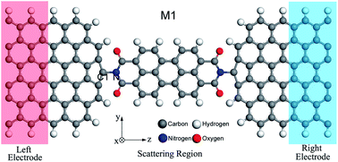
By performing first-principle quantum transport calculations, we proposed a multiple-effect organic molecular device for spintronics. The device is constructed of a perylene tetracarboxylic diimide molecule sandwiched between graphene electrodes. Our calculations show that the device has several perfect spintronics effects such as a spin-filter effect, a magnetoresistance effect, a negative differential resistance effect and a spin switching effect. These results indicate that our one-dimensional molecular device is a promising candidate for the future application of graphene-based organic spintronics devices.
It is well known that an infinite graphene sheet can be cut into two typical graphene nanoribbons (GNRs): armchair-edge GNR (AGNR) and zigzag-edge GNR (ZGNR).17,18 ZGNRs are more notable for their unique edge states and potential applications in spintronic devices such as spin-filter,19,20 spin-valve,21,22 giant magnetoresistance devices,23,24 and spin caloritronic devices.25,26 When the edges of ZGNRs are passivated by hydrogen atoms, they have three magnetic states: the non-magnetic (NM) state, the ferromagnetic (FM) state and the anti-ferromagnetic (AFM) state. It has been reported that ZGNR-H has a magnetic insulating ground state with an AFM state,18 and can be magnetized by applying a sufficiently strong magnetic field, leading to a FM state.9,23 Recently, R. N. Mahato et al. announced that they found an exceptionally large, room-temperature, small-field magnetoresistance (MR) effect experimentally in a one-dimensional organic molecular wires system.27 In addition, the organic molecular wires were composed of perylene tetracarboxylic diimide (PTCDI) derivatives, and the confinement of current path in molecular systems can lead to a strong increase of the MR. As we know, PTCDI and its derivatives play a role in industry as red to brown dye pigments, and show good n-conducting properties when used as organic semiconductors,28,29 which makes them attractive for organic spintronics.
In this paper, we numerically investigate the spin-resolved electron transport for a one-dimensional molecular device, where the PTCDI molecule is sandwiched between two ferromagnetic ZGNR electrodes. Since the spin orientation of the ZGNR electrodes can be adjusted by an external magnetic field,20,30,31 the magnetization configuration of the device can be set to a parallel configuration (PC, the spin orientation of both the left and right electrodes is up) and an antiparallel configuration (APC, the spin orientation of the left electrode is up and the right one is down). We found that in the PC configuration the spin-up transport channel is open while the spin-down one is closed at the Fermi level. This can reach 100% spin polarization and is ideal for spin filters. Moreover, the device shows an obvious negative differential resistance (NDR) effect and a very large MR. In addition, we can observe an obvious switching effect by changing the orientation of the PTCDI and ZGNR planes.
Our first-principles calculations are based on the ATOMISTIX TOOLKIT (ATK) package,32–34 which adopts spin density functional theory combined with a nonequilibrium Green's function.35,36 The core electrons are described by norm-conserving pseudopotentials, and the local-density approximation (LDA) is used for the exchange-correlation potential.9,18,37 A single-polarized (SZP) basis set is used and the cutoff energy is 150 Ry. A Monkhorst-Pack k-mesh of 1 × 1 × 100 is chosen in our work. The structure was optimized before calculation. According to the optimization, the bond distance of the C1 and N atoms is about 1.43 Å, which is close to the length of a carbon–nitrogen single bond, so we believe that the covalent bond type of the C1 and N atoms is a σ-bond. The convergence parameters of the optimization were chosen as follows: total energy tolerance 1 × 10⁻⁵ eV per atom, and maximum force tolerance 0.05 eV Å−1. The vacuum layers between two sheets along the x and y directions (defined in Fig. 1) are more than 10 Å. The NEGF-DFT self-consistency is controlled by a numerical tolerance of 10−5 eV. The integration grid of the current calculation is 10 × 10. The spin-dependent current through the system is calculated using the Landauer formula:
![]() | (1) |
T↑(↓)(E) = Tr[ΓLGRΓRGA]↑(↓), | (2) |
From the spin-resolved I–V curves of our device from 0 to 0.2 V in different magnetization configurations (Fig. 3a), we can also find some singular points, like the 0.18 V of the PC and the 0.15 V of the APC for the spin-up currents. We would like to take the spin-up one in the PC case as an example to explain the cause of the singular point. The inset of Fig. 3a shows the detail of the current curve in the vicinity of 0.18 V. We can see that the current suddenly drops at 0.175 V, and then the curve stays low and changes very little until 0.186 V, where the current sharply increases and remains high. As we know, the transport properties of a molecular device are determined by the electronic structures of the molecules, especially the energy positions of the molecular orbitals, which provide transmission channels for electron tunneling. In order to see the variation in the molecular orbitals more clearly, we plotted the bias-dependent evolutions of the LUMO (lowest unoccupied molecular orbital), the HOMO (highest occupied molecular orbital), the LUMO + 1 and the HOMO − 1. Since the molecular orbitals are similar in the bias voltage range from 0.175 V to 0.185 V, we take the case of 0.18 V as the representative voltage. As shown in Fig. 3d, the energy was chosen to be from −0.3 eV to 0.3 eV, the triangular region surrounded by the intersecting dashed lines is referred to as the bias window, and the energy data are molecular projected self-consistent Hamiltonian (MPSH) eigenvalues. As we know, only the energy levels located in the bias window contribute to the transport. It can be clearly seen that the HOMO–LUMO gap decreases gradually with an increasing bias from 0 V to 0.15 V, so the current rises linearly and stably in this region. When the bias reaches 0.16 V, although the HOMO–LUMO gap does not obviously change, the HOMO orbital rises and is very close to the Fermi level, resulting in a large increase of the current at 0.16 V (Fig. 3a). At 0.18 V, the current suddenly drops and this can be explained by the molecular orbitals shown in Fig. 3d. The LUMO orbital at 0.18 V ascends with a major step, not only greatly increasing the HOMO–LUMO gap, but also going beyond the region of the bias window. Meanwhile, the HOMO-1 orbital enters the bias window, but the MPSH eigenstates for the HOMO-1 at 0.18 V (Fig. 3e) shows that they are highly localized at the right electrode area and do not contribute to the electron transport. Therefore, the current around 0.18 V (from 0.175 V to 0.185 V) is very small in the spin-up I–V curve of the PC. For the spin-down case and the APC configuration, the variation of the I–V curves can also be analyzed in the same way.
Also, we investigate the magnetoresistance (MR) of the device when changing from the PC to the APC magnetization configuration, which can be obtained from the equation MR (%) = (RAP − RP)/(RP) × 100, where RAP and RP are the resistances in the APC and PC configurations. Note that when the bias is zero, the MR can be calculated by the transmission coefficient of the spin-up and spin-down electrons in the PC and the APC, which is MR (%) = [(TAP-up + TAP-down)−1 − (TP-up + TP-down)−1]/(TP-up + TP-down)−1 × 100. With a non-zero bias, the MR is obtained from the total current of the PC and the APC, which is MR (%) = [(IPC − IAPC)/IAPC] × 100. Fig. 4a shows the bias-dependent MR of the device. The maximum value of the MR occurs at zero bias and is nearly 104%, yet it decreases quickly with a rise in the bias. With a small bias, when the bias reaches 0.1 V, the MR drops to about 103%, which is still larger than that of conventional metal-based MR devices. The large MR effect is mainly caused by the selective transmission of the spin-resolved electrons in the device, and is very significant for the fabrication of efficient graphene-based spin-valve devices.
![]() | ||
Fig. 4 (a) The magnetoresistance of the device. (b) The spin-resolved I–V curves for the PC and the APC configurations with a bias up to 1.0 V. |
Next, we investigate the spin-resolved currents at a larger bias (less than 1.0 V), and the corresponding I–V curves are shown in Fig. 4b. It can be clearly seen that both in the PC and the APC configurations the currents are spin-polarized, and the spin-polarization of the PC is generally larger than the APC. It is noteworthy that some of the curves show obvious NDR effects, among which the spin-up one of the PC configuration is the most significant. Thus with this case as the representative case, we will thoroughly investigate the formation mechanism of the NDR effect. First, we present the spin-up transmission spectra around the Fermi level in Fig. 5, with the bias selected in the range from 0.3 V to 0.8 V since the NDR effect occurs mainly within this region. The comparison of the transmission spectra at biases of 0.3 V and 0.7 V shows that with the bias window expanding the spin-up spectrum varies greatly. The peak above the Fermi level shrinks and shifts away from the Fermi level, and in the spectrum below the Fermi level a sharp peak at about −0.15 eV gradually appears. From eqn (1), we know that the current is determined by the corresponding integral areas of the transmission spectra in the bias window. However, we can't judge the values of the integral areas at 0.3 V and 0.7 V intuitively, since the variation of the spectra is quite complex. In order to see the cause of the NDR effect more intuitively, we have investigated the bias-dependent evolutions of several molecular orbitals near the Fermi level, and the MPSH eigenvalues are shown in Fig. 6a. It can be clearly seen that when the bias reaches 0.4 V, the HOMO descends but the LUMO ascends, leading to a dramatic increase of the HOMO–LUMO gap. Simultaneously, as seen from the MPSH eigenstates of the HOMO and LUMO orbitals at biases of 0.3 V and 0.4 V (Fig. 6b–e), the distribution of the HOMOs are almost the same throughout the PTCDI molecule providing the channels for transmission. However for the LUMOs, the MPSH eigenstates at a bias of 0.4 V are more localized than at 0.3 V. This is why the NDR effect occurs at 0.4 V. When the bias reaches 0.7 V, the current curve is in a valley and then it rises rapidly at 0.8 V. As shown in Fig. 6a, from 0.7 V to 0.8 V, both the HOMO and the LUMO descend, and the LUMO at 0.8 V is located very close to the Fermi level despite the slight increase of the HOMO–LUMO gap. Meanwhile we can also observe the MPSH eigenstates of the HOMO and the LUMO at biases of 0.7 V and 0.8 V (Fig. 6f–i). The distributions of the HOMOs are throughout the PTCDI molecule at both biases, but the LUMOs are quite different. The LUMOs are quite localized at the right electrode at a bias of 0.7 V, but distributed throughout the centre region at 0.8 V, so the current rises significantly when the bias goes from 0.7 V to 0.8 V.
![]() | ||
Fig. 5 The spin-dependent transmission spectra of the device at biases of (a) 0.3 V, (b) 0.4 V, (c) 0.5 V, (d) 0.6 V, (e) 0.7 V and (f) 0.8 V in the PC configuration. |
Finally, we consider another configuration of the PTCDI molecule and the GNR leads, which is shown in Fig. 7 and defined as M2. The orientation of the PTCDI plane is perpendicular to the ZGNR, which may be changed from the M1 configuration (Fig. 1) by thermal activation, by micromechanical operation or by an electric field.38–41 The calculated spin-dependent currents of M1 and M2 both in the PC and the APC are shown in Fig. 8a and b, where we can see clearly that the currents of M2 are smaller when compared with those of M1. That is to say, the spin-resolved currents can be controlled by changing the orientation between the planes of the PTCDI molecule and the GNR leads. When the planes are coplanar, the molecular device is on; when the planes are perpendicular, the molecular device is off. The corresponding ON/OFF switch ratios are displayed in Fig. 8c and d. For most biases up to 1.0 V, the ON/OFF ratios are dramatically high, and the highest reaches 105 for the spin-up condition at 0.2 V in the APC. The ratios are quite large but not steady, which needs to be improved further. The huge ratio is caused by the mismatch between the py channel of the PTCDI molecule and the π-orbital of the GNR in the perpendicular configuration, resulting in nearly no channels for electron transmission. This outstanding switching effect makes the device a possibility for achieving an ideal spin switching device, and this plays an important role in the application of spintronics.
![]() | ||
Fig. 7 Schematic of the switching device when the orientation of the PTCDI plane is perpendicular to the ZGNR plane. |
![]() | ||
Fig. 8 The spin-resolved I–V curves for M1 (ON) and M2 (OFF) in (a) the PC and (b) the APC configurations. (c and d) ON/OFF switch ratios in the PC and the APC. |
This journal is © The Royal Society of Chemistry 2014 |