Computational modelling and characterisation of nanoparticle-based tuneable photonic crystal sensors

Constantinos P. Tsangarides a, Ali K. Yetisenb, Fernando da Cruz Vasconcellosb, Yunuen Montelongoa, Malik M. Qasima, Timothy D. Wilkinsona, Christopher R. Loweb and Haider Butt*c
aElectrical Engineering Division, Department of Engineering, University of Cambridge, Cambridge, CB3 0FA, UK
bDepartment of Chemical Engineering and Biotechnology, University of Cambridge, Tennis Court Road, Cambridge, CB2 1QT, UK
cSchool of Mechanical Engineering, University of Birmingham, Edgbaston, Birmingham B15 2TT, UK. E-mail: h.butt@bham.ac.uk

Received 26th December 2013 , Accepted 4th February 2014

First published on 4th February 2014


Abstract

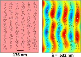
Photonic crystals are materials that are used to control or manipulate the propagation of light through a medium for a desired application. Common fabrication methods to prepare photonic crystals are both costly and intricate. However, through a cost-effective laser-induced photochemical patterning, one-dimensional responsive and tuneable photonic crystals can easily be fabricated. These structures act as optical transducers and respond to external stimuli. These photonic crystals are generally made of a responsive hydrogel that can host metallic nanoparticles in the form of arrays. The hydrogel-based photonic crystal has the capability to alter its periodicity in situ but also recover its initial geometrical dimensions, thereby rendering it fully reversible and reusable. Such responsive photonic crystals have applications in various responsive and tuneable optical devices. In this study, we fabricated a pH-sensitive photonic crystal sensor through photochemical patterning and demonstrated computational simulations of the sensor through a finite element modelling technique in order to analyse its optical properties on varying the pattern and characteristics of the nanoparticle arrays within the responsive hydrogel matrix. Both simulations and experimental results show the wavelength tuneability of the sensor with good agreement. Various factors, including nanoparticle size and distribution within the hydrogel-based responsive matrices that directly affect the performance of the sensors, are also studied computationally.


Introduction

Photonic crystals (PC) have applications in a myriad of applications such as optical devices, sensing materials and display technologies.1 We studied the optical tuneability of one-dimensional (1D) photonic crystals, also known as Bragg mirrors. The mechanism behind the operation of photonic crystals is governed by the periodicity of their lattice anatomy, which can directly affect the propagation of photons. Periodicity in lattices represents an alternating pattern of macroscopic dielectric media along a specific direction.2,3 If the absorption of light by the entire structure is minimal, and there is a large contrast between the dielectric strength of the alternating media, some frequencies are filtered out as they pass through the media. The excluded group of frequencies is called the photonic band gap (PBG). A wide array of optical applications have been devised, which utilise the band gaps of photonic crystals, such as Fabry–Perot filters, distributed feedback lasers (DFBs),4 reflective coatings for sunglasses or aircraft windows and anti-reflective coatings for light-emitting diode (LED) enhancement of output efficiency.5 Photonic crystals can also be used as waveguides,6,7 wavelength multiplexers8 and colour filters.9 All of these devices have a wide range of commercial applications from telecommunications based on optical fibres and routing to medical fields for sensing and quantitative analyses.10

Photonic crystal-based dynamic structural coloration in nature is rare. Notable examples include fish (e.g. Paracheirodon innesi),11,12 cephalopods13 and beetles (e.g. Tmesisternus isabellae).14,15 The diversity of photonic structures might provide camouflage, warning colouration, superiority in reproductive behaviour, signal communication, thermoregulation and conspecific recognition. The dynamic coloration is generally achieved by altering the dielectric structure either by changing the thickness of the multilayers or the refractive index of individual layers through chemical reactions. The operational mechanism for these naturally occurring tuneable photonic crystals may seem quite simple, but difficulties arise in the fabrication of such structures in the laboratory. A photonic crystal is constructed according to the frequency range that the PBG must fall in. If infrared frequencies are required, micron dimensions must be used for a given geometry.4 The higher the frequency band the smaller must be the photonic crystal structure. Hence, for the visible region, which is the main interest of this study, the fabrication is challenging and costly. Most typical strategies to fabricate a 1D geometry photonic crystal are based on either molecular beam epitaxy (MBE)16 or chemical vapour deposition (CVD).17 However, MBE is a slow and expensive process, while CVD lacks positional precision and compatibility with several notable materials.18–24 Consequently, they do not fulfill the desired attributes for mass production capability and practical applications via low cost, and material and process flexibility.

A rapid, low-cost and efficient approach is to develop a PBG structure through creating a periodic structure via laser light.25 It has been demonstrated recently that the light-directed fabrication of 1D photonic crystal structures in functionalised media allow tuning their PBG in response to external stimuli.25 The photonic crystals therefore act as chemical sensors. The materials used to construct these photonic crystals were composed of a functionalised hydrogel and metallic silver nanoparticles; the resulting polymer was both transparent and elastic. The silver nanoparticles were organised within the hydrogel in particular formations (via laser photochemical patterning) such that it produces a periodicity through the thickness of the hydrogel (see ESI for electron micrographs).

The nanoparticle-based multilayered structure that was formed within the hydrogel acts as a 1D photonic crystal, which diffracts the frequencies of electromagnetic radiation that fall within the band gap region. When the band gap region shifts its position to higher or lower frequencies, different frequencies are back scattered. The functionalised hydrogels used as the medium for the multilayered structures have the ability to vary their thickness in response to chemical stimuli. For example, this may be achieved via protonation and deprotonation of carboxyl groups in pH-sensitive hydrogels. Altering the thickness of the hydrogel directly changes the lattice constant of the photonic crystal periodicity and therefore induces a band gap shift.

Here we demonstrate a theoretical and experimental study of a 1D photonic crystal-based tuneable sensor. A photonic crystal sensor sensitive to pH changes was fabricated using laser-directed photochemical patterning. Computational simulations are utilized to analyze the tuneability and optical characteristics of the photonic sensor to achieve further improvements in the fabrication procedure.

Modelling of photonic crystal sensor

To present the working principle of the PC sensor, we used a finite element method based computational software, COMSOL Multiphysics®.26 The photonic crystal consisted of periodic layers of nanoparticles in a hydrogel medium. The photonic crystal patterns consisting of stacks of randomly sized nanoparticles were generated using a MATLAB code. Since the hydrogel medium has a refractive index of 1.512, and the laser wavelength used for photochemical patterning was λ = 532 nm, then λ/2n would give a lattice constant of l = 176 nm to the nanoparticle-based multilayered structure. As shown in Fig. 1, the 1D periodic array of stacks consisted of nanoparticles designed as nanospheres with different radii.
image file: c3ra47984f-f1.tif
Fig. 1 A simulated geometry of a photonic crystal (a) model geometry showing silver nanoparticle stacks within a hydrogel medium. (b) Meshing of the silver nanoparticle pattern.

As a starting point, the number of nanospheres tested per stack was ∼60, with 6 stacks in total. Along the vertical axis of each stack, the nanospheres were uniformly distributed, whilst in the horizontal axis, the nanospheres were distributed within the layers defined by the laser-induced photochemical patterning. To achieve this, a normal random distribution was performed with the mean positions of the stacks set with a distance equal to the lattice constant. Additionally, to render the photonic pattern more realistic in terms of representing a fabricated photonic multilayer system, a normal random distribution was also used to define the radii of the nanospheres. The mean value of the radii was set within a range from 4–24 nm, σ = 5 nm.

After generating the nanoparticle patterns in MATLAB, they were imported into COMSOL for two-dimensional (2D) modelling. The pattern of nanospheres was then surrounded with a square domain of a medium that mirrored the material of the hydrogel to have a refractive index of 1.512. The remaining subdomains (i.e. nanospheres) were set to have an electrical conductivity of silver (61.6 mS m−1). Since there is an absorption of electromagnetic radiation by the silver nanoparticles, a complex refractive index was required. This absorption should not affect significantly the propagation of light when taking into account a small number of stacks. However, the absorption can reduce the efficiency of diffracted light when considering photonic crystals that have a high number of stacks. Fig. 1 shows how the photonic crystal was represented when fully constructed in the COMSOL Multiphysics® software. The electromagnetic waves were incident on the photonic crystal from the left and propagated from left to right along the array of nanoparticle stacks. The left boundary of the cell was set to a scattering boundary condition. The light source was defined as a plane wave of varying wavelengths obeying by the following equation:26

 
n × (∇ × Hz) − jkHz = −jk(1 − k·n)Hoz[thin space (1/6-em)]exp(−jkr) (1)
where, n is the complex refractive index, Hz is the magnetic field strength at position r, k is the propagation constant and Hoz is the initial magnetic field strength. Meshing was performed with the smallest finite element size of ∼2 nm to resolve each nanoparticle. Once meshing was established, a computation was performed via a parametric sweep, providing the ability to solve for a range of wavelengths in a single simulation run. The wavelength parameter values set covered a range from 400 nm to 900 nm within the entire visible spectrum. Finally, using “power outflow and time average” boundary integration, the relevant data of transmission of the waves was collected. By analysing the results, the amount of radiation reaching the opposite end of the photonic crystal can be estimated.

Simulation results

Fig. 2 shows the simulated optical transmission results for the photonic crystal. Fig. 2(d) illustrates the transmission spectrum for the PC. The spectrum shows peak reflectivity at ∼532 nm, corresponding to the wave propagation for a lattice spacing of 176 nm, shown in Fig. 2(a). This is the wavelength that undergoes lowest transmission due to Bragg diffraction, which defines the green diffracted colour of the photonic crystal system. This demonstrates that the colour of the photonic multilayer device is dictated by the spacing between the nanoparticle stacks.
image file: c3ra47984f-f2.tif
Fig. 2 Model geometries and wave propagation results for the Bragg diffracted waves for photonic multilayer structures with lattice constants of (a) 176 nm, (b) 215 nm and (c) 270 nm. (d) The simulated transmission spectra for different photonic crystal lattices. A red shift in the reflection bands was observed with the increase in lattice constants.

Additional simulations were performed to analyse the effect of expanding the nanoparticle lattice on the reflection band gaps. Here, the photonic multilayer structure was expanded, while keeping the number and dimensions of the nanoparticles constant, simulating the tuneable nature of a hydrogel-based photonic crystal device. Tuneable hydrogel-based systems are functionalised and tailored to respond to an external stimulus, such as a pH change. This response results in a corresponding shrinkage or expansion of the hydrogel, and hence, of the multilayered lattice within it. As shown in Fig. 2(b) and (c), the lateral expansion of the photonic crystal system results in an increase in the effective-stack spacing, stack size and a reduction in the concentration of nanoparticles per stack. The overall effect of these changes on the wave propagation was clearly observed in the simulated transmission results. The transmission spectra (Fig. 2(d)) show a red shift in the reflection bands with an increasing stack spacing. The expanding multilayer structure displayed a changing colour (reflection band) varying across the visible spectrum from approximately 532 nm to 815 nm. It was also observed that with an increase in stack spacing, the efficiency of the multilayer structure decreases, shown by the decrease in the intensity of the reflection band. This could be due to the decrease in the concentration of nanoparticles present in each stack, which reduces the effective index contrast between the nanoparticle stacks and the surrounding medium.

PC sensor fabrication

Based on the working principle of a tuneable 1D PC (as demonstrated in the simulated results), a pH-sensitive photonic crystal sensor was fabricated. The PC sensor consisted of a poly(2-hydroxyethyl methacrylate) (pHEMA) film (∼10 μm thick) on a glass substrate. First, the glass substrate was treated with 3-(trimethoxysilyl)propyl methacrylate in acetone 1[thin space (1/6-em)]:[thin space (1/6-em)]50 (v/v) to promote adhesion of the methacrylate polymer to the substrate (Fig. 3(a)). A monomer solution (200 μl) consisting of 2-hydroxyethyl methacrylate (HEMA) (91.5 mol%), ethylene dimethacrylate (EDMA) (2.5 mol%), and methacrylic acid (MAA) (6 mol%) was prepared. The solution was mixed by 1[thin space (1/6-em)]:[thin space (1/6-em)]1 (v/v) with 2% (w/v) 2-dimethoxy-2-phenylacetophenone (DMPA) in propan-2-ol and the resulting solution was polymerised on the silanised glass substrate using UV light-induced free radical polymerisation for an hour (Fig. 3(b)). The resulting pHEMA and glass substrate system was rinsed with ethanol (100%) in order to remove unreacted compounds (Fig. 3(c)).
image file: c3ra47984f-f3.tif
Fig. 3 Fabrication of a photonic crystal sensor via silver halide chemistry. (a) A glass slide was functionalised with silane chemistry; (b) the monomer mixture was polymerised on the glass slide; (c) the resulting system was rinsed with ethanol; (d) a AgClO4 solution was allowed to diffuse into the polymer; (e) the excess AgClO4 solution was removed and the system was dried; (f) silver halide grains were formed in the pHEMA film; (g) the system was rinsed with DI water; (h) the system was exposed to a single pulse of a laser-light at 5°; (i) the latent image was developed to metallic silver; (j) the system was neutralised; (k) undeveloped silver halide grains were removed from the system; and (l) the system was rinsed with ethanol solution in order to remove the cyanine dye from the hydrogel matrix.

Under red safe lighting, an AgClO4 solution (200 μl, 0.3 M) dissolved in propan-2-ol and DI water (1[thin space (1/6-em)]:[thin space (1/6-em)]1, v/v) was allowed to perfuse into the polymer layer for 3 min (Fig. 3(d)). The excess AgClO4 solution was removed with a squeegee and the film was dried under a tepid air current for 5 s (Fig. 3(e)). For 30 s, the pHEMA–glass system was submerged into a photosensitising bath, which consisted of lithium bromide (0.3 M, 40 ml) in 3[thin space (1/6-em)]:[thin space (1/6-em)]2 (v/v) methanol[thin space (1/6-em)]:[thin space (1/6-em)]H2O and 1,1′-diethyl-2,2′-cyanine iodide (1[thin space (1/6-em)]:[thin space (1/6-em)]500, w/v, 1 ml) in methanol (Fig. 3(f)). The slide was washed thoroughly with deionised (DI) water (Fig. 3(g)).

Once the photosensitisation was achieved, the system was exposed to laser light and developed. A levelled Petri dish, with a mirror placed on the bottom surface, was filled with unbuffered ascorbic acid (2%, w/v) (pH 2.66). Polymer side facing down, the slide was immersed in the bath with an inclination of 5°. The polymer film was equilibrated in the bath for 15 min. Next, the film was exposed to a single 6 ns pulse by Nd–yttrium–aluminum–garnet (Nd:YAG) laser (350 mJ) with a spot size larger than the pHEMA–glass system (Fig. 3(h)). A photographic developer (pH 13.0) comprising of 4-methylaminophenol sulphate (0.3%, w/v), ascorbic acid (2%, w/v), sodium carbonate (5%, w/v) and sodium hydroxide (1.5%, w/v) was dissolved in DI water. The film was submerged in the developer until no more darkening was seen (Fig. 3(i)). The film was washed thoroughly with DI water and immersed in acetic acid (5%, v/v) solution to neutralise the developer (Fig. 3(j)). The film was rinsed with DI water and immersed in 10% (w/v) sodium thiosulphate mixed with ethanol 1[thin space (1/6-em)]:[thin space (1/6-em)]1 (v/v) for 15 min to remove the undeveloped lithium bromide grains (Fig. 3(k)). Finally, the film was submerged in an ethanol–water (50% v/v) solution for 15 min to remove the cyanine dye from the polymer matrix and this process was repeated three times (Fig. 3(l)). The result is a 1D photonic crystal consisting of silver nanoparticles layers within a dynamic hydrogel medium. Similar multilayer structures have also been reported earlier using this method (see ESI).

Experimental results

Photonic crystal sensor response

Optical measurements were performed on the fabricated pH-sensitive photonic crystal sensors. Buffer solutions (150 mM) consisting of Na2HPO4–citric acid (pH 3.00–8.00), Na2HPO4–HCl (pH 9.00), Na2HPO4–NaOH (pH 10.00) were prepared to obtain the desired pH values. The sensor (0.5 cm × 2.5 cm) was first submerged into a cuvette and buffers in the range of pH 3.00–10.00 were dispensed into the reservoir. The cuvette was centred in a goniometer setup having a white light source and spectrometer. The reflection spectra from the PC sensor were measured using the spectrometer. A bifurcated cable was used to feed the spectral data into a camera as well to capture images corresponding to the spectrometer measurements. Fig. 4(a) shows the measurements of reflection spectra of the pH-sensitive photonic crystal sensor. With the increase in pH, the hydrogel expands, which consequently increases the lattice spacing between the silver nanoparticle layers. The reflection spectra was red shifted by ∼280 nm, which was predicted by the simulation results. An increase in lattice spacing consequently reduced the effective index contrast, hence the efficiency of the multilayer structure decreased, also predicted by the simulations. The tunable wavelength shift as a function of pH is shown in Fig. 4(b) After every reading, the pH buffer was removed and the cuvette flushed consecutively three times for each new buffer point. A standard error bar in the Fig. 4(b) represents three replicates of the same sensor. Standard error bars in pH were approximated using linear interpolation based on the calibration curve. The apparent pKa value was calculated as 6.08 using the Henderson–Hasselbalch equation. Fig. 4(c) shows the camera images (colour readouts) for the PC sensor showing different colours diffracted in the presence of different pH values. The sensors operated within the visible spectrum as well in the near infrared. The spectrophotometer has a resolution of 0.5 nm wavelength shift, which corresponds to a minimum fringe swelling distance of 0.18 nm, which obeys the Bragg's law (λpeak = 2nd[thin space (1/6-em)]cos(θ)), where λpeak is the wavelength of the first order diffracted light at maximum intensity, n is the average effective refractive index, d is the lattice spacing between the two consecutive layers, and θ is the angle of incidence of the incoming illumination. Since a ∼10 μm thick hydrogel was fabricated in this study, it can theoretically accommodate ∼55 fringes. In order to cause a resolvable spectral shift, the hydrogel needs to swell a minimum of ∼9.7 nm.
image file: c3ra47984f-f4.tif
Fig. 4 (a) Visible-near-infrared diffraction spectra of a photonic crystal sensor swollen by different pH solutions using phosphate buffers. (b) The sensor response over three trials. The measured wavelength shifts in the reflection spectra. (c) Colorimetric readouts of the photonic crystal sensor at various pH, taken using a CCD camera.

The pH-sensing range and the sensitivity of the sensor can be controlled through variation of the nature of the ionisable co-monomer in the polymer matrix and its concentration.27 The sensor can also be synthesised to respond to other analytes such as glucose,28 metal ions29 and hormones.30

Simulations of other parameters

Further simulations were also carried out to study different parameters that could influence the performance of the presented PC sensor. This analysis will be helpful to optimise the fabrication of the current photonic crystal structures.

Effect of mean nanoparticle size

The effect of varying nanoparticle radii on the performance of the photonic crystal was evaluated. Nine different geometries were generated with a range of mean nanoparticle radii from 6 nm to 22 nm. The number of nanoparticles per stack was kept constant at 60. The transmission plots in Fig. 5 show that as the nanoparticle size increases, so does the intensity of the reflection band, which can be attributed to the area that these respective nanoparticles with varying sizes cover. It was stated in the previous simulation run that a higher effective refractive index of the stack will give a stronger reflection. Therefore, if all these configurations have the same number of particles, then those with larger particles will cover more area within the hydrogel medium, thus resulting in a higher effective refractive index. The disadvantage, however, of having a photonic structure with very large nanoparticles, is that these particles induce a very broad bandwidth and a redshift on their reflection band gap.
image file: c3ra47984f-f5.tif
Fig. 5 Simulated transmission for a variety of patterns consisted of silver nanoparticles of lattice constant 176 nm but different mean radius size. Large nanoparticle mean radius sizes lead to broader stop bands centered at longer wavelengths.

The broad bandwidth can be explained by the uneven uniformity in the width of the stacks in a photonic crystal pattern. For example, for r = 22 nm, not all five stacks have the same width, because MATLAB attempted to generate a pattern where the nanoparticles were evenly spaced inside a stack and hence placed them with a modest degree of uniformity along the horizontal direction. The red shift can also be explained by the surface plasmonic resonances of the silver nanoparticles.31 The excitation of surface plasmons arises from the excitation of a collective electron oscillation within the nanostructure induced by the incident light. This leads to a large optical local-field enhancement and a dramatic wavelength-selective photon scattering and localisation at the nanoscale. The plasmonic resonances are highly affected by the size, shape and the medium of silver nanoparticles. The reflected light/band gaps displayed by the PC sensor were highly influenced by the plasmonic resonance of the silver nanoparticles. As the average nanoparticle size increased, the peak plasmonic resonance underwent a red shift. Therefore, the band gaps broadened as they represent an effective reflection, which occurred due to the periodicity of the stacks and the surface plasmon resonances of the large silver particles.

The ideal radius size should be between 8 nm and 10 nm even if they seem to give weaker reflections than the larger size particles. In this range, the surface plasmon resonance and the lattice constant dictated band gaps seem to coincide. The reflection intensity can also be improved by increasing the concentration of the particles as discussed later.

Effect of number of nanoparticle stacks

The effect of changing the number of nanoparticle stacks was also studied. As shown in Fig. 6(a)–(c), three configurations were simulated, with all consisting of 60 nanospheres per stack with a mean radius of 10 nm and a lattice constant of 182 nm. Fig. 6(d) shows the transmission plots respectively for all configurations. All curves show a transmission dip at 550 nm. This shows that the reflection band does not change position by adding or removing stacks of silver nanoparticles with the same periodicity. By looking at the depth of each trough it can be clearly seen that, as the number of stacks increases, so does the intensity of the reflected diffraction. For 6 stacks, there is a 60% reflection (0.4 normalised transmission), for 5 stacks there is a 48% reflection and for 4 stacks a 40% reflection. Therefore, at 6 stacks the reflection seems to be stronger than other two. It is also observed that the lower the reflection, the wider the trough appears to be. The full width at half maximum (FWHM) of the 4 stacks curve is 160 nm, whereas in a 6 stack it is 110 nm. Consequently, the greater the number of nanoparticle stacks, the deeper the PBG trough and narrower the bandwidth become.
image file: c3ra47984f-f6.tif
Fig. 6 Simulations were performed with (a) 4 stacks, (b) 5 stacks and (c) 6 stacks of silver nanoparticles, with a lattice constant of 182 nm. The wave propagation results are shown for the wavelength of 550 nm in each case. (d) Each curve represents the transmission along the patterns with the corresponding number of stacks. All of them show a stop band centered at 550 nm, however with varying depth.

Effect of the number of nanoparticles per stack

Four different configurations were used with varying numbers of nanoparticles per stack, ranging from 20 to 80 nanoparticles per stack (Fig. 7). Comparing the model geometries, we can observe that as the number of nanoparticles per stack increases, the stacks become more uniform; like a continuous medium with fewer voids. This means that the effective refractive index of the stacks is different in each case. As shown in the spectral results (Fig. 7), the case with 20 particles per stack gives very weak reflection. With an increasing number of particles the reflection band becomes stronger, with the deepest one reaching 65% of reflection for 80 particles per fringe. Increasing the number of particles increases the index contrast between the layers with and without the nanoparticles, thus resulting in lower reflection. Also with the increase in the number of nanoparticles the net absorption increases leading to effectively lower transmission. By carefully observing the position of the trough it seems that it undergoes a red shift with the increase in particles per stack. At 20 particles per stack, the minimum point of the curves are located near 530 nm, but for the other two concentrations the minimum point is located at about 555 nm. This shift could be due to the overall increases in the size of the nanoparticles stacks and also due to a shift in the surface plasmon resonances caused by the close proximity of nanoparticles. Therefore, an increase in particle concentration per stack will result in a corresponding increase in the contrast characteristic of the photonic crystals.
image file: c3ra47984f-f7.tif
Fig. 7 Simulations were performed with (a) 20 particles, (b) 40 particles, (c) 60 particles and (d) 80 nanoparticles per stack. (e) The transmission spectra corresponding to above concentrations of particles per stack.

Effect of anomalies in the photonic multilayered pattern

The effect of anomalies in the photonic multi-layered pattern was evaluated by simulating four new pattern configurations, in which the mean sizes of the nanoparticles increases while moving from the first to the last stack (Fig. 8). Such distortions are normally present in optically fabricated photonic crystal sensors, since the metallic nanoparticles are introduced into the polymeric matrices through a diffusion and reduction process, leading to inhomogeneous distribution of nanoparticle concentrations dispersed within the matrix. The simulated geometries contained six stacks and all begin with the first stack of nanoparticle mean radius of 10 nm. For example, Fig. 8(a) shows a pattern with nanoparticle mean radius that increases by 2 nm per stack, so the first stack has a mean radius of 10 nm and last stack a mean radius size of 20 nm.
image file: c3ra47984f-f8.tif
Fig. 8 Four different patterns with the nanoparticle mean radius increasing by (a) 0.5 nm, (b) 1.0 nm, (c) 1.5 nm and (d) 2.0 nm per stack along the horizontal direction of geometry. (e) Transmission spectra of these four patterns compared to a pattern of constant mean radius size.

The reason of performing these simulations is to evaluate how possible errors during the fabrication process, such as inhomogeneous nanoparticle distribution through the hydrogel can affect the optical properties of the photonic crystal. The transmission plots in Fig. 8 show a reference curve for which there is a constant mean radius along all the stacks with the remaining curves representing a gradient change of mean radius size. In the worst-case scenario of an increase of 2 nm per stack, the curve shows a trough being much wider and centred on a new central wavelength of about 585 nm, rather than 550 nm.

The lattice constant of the reference curve differs from the worst-case scenario, as the latter has a much smaller effective lattice constant. In Fig. 8(d), it can be observed that the distance between last two stacks is very small, almost unrecognizable; hence, the total effective lattice constant is smaller. Also, the spacing between each pair of stacks is non-uniform, which leads to several band gaps overlapping each other and effectively leading to a wide bandwidth. This may give a strong reflection, hence highly intense optical reflection from the photonic crystal, but poor selectivity (broadband response) in terms of an optical device that needs to display narrow peak diffraction.

Conclusions

We have fabricated an optical photonic multilayer structure based on a stack of nanoparticle layers within a hydrogel-based system (1D photonic crystal) and computationally studied different parameters affecting its performance. The wavelength tuneability was studied both computationally and experimentally with good agreement. Further simulation results also showed that the degree of diffraction and bandwidth of the photonic crystal can be altered to the desired level by modifying some basic parameters of the geometrical structure. We have demonstrated that the reflection band increases in strength with an increasing number of nanoparticle stacks. The change in the reflection was dramatically increased, along with a narrowing of the bandwidth, even by the addition of two extra nanoparticle stacks. It was also found that an increase in the number of nanoparticles is proportional to both the depth and width of the bandwidth. Therefore, by rationally fabricating photonic crystals with high control over the entire system, including the size and distribution of the nanoparticles within the tuneable medium, one can avoid undesirable effects like red-shifted reflection and wider band gaps, and successfully obtain highly precise tuneable optical devices. Many further applications can follow from these results ranging from printable photonic crystal devices for biomolecular sensing to display and security applications, where specific photonic crystal patterns can lead to unique light transmission spectra.

Author contributions

The manuscript was written through contributions of all authors. All authors have given approval to the final version of the manuscript.

Conflict of interest

The authors declare no competing interests.

Acknowledgements

F.C.V thanks Fellowships from FAPESP (Grant no. 2011/06906-6) and CNPq INCTBio (Grant no. 209869/2013-5). H.B. thanks the Leverhulme Trust for the research grant.

References

  1. E. Ozbay, I. Bulu, K. Aydin, H. Caglayan and K. Guven, Physics and applications of photonic crystals, Photonics and Nanostructures - Fundamentals and Applications, 2004, 2, 87–95 CrossRef PubMed.
  2. S. John, Strong localization of photons in certain disordered dielectric superlattices, Phys. Rev. Lett., 1987, 58, 2486–2489 CrossRef CAS.
  3. E. Yablonovitch, Inhibited spontaneous emission in solid-state physics and electronics, Phys. Rev. Lett., 1987, 58, 2059–2062 CrossRef CAS.
  4. J. D. Joannopoulos, S. G. Johnson, J. N. Winn and R. D. Meade, Photonic Crystals: Molding the Flow of Light, Princeton University Press, Princeton, 2 edn, 2011 Search PubMed.
  5. M. Francardi, A. Gerardino, L. Balet, N. Chauvin, D. Bitauld and L. H. Li, et al., Cavity-enhanced photonic crystal light-emitting diode at 1300 nm, Microelectron. Eng., 2009, 86, 1093–1095 CrossRef CAS PubMed.
  6. M. J. A. De Dood, E. Snoeks, A. Moroz and A. Polman, Design and optimization of 2D photonic crystal waveguides based on silicon, Opt. Quantum Electron., 2002, 34, 145–159 CrossRef CAS.
  7. T. Zijlstra, E. van der Drift, M. J. A. de Dood, E. Snoeks and A. Polman, Fabrication of two-dimensional photonic crystal waveguides for 1.5 μm in silicon by deep anisotropic dry etching, J. Vac. Sci. Technol., B: Microelectron. Nanometer Struct., 1999, 17, 2734–2739 CrossRef CAS.
  8. A. Sharkawy, S. Shi and D. W. Prather, Multichannel wavelength division multiplexing with photonic crystals, Appl. Opt., 2001, 40, 2247–2252 CrossRef CAS.
  9. H. J. Choi, S. Choi, Y. E. Yoo, E. C. Jeon, Y. Yi and S. Park, et al., Transmission-type photonic crystal structures for color filters, Opt. Express, 2013, 21, 18317–18324 CrossRef PubMed.
  10. T. Kinjo, Y. Namihira, K. Arakaki, T. Koga, S. F. Kaijage and S. M. A. Razzak, et al., Design of highly nonlinear dispersion-flattened square photonic crystal fiber for medical applications, Opt. Rev., 2010, 17, 61–65 CrossRef CAS PubMed.
  11. L. M. Mathger, M. F. Land, U. E. Siebeck and N. J. Marshall, Rapid colour changes in multilayer reflecting stripes in the paradise whiptail, Pentapodus paradiseus, J. Exp. Biol., 2003, 206, 3607–3613 CrossRef CAS.
  12. H. L. Cong, B. Yu and X. S. Zhao, Imitation of variable structural color in Paracheirodon innesi using colloidal crystal films, Opt. Express, 2011, 19, 12799–12808 CrossRef CAS PubMed.
  13. W. J. Crookes, L. L. Ding, Q. L. Huang, J. R. Kimbell, J. Horwitz and M. J. McFall-Ngai, Reflectins: the unusual proteins of squid reflective tissues, Science, 2004, 303, 235–238 CrossRef CAS PubMed.
  14. J. P. Vigneron, J. M. Pasteels, D. M. Windsor, Z. Vertesy, M. Rassart and T. Seldrum, et al., Switchable reflector in the Panamanian tortoise beetle Charidotella egregia (Chrysomelidae: Cassidinae), Phys. Rev. E: Stat., Nonlinear, Soft Matter Phys., 2007, 76, 031907 CrossRef.
  15. F. Liu, B. Q. Dong, X. H. Liu, Y. M. Zheng and J. Zi, Structural color change in longhorn beetles Tmesisternus isabellae, Opt. Express, 2009, 17, 16183–16191 CrossRef CAS PubMed.
  16. L. J. Martinez, A. R. Alija, Y. Gonzalez, L. Gonzalez, M. L. Dotor and D. Golmayo, et al., New technological approaches for the fabrication of planar photonic crystals on III–V compounds, ICTON 2006: 8th International Conference on Transparent Optical Networks, Proceedings, 2006, vol. 4, pp. 271–271 Search PubMed.
  17. M. Scharrer, X. Wu, A. Yamilov, H. Cao and R. P. H. Chang, Fabrication of inverted opal ZnO photonic crystals by atomic layer deposition, Appl. Phys. Lett., 2005, 86, 151113 CrossRef PubMed.
  18. C. F. Klingshirn, Semiconductor Optics, Springer, Germany, 4 edn, 2012 Search PubMed.
  19. S. P. Ogawa, M. Imada, S. Yoshimoto, M. Okano and S. Noda, Control of light emission by 3D photonic crystals, Science, 2004, 305, 227–229 CrossRef CAS PubMed.
  20. M. Deubel, G. Von Freymann, M. Wegener, S. Pereira, K. Busch and C. M. Soukoulis, Direct laser writing of three-dimensional photonic-crystal templates for telecommunications, Nat. Mater., 2004, 3, 444–447 CrossRef CAS PubMed.
  21. M. H. Qi, E. Lidorikis, P. T. Rakich, S. G. Johnson, J. D. Joannopoulos and E. P. Ippen, et al., A three-dimensional optical photonic crystal with designed point defects, Nature, 2004, 429, 538–542 CrossRef CAS PubMed.
  22. A. C. Arsenault, T. J. Clark, G. Von Freymann, L. Cademartiri, R. Sapienza and J. Bertolotti, et al., From colour fingerprinting to the control of photoluminescence in elastic photonic crystals, Nat. Mater., 2006, 5, 179–184 CrossRef CAS.
  23. J. S. Skibina, R. Iliew, J. Bethge, M. Bock, D. Fischer and V. I. Beloglasov, et al., A chirped photonic-crystal fibre, Nat. Photonics, 2008, 2, 679–683 CrossRef CAS.
  24. S. A. Rinne, F. Garcia-Santamaria and P. V. Braun, Embedded cavities and waveguides in three-dimensional silicon photonic crystals, Nat. Photonics, 2008, 2, 52–56 CrossRef CAS.
  25. A. K. Yetisen, H. Butt, F. da Cruz Vasconcellos, Y. Montelongo, C. A. B. Davidson and J. Blyth, et al., Light-Directed Writing of Chemically Tunable Narrow-Band Holographic Sensors, Advanced Optical Materials, 2014 DOI:10.1002/adom.201300375.
  26. W. B. J. Zimmerman, Multiphysics Modelling with Finite Element Methods, World Scientific Publishing Company Incorporated, Singapore, 2006 Search PubMed.
  27. A. Richter, G. Paschew, S. Klatt, J. Lienig, K. F. Arndt and H. J. P. Adler, Review on hydrogel-based pH sensors and microsensors, Sensors, 2008, 8, 561–581 CrossRef CAS.
  28. G. J. Worsley, G. A. Tourniaire, K. E. Medlock, F. K. Sartain, H. E. Harmer and M. Thatcher, et al., Continuous blood glucose monitoring with a thin-film optical sensor, Clin. Chem., 2007, 53, 1820–1826 CAS.
  29. A. G. Mayes, J. Blyth, R. B. Millington and C. R. Lowe, Metal ion-sensitive holographic sensors, Anal. Chem., 2002, 74, 3649–3657 CrossRef CAS.
  30. Y. Fuchs, O. Soppera, A. G. Mayes and K. Haupt, Holographic molecularly imprinted polymers for label-free chemical sensing, Adv. Mater., 2013, 25, 566–570 CrossRef CAS PubMed.
  31. X. Y. Zhang, A. Hu, T. Zhang, W. Lei, X. J. Xue and Y. Zhou, et al., Self-assembly of large-scale and ultrathin silver nanoplate films with tunable plasmon resonance properties, ACS Nano, 2011, 5, 9082–9092 CrossRef CAS PubMed.

Footnotes

Electronic supplementary information (ESI) available: It contains information about materials, equipment, silane coupling, synthesis of poly(HEMA) films, and photosensitisation of poly(HEMA) films with silver halide chemistry. See DOI: 10.1039/c3ra47984f
These authors contributed equally.

This journal is © The Royal Society of Chemistry 2014
Click here to see how this site uses Cookies. View our privacy policy here.