Flexible Cu2ZnSnS4 solar cells based on successive ionic layer adsorption and reaction method
Kaiwen Suna,
Zhenghua Sua,
Chang Yanb,
Fangyang Liu*ab,
Hongtao Cuib,
Liangxing Jianga,
Yansong Shenc,
Xiaojing Hao*b and
Yexiang Liua
aSchool of Metallurgy and Environment, Central South University, Changsha 410083, China. E-mail: liufangyang@csu.edu.cn; Tel: +61 406 816687
bSchool of Photovoltaic and Renewable Energy Engineering, University of New South Wales, Sydney, 2052 Australia. E-mail: xj.hao@unsw.edu.au
cSchool of Materials Science and Engineering, University of New South Wales, Sydney, 2052 Australia
First published on 31st March 2014
Abstract
Using a commercially viable and environmentally friendly aqueous chemical method, Cu2ZnSnS4 films with different stacked structure precursors are prepared on flexible Mo foil substrates, and then solar cells with the structure of Ag/AZO/i-ZnO/CdS/CZTS/Mo foil are fabricated. A comparative study reveals that the absorber from the Cu2SnSx/ZnS/Mo precursor shows preferable crystallinity and morphology than that from ZnS/Cu2SnSx/Mo precursor. Accordingly, the device based on the former absorber yields better performance, demonstrating an efficiency of 2.42%. Issues involved microstructure and secondary phases that limit the performance of the device are discussed.
1. Introduction
Flexible thin film solar cells are highly attractive due to the merits of their lightweight, high gravimetric specific power and the flexible nature of the modules. These unique advantages offer them more possibilities than rigid cells in novel application fields such as building integration, space exploration, automotive applications, etc. In addition, from the industrial point of view, flexible solar cells enable implementation of roll-to-roll deposition process, which would reduce production costs significantly and raise throughput potentially. Furthermore, a large proportion of the energy and cost required to produce solar cells on glass is used for the substrate and cover glasses (take Cu(In, Ga)Se2 (CIGS) solar cells for example, substrate and cover glasses occupied 42% of the total material costs1). Therefore, a low-cost, glass-free, and thin substrate together with a thin and flexible encapsulant, would combine the advantage of flexible solar cells and cost-effective production.One of the most promising flexible thin film solar cells is based on the polycrystalline chalcopyrite CIGS, which has already demonstrated high conversion efficiency up to 20.8% on rigid glass substrates.2 Flexible CIGS solar cells have also obtained over 20.4% efficiency3 on flexible substrates during the last decade due to its suitable optoelectronic characteristics and good stability. However, the scarce and expensive elements that CIGS occupied (gallium and indium), might inhibit a cost-effective large-scale production. Fortunately, Cu2ZnSnS4 (CZTS) has been discovered, developed and regarded as the highly potential absorbing layer for thin film solar cells owing to its abundant and relatively cheap raw materials as well as environmentally friendly properties compared with CIGS. Analogous to the chalcopyrite structure CIGS, CZTS shares similar optical and electrical properties. Specifically, CZTS has a direct band gap of about 1.5 eV and an optical absorption coefficient higher than 104 cm−1 in the visible wavelength region. Conversion efficiency of up to 8.4%4 and 12.6%5 have been achieved so far for CZTS and CZTSSe (Cu2ZnSn(S, Se)4) cells on rigid glass substrates, respectively. Nevertheless, only few flexible CZTS solar cells have been reported with efficiency no higher than 2%.6,7
Various methods similar to those explored for CIGS absorbers have been investigated for fabricating CZTS and CZTSe thin films, including sputtering,8,9 evaporation,4 spray pyrolysis,10 hot injection,11,12 sol–gel13,14 and electrodeposition.15,16 Of particular interest are solution chemical based thin film deposition techniques, as they promise lower manufacturing costs and yield higher throughput. The reported record efficiency 12.6% is based on solution process that is amenable to high-throughput roll-to-roll processing. It comes at the expense of using hydrazine as the coating solvent, which is a highly toxic and very unstable compound that requires extreme caution during handling and storage. As a result, it is desirable to develop a robust, easily scalable, and relatively safe solution-based process for the fabrication of high efficiency CZTSSe thin films solar cells.
As one of the non-vacuum aqueous chemical solution routes, successive ionic layer adsorption and reaction (SILAR) method is relatively simple, inexpensive and non-toxic for large scale production on diverse substrates without special restrictions. It is widely used to deposit various thin films and core/shell nanostructure compounds.17–21 Thin films synthesized by SILAR method generally have accurate composition and compact mirror-like surface morphology due to the ion-by-ion growth mechanism and nonhomogeneous precipitation theory.17 However, owing to the deposition at room temperature, precursor thin films by SILAR tend to have poor crystallinity and thus further annealing at high temperature is required for better quality absorber. Moreover, as a result of competitive adsorption between different metal ions, it is extremely difficult to deposit quaternary Cu–Zn–Sn–S thin film to a desired stoichiometric composition in a single cation solution via SILAR method. Although several works have focused on preparing CZTS thin films via SILAR method, the crystallinity and surface morphology of CZTS thin films are necessary to be further improved.22–24 In addition, there are no reports on the fabrication of CZTS device based on SILAR method, let alone flexible device on Mo foil substrate. Herein, on the basis of our previous work,25 we report recent major progress: the flexible CZTS solar cell with the efficiency of 2.42%, which was fabricated based on sulfurizing different stacked precursor sulfide layers deposited by SILAR method. The related compositional, structural and optical properties of the prepared absorber layers have also been characterized.
2. Experiment
In this work, flexible solar cells with Ag/AZO/i-ZnO/CdS/CZTS/Mo foil structure were fabricated as shown in Fig. 1. Mo foil was used as the flexible substrate and SLG substrate was also used in the same batch for obtaining the optical and electrical properties of the CZTS absorber layers. The CZTS absorber layers were prepared by sulfurizing two stacked precursors with different stacking sequence: Cu2SnSx/ZnS/Mo (Sample 1) and ZnS/Cu2SnSx/Mo (Sample 2) via SILAR method. To be specific, in terms of SILAR process, the substrate is immersed into separate cation and anion precursor solutions for adsorption and reaction, and then rinsed with DI water after each immersion to remove excess ion and avoid homogeneous precipitation. Therefore, a single SILAR deposition cycle includes specific adsorption of cations, rinsing with DI water, then adsorption and reaction of anions and rinsing with DI water again. By repeating this cycle, the desired thickness and suitable compositions of thin films can be accurately obtained via adjusting the cycles and the concentration of the precursor solutions. When depositing ZnS films, the cation solution contained 0.5 M ZnCl2, and for Cu2SnSx (CTS) films, the cation solution composed of 0.02 M SnSO4 and 0.005 M CuSO4, meanwhile, 0.5 M NH4F was added into the cation solution to avoid hydrolysis of Sn2+. Both anion solutions contained 0.05 M Na2S. The Mo foil (0.06 mm thickness) and SLG substrates were cleaned in an ultrasonicbath successively in 50% ammonia, acetone and deionized water sequentially for 5 min each. The absorption and reaction times are 20 s and 30 s respectively and the rinsing time is 20 s. For the CTS/ZnS/Mo stacked precursor, 200 cycle numbers of SILAR were implemented to deposite ZnS film on the substrate (about 150 nm characterised by BRUKER Dektak 150 Profiler) and then CTS film was deposited on ZnS film with 100 cycle numbers of SILAR (about 300 nm). To prepare ZnS/CTS/Mo precursor, the procedure was different only in deposition sequence. These two stacked precursors were then sulfurized at 500 °C for 30 min in sulfur atmosphere using element S as the sulfur resource and N2 as the carrier gas with a flow rate about 10 sccm. The heating and cooling rates were both maintained at 10 °C min−1. Finally, these two sulfurized absorber layers have the same thickness of about 700 nm.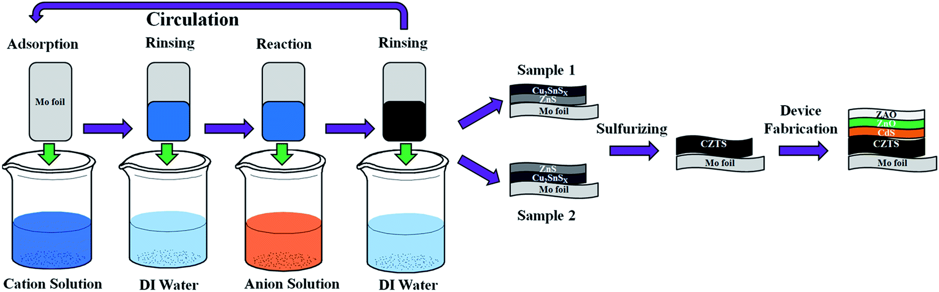 | ||
| Fig. 1 Schematic illustration for the fabrication of flexible CZTS solar cells on Mo foil. | ||
CdS buffer layers (60–80 nm) were deposited by conventional chemical bath deposition (CBD) method from aqueous solution of CdSO4 (0.003 M), thiourea (0.3 M) and ammonia (0.28 M) at 80 °C for 8 min. ZnO window (80 nm) and ZnO:Al (AZO) (400 nm) layers were subsequently deposited by RF magnetron sputtering with a device area of approximately 0.15 cm2.
The chemical composition, surface morphology, thickness and crystalline properties of CZTS absorber layers were characterized by energy dispersive X-ray spectroscopy (EDS, EDAX-GENSIS60S), scanning electron microscopy (SEM, FEI Quanta-200), Step profiler (Dektak 150) and X-ray diffraction (XRD Rigaku3014) respectively. The Raman spectra were taken by using a Jobin-YvonLabRam HR800-Horiba spectrometer (with 532 nm excitation wavelength). The optical properties of CZTS absorber layers were determined by Shimadzu UV-3600 spectrophotometer. Current–voltage (J–V) measurements were performed under simulated AM 1.5 Global spectrum and 100 mW cm−2 (1 sun) illumination with a Keithley 2400 source meter and a solar simulator.
3. Results and discussion
The chemical compositions of both absorber layers on Mo foil substrates are Cu poor and Zn rich before and after sulfurizing as shown in Table 1, which are in the desired composition range of those reported high efficiency CZTS solar cells.4,9,26 The ratios of Zn/Sn for both samples increased after sulfurizing mainly due to the volatilization of Sn during the sulfurization process, which also contributed to the slight increase of Cu/(Sn + Zn). In addition, the S contents are slightly increased after sulfurizing owing to the relatively high sulfur pressure during sulfurization process, which can be helpful to improve the efficiency of CZTS solar cells.26,27 Thickness of the absorber layers was characterized with reference samples on glass substrates because of the high roughness of the Mo foil. It can be seen that the thickness of the absorber layers did not change significantly during sulfurizing process, suggesting a slight volume expansion because the precursors contain sufficient sulfur.| Sample | Ratio | Thickness (nm) | |||
|---|---|---|---|---|---|
| Cu/(Sn + Zn) | Zn/Sn | S/Metal | |||
| 1 | Precursor | 0.74 | 1.13 | 0.97 | 660 |
| Sulfurized | 0.76 | 1.28 | 1.11 | 710 | |
| 2 | Precursor | 0.75 | 1.15 | 0.95 | 670 |
| Sulfurized | 0.78 | 1.25 | 1.07 | 700 | |
Fig. 2 demonstrates X-ray diffraction (XRD) data of the absorber. Due to less than 1 μm thickness of the absorber layers, clear diffraction peaks of the Mo substrate and MoS2 can be detected. Besides the Mo and MoS2 peaks, both samples demonstrate highly crystalline single phase Cu2ZnSnS4 (JCPDS 26-0575: standard unit cell volume of 319.5 Å). All peaks of the two samples correspond well with the tetragonal CZTS (JCPDS 26-0575) without any impurity phase within sensitivity limit of the instrument. Nevertheless, owing to the strong influence of the Mo substrate, it is difficult to make a conclusion which sample has a better crystallinity, although the intensity of diffraction peaks of Sample 2 are a little higher than that of Sample 1.
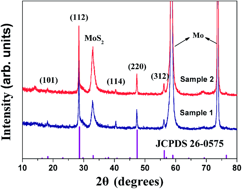 | ||
| Fig. 2 XRD patterns for two sulfurized absorber layers and the standard XRD pattern for CZTS (vertical bars: standard JCPDS 26-0575). | ||
It is universally accepted that XRD alone is insufficient to determine the phase purity of CZTS, since Cu2SnS3 and ZnS share similar crystal structure which lead to the similar diffraction patterns within the instrument accuracy. Therefore, the structural properties were further investigated by Raman spectroscopy to probe the surface of the films due to its complimentary capability to distinguish binary or ternary phase and its lower impurity detection limits than XRD. Fig. 3 shows the Raman spectra of absorber layers from different stacked structure precursor films. Peaks corresponding to the CZTS compound were observed at 286, 337, and 368 cm−1, in excellent agreement with literature. However, Raman spectra show the presence of SnS with characteristic mode at 160 cm−1, corresponding with data reported by other authors.28,29 Furthermore, the principal peak of the Sample 2 at 337 cm−1 is broader and has a relatively low intensity compared with that of Sample 1. This is more accurate than XRD due to its superficial detection depth which can hardly be influenced by the Mo foil substrate. The result indicates that the crystal quality of CTS/ZnS/Mo precursor based CZTS absorber layers is better than that of ZnS/CTS/Mo based absorber layers.
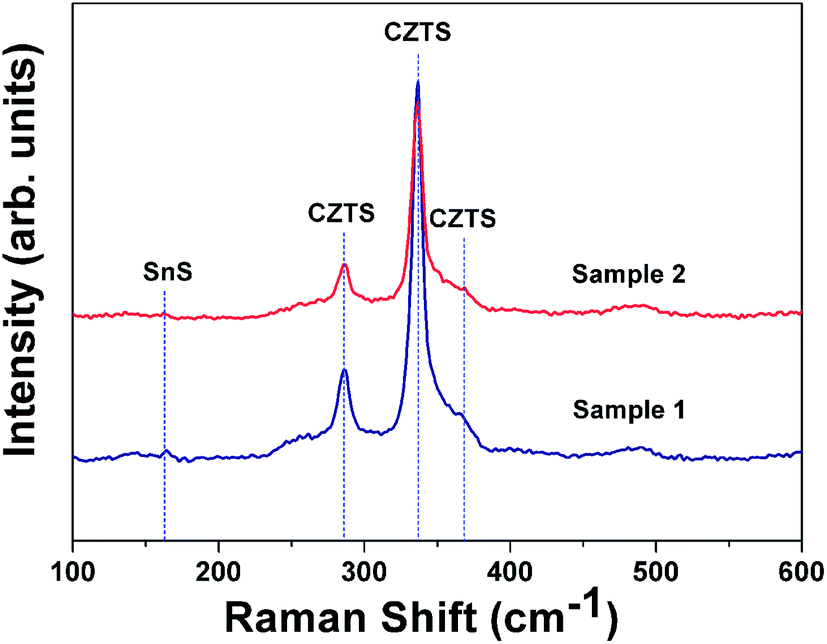 | ||
| Fig. 3 Raman spectra for two sulfurized absorber layers (with same intensity scale). | ||
Fig. 4 illustrates the surface scanning electron microscopy (SEM) images of the precursor and sulfurized films for both absorber layers. The left (a and c) are precursor films and the right (b and d) are sulfurized films. Both precursor films show amorphous morphology because of the low deposition temperature. In addition, due to the high roughness of the Mo foil substrate and less than 1 μm thickness of the absorber layers, the surface of the precursor films demonstrate gullies in accordance with the substrates. After sulfurizing, the surface of the sulfurized films appears granular and homogeneous with the agglomerated particles well distributed through the whole surface. The demonstrated compact and uniform microstructure benefited from the growth mechanism of SILAR method, which is necessary for high conversion efficiency of thin film solar cells. Moreover, it is known that different stack sequence in precursors can significantly affect the surface morphology of films.30–32 It is reasonable to expect the difference in SEM images for two sulfurized films. Comparing the morphology of two sulfurized films, the grain sizes of Sample 1 are larger than that of Sample 2, which lead to more grain boundaries in Sample 2 than Sample 1. As is well-known that large grain size and less grain boundary are beneficial to improve the device efficiency, Sample 1 may have a better performance than Sample 2 because smaller grains with excess grain boundaries may lead to recombination which generates loss in Voc and cause a reduction in current without sufficient passivation. However, there are a little voids or cracks on the surface of both samples, which may hinder the performance of device.
 | ||
| Fig. 4 Surface morphologies for absorber layers Sample 1 (a and b) and Sample 2 (c and d) before and after sulfurizing. | ||
Samples deposited on SLG substrates with the same procedure on Mo foil substrates were used to characterize the optical absorptions of the absorber layers. Fig. 5 depicts the absorption spectra of both CZTS thin films in the wavelength of 400–2000 nm, where α and hv are the absorption coefficient and the photo energy, respectively. It shows that both samples have remarkably high absorption coefficient of 104 cm−1 especially in the visible wavelength. It is notable that the absorption coefficient of Sample 1 is twice as that of Sample 2 probably resulted from the difference of the crystallinity. What's more, as shown in the inset, the value of Eg obtained by extrapolating the linear region of the plot of the absorption squared versus energy are 1.50 and 1.41 eV for Sample 1 and Sample 2 respectively, agreeing well with the earlier reported values.
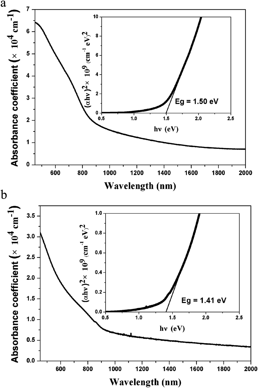 | ||
| Fig. 5 The optical absorption spectra and estimations of band gap energy for absorber layers Sample 1 (a) and Sample 2 (b) on SLG. | ||
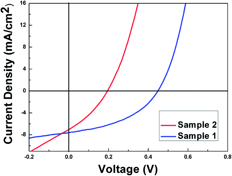
The current density–voltage (J–V) curves of solar cells with different stacked structure based absorber layers are presented in Fig. 6. Sample 1 with the stacked order of CTS/ZnS/Mo yields an efficiency of 2.42% with an open circuit voltage Voc = 477 mV, a short circuit density Jsc = 11.29 mA cm−2, and a fill factor FF = 45%, which is the highest flexible cell achieved so far in our lab. In contrast, Sample 2 with the stacked order of ZnS/CTS/Mo demonstrates only 0.61% efficiency (Voc = 196 mV, Jsc = 9.55 mA cm−2 and FF = 33%) probably due to the above facts of poorer crystallinity, smaller grain size and more grain boundaries without good passivation. These problems could result in a severe bulk recombination and higher series resistance, which will limit the Voc and FF, thereby hinder the efficiency of the device.
 | ||
| Fig. 6 J–V characteristic of CZTS solar cells based on different stacked structure precursors. | ||
To gain further insights in the device performance, the cross-sectional SEM image of Sample 1 was obtained by characterizing the cell fragments which were processed by quenching in liquid nitrogen because of the toughness of Mo foil. As shown in Fig. 7(a), the absorber quality is greatly inferior to those reported columnar grains on rigid substrates,4,5 which demonstrates a large number of smaller grains. The formation of smaller grains shown in Fig. 7(a) is mainly because of the higher surface roughness of the Mo foil substrate than that of Mo coated SLG, since rougher surface could introduce a large number of nucleation center. The nucleation center will in return reduce the grain size and increase the grain boundaries, which not only results in severe recombination at the grain boundaries if without sufficient passivation but also leads to significant blocking of the carrier transportation and thereby higher series resistance. This might explain the obvious losses in open circuit voltage and current density. Another factor that limits the efficiency indicated from the image is the thick window layer. Over 1 μm AZO layer would reduce the incident short wavelength visible light that can be absorbed by the absorber, which will lower the quantum efficiency and then decrease the Jsc. The Jsc losses can also be confirmed by the external quantum efficiency (EQE), as showed in Fig. 7(b), which demonstrates the maximum around 60% quantum efficiency. By the way, it should be mentioned that the band gap calculated from the EQE spectrum is 1.38 eV (Fig. 7(b) inset), which is a bit smaller than the data calculated from the optical absorption spectra on SLG substrate. This might be explained by the defect level in the films. The third problem to note is the role of secondary phase. In particular, the SnS detected from Raman spectra will limit the open circuit voltage of the solar cell due to its lower band gap than the CZTS absorber.33 It is even worse if SnS precipitated along the grain boundaries because the CZTS/SnS interface is a strong sink for carriers and the recombination velocity for the interface is high, which is mainly attributed to the difference in crystal structure between CZTS and SnS.34 Finally, the observation of the pronounced cross-over behavior between the light and dark J–V curves of Sample 1, as shown in Fig. 7(c) reveals a high back-contact barrier in CZTS,35,36 which suppresses the major carrier transport and contributes to a large series resistance and low Jsc and FF. Indeed, the series resistance Rs of Sample 1 is 9 Ω cm2, much higher than those of high performance devices.4,5 In short, this research is at an early stage and may be associated with processing variables, but these results could lead to a promising fabrication route for achieving efficient flexible devices.
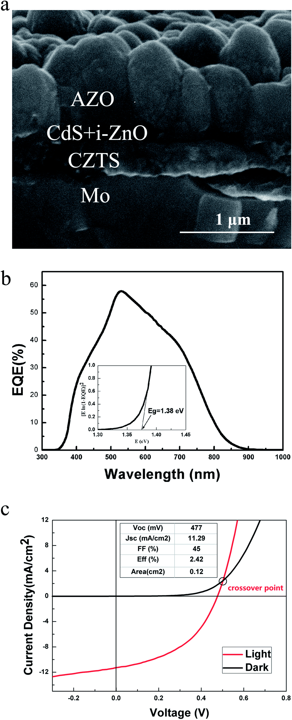 | ||
| Fig. 7 Cross section SEM image (a), external quantum efficiency spectrum (inset: band gap calculated from the EQE spectrum) (b) and light and dark J–V curve (c) of the best device. | ||
4. Conclusion
Flexible Cu2ZnSnS4 solar cells based on sulfurizing stacked precursor films deposited by SILAR method on Mo foil substrates have been fabricated, and demonstrate the efficiency of 2.42%. Comparative studies of different stacked precursors reveal that device from Cu2SnSx/ZnS/Mo (Sample 1) precursor has a better performance due to better crystallinity, morphology and electric properties of the absorber layer. Although yielding a preferable efficiency, the best device performance is still significantly lower compared with others' reported CZTS cells on rigid SLG substrates. This is mainly because the device still suffers from a large number of grain boundaries, thick AZO layer and detrimental secondary phases. Addressing the device shortcomings noted above is expected to enable our flexible CZTS device to achieve a future performance gains.Acknowledgements
This work was supported by the National High Technology Research and Development Program of China (863 Program, no. 2011aa050528), the National Natural Science Foundation of China (no. 51204214) and Fundamental Research Funds for the Central Universities of Central South University (no. 2013zzts192). Authors from University of New South Wales acknowledge the sponsorship by the Australian Government through the Australian Research Council (ARC) and the Australian Renewable Energy Agency (ARENA). The Australian Government, through ARENA, is supporting Australian research and development in solar photovoltaic and solar thermal technologies to help solar power become cost competitive with other energy sources.References
- M. Powalla and B. Dimmler, Thin Solid Films, 2001, 387, 251–256 CrossRef CAS.
- M. A. Green, K. Emery, Y. Hishikawa, W. Warta and E. D. Dunlop, Prog. Photovoltaics, 2014, 22, 1–9 Search PubMed.
- A. Chirila, P. Reinhard, F. Pianezzi, P. Bloesch, A. R. Uhl, C. Fella, L. Kranz, D. Keller, C. Gretener, H. Hagendorfer, D. Jaeger, R. Erni, S. Nishiwaki, S. Buecheler and A. N. Tiwari, Nat. Mater., 2013, 12, 1107–1111 CrossRef CAS PubMed.
- B. Shin, O. Gunawan, Y. Zhu, N. A. Bojarczuk, S. J. Chey and S. Guha, Prog. Photovoltaics, 2013, 21, 72–76 CAS.
- T. K. Todorov, J. Tang, S. Bag, O. Gunawan, T. Gokmen, Y. Zhu and D. B. Mitzi, Adv. Energy Mater., 2013, 3, 34–38 CrossRef CAS.
- Z. Zhou, Y. Wang, D. Xu and Y. Zhang, Sol. Energy Mater. Sol. Cells, 2010, 94, 2042–2045 CrossRef CAS PubMed.
- Q. Tian, X. Xu, L. Han, M. Tang, R. Zou, Z. Chen, M. Yu, J. Yang and J. Hu, CrystEngComm, 2012, 14, 3847–3850 RSC.
- H. Katagiri, K. Jimbo, S. Yamada, T. Kamimura, W. S. Maw, T. Fukano, T. Ito and T. Motohiro, Appl. Phys. Express, 2008, 1, 041201 CrossRef.
- V. Chawla and B. Clemens, in Photovoltaic Specialists Conference (PVSC), 2012 38th IEEE, 2012, pp. 002990–002992 Search PubMed.
- Y. B. Kishore Kumar, G. Suresh Babu, P. Uday Bhaskar and V. Sundara Raja, Sol. Energy Mater. Sol. Cells, 2009, 93, 1230–1237 CrossRef CAS PubMed.
- Q. Guo, G. M. Ford, W.-C. Yang, B. C. Walker, E. A. Stach, H. W. Hillhouse and R. Agrawal, J. Am. Chem. Soc., 2010, 132, 17384–17386 CrossRef CAS PubMed.
- Y. Cao, M. S. Denny, J. V. Caspar, W. E. Farneth, Q. Guo, A. S. Ionkin, L. K. Johnson, M. Lu, I. Malajovich, D. Radu, H. D. Rosenfeld, K. R. Choudhury and W. Wu, J. Am. Chem. Soc., 2012, 134, 15644–15647 CrossRef CAS PubMed.
- K. Tanaka, Y. Fukui, N. Moritake and H. Uchiki, Sol. Energy Mater. Sol. Cells, 2011, 95, 838–842 CrossRef CAS PubMed.
- W. Ki and H. W. Hillhouse, Adv. Energy Mater., 2011, 1, 732–735 CrossRef CAS.
- S. Ahmed, K. B. Reuter, O. Gunawan, L. Guo, L. T. Romankiw and H. Deligianni, Adv. Energy Mater., 2012, 2, 253–259 CrossRef CAS.
- L. Guo, Y. Zhu, O. Gunawan, T. Gokmen, V. R. Deline, S. Ahmed, L. T. Romankiw and H. Deligianni, Prog. Photovoltaics, 2013, 22, 58–68 Search PubMed.
- Y. F. Nicolau, Appl. Surf. Sci., 1985, 22–23(2), 1061–1074 CrossRef CAS.
- J. Yang, Z. Jin, T. Liu, C. Li and Y. Shi, Sol. Energy Mater. Sol. Cells, 2008, 92, 621–627 CrossRef CAS PubMed.
- Y. Shi, Z. Jin, C. Li, H. An and J. Qiu, Appl. Surf. Sci., 2006, 252, 3737–3743 CrossRef CAS PubMed.
- J. J. Li, Y. A. Wang, W. Guo, J. C. Keay, T. D. Mishima, M. B. Johnson and X. Peng, J. Am. Chem. Soc., 2003, 125, 12567–12575 CrossRef CAS PubMed.
- H. Lee, M. Wang, P. Chen, D. R. Gamelin, S. M. Zakeeruddin, M. Grätzel and M. K. Nazeeruddin, Nano Lett., 2009, 9, 4221–4227 CrossRef CAS PubMed.
- S. S. Mali, P. S. Shinde, C. A. Betty, P. N. Bhosale, Y. W. Oh and P. S. Patil, J. Phys. Chem. Solids, 2012, 73, 735–740 CrossRef CAS PubMed.
- N. M. Shinde, D. P. Dubal, D. S. Dhawale, C. D. Lokhande, J. H. Kim and J. H. Moon, Mater. Res. Bull., 2012, 47, 302–307 CrossRef CAS PubMed.
- S. S. Mali, B. M. Patil, C. A. Betty, P. N. Bhosale, Y. W. Oh, S. R. Jadkar, R. S. Devan, Y.-R. Ma and P. S. Patil, Electrochim. Acta, 2012, 66, 216–221 CrossRef CAS PubMed.
- Z. Su, C. Yan, K. Sun, Z. Han, F. Liu, J. Liu, Y. Lai, J. Li and Y. Liu, Appl. Surf. Sci., 2012, 258, 7678–7682 CrossRef CAS PubMed.
- K. Jimbo, R. Kimura, T. Kamimura, S. Yamada, W. S. Maw, H. Araki, K. Oishi and H. Katagiri, Thin Solid Films, 2007, 515, 5997–5999 CrossRef CAS PubMed.
- H. Katagiri, Thin Solid Films, 2005, 480–481, 426–432 CrossRef CAS PubMed.
- P. A. Fernandes, P. M. P. Salomé and A. F. da Cunha, Thin Solid Films, 2009, 517, 2519–2523 CrossRef CAS PubMed.
- P. A. Fernandes, P. M. P. Salomé and A. F. da Cunha, J. Alloys Compd., 2011, 509, 7600–7606 CrossRef CAS PubMed.
- H. Yoo and J. Kim, Sol. Energy Mater. Sol. Cells, 2011, 95, 239–244 CrossRef CAS PubMed.
- H. Yoo and J. Kim, Thin Solid Films, 2010, 518, 6567–6572 CrossRef CAS PubMed.
- S. W. Shin, S. M. Pawar, C. Y. Park, J. H. Yun, J.-H. Moon, J. H. Kim and J. Y. Lee, Sol. Energy Mater. Sol. Cells, 2011, 95, 3202–3206 CrossRef CAS PubMed.
- S. Siebentritt, Thin Solid Films, 2013, 535, 1–4 CrossRef CAS PubMed.
- B. G. Mendis, M. C. J. Goodman, J. D. Major, A. A. Taylor, K. Durose and D. P. Halliday, J. Appl. Phys., 2012, 112, 124508 CrossRef PubMed.
- O. Gunawan, T. K. Todorov and D. B. Mitzi, Appl. Phys. Lett., 2010, 97, 233506 CrossRef PubMed.
- K. Wang, O. Gunawan, T. Todorov, B. Shin, S. Chey, N. Bojarczuk, D. Mitzi and S. Guha, Appl. Phys. Lett., 2010, 97, 143508 CrossRef PubMed.
| This journal is © The Royal Society of Chemistry 2014 |