DOI:
10.1039/C3RA47689H
(Paper)
RSC Adv., 2014,
4, 8064-8071
Direct conjugation of DNA to quantum dots for scalable assembly of photoactive thin films†
Received
16th December 2013
, Accepted 7th January 2014
First published on 14th January 2014
Abstract
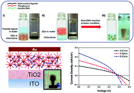
For many thin film applications, it is critical to not only control the organization of the materials on surfaces but to also use scalable processes that are time and material efficient. This is especially the case when using nanomaterials, including metal or semiconductor nanocrystals, as building blocks from which to engineer devices. In this work, we demonstrate a method to directly conjugate DNA to cadmium based quantum dots (QD) to create thin film arrays on surfaces for potential optoelectronic devices. These DNA-conjugated QDs showed uniform coatings, were oxidation-stable, and remained stable in high ionic strength environments. In previously published work, we discovered that high salt, in particular magnesium, is critical for fabricating nanoparticle assemblies on substrates through DNA interactions. The QD thin films were produced by means of interparticle DNA hybridization in a few steps with no loss of material and with good control over film thickness and roughness. By directly conjugating the DNA to the QDs, it also became possible to study DNA's role in mediating charge transport in the QD films. For this, DNA-conjugated CdTe nanocrystals were assembled onto TiO2 films to fabricate photovoltaic prototypes. Current–Voltage measurements from the DNA–QD devices showed the promise of using DNA not only as an assembler but also as mediator of charge separation and transport.
Introduction
Semiconductor nanocrystals such as quantum dots (QDs) have been heavily investigated in recent years as potential building blocks for optoelectronic devices.1–9 The tunable size-dependent bandgap of QDs has afforded methods to optimize device performance and enhance photon absorption. In addition, the solution processability of nanomaterials allows fabrication techniques that are less expensive and time-consuming than techniques such as vacuum deposition. Despite some of these key advantages, however, utilizing QDs for optoelectronics has remained a challenge due to the inherent surface defects of nanocrystals10 and difficulties in producing close-packed films with minimal roughness and smooth interfaces in only one or two steps and with limited waste of material.11–17 Methods such as slow evaporation or liquid-air interfacial assembly provide limited control over film thickness and roughness while spin-coating requires multiple steps, each of which can waste large amounts of nanocrystals and solvents. Furthermore, the common ligands used for synthesizing semiconductor nanocrystals are typically hydrocarbon based and therefore insulating, leading to deleterious effects on carrier mobility in devices. One possibility to address some of these challenges in nanofabrication would be to use a molecular ligand that not only can promote particle assembly on surfaces but might also permit electron transport for device applications. One particular chemical that may address this is DNA where DNA hybridization has been used to promote assembly of nanomaterials in solution and on surfaces18–28 and has also been shown to mediate charge transport. In recent years, many groups have performed nanosecond transient absorption measurements and electrical measurements to determine the efficiency and kinetics of electron and hole transport in DNA tracts.29–35 In addition, other reports have shown that electronic charge transport can be facilitated through DNA π–π stacking36–39 as well as through 34 nm long dsDNA in electrochemical measurements.40
In order to use DNA for assembling semiconductor nanocrystals into photoactive thin film arrays, we demonstrate here methods to conjugate DNA directly to QDs so as to avoid the use of highly insulating lipid bilayers or polymer coatings typically used for QD bioconjugation.41–44 In addition, these methods produced DNA–QDs that were highly stable to oxidation and remained well dispersed in divalent salts up to 125 mM MgCl2. The stability in magnesium was critical to achieve since we previously found that magnesium is necessary to obtain nanoparticle binding to DNA templates45 or enable nanoparticle close-packing on surfaces through interparticle DNA hybridization.46 These DNA conjugated QDs were then used to produce QD thin films in a few steps with controllable film thicknesses and with no material waste. Finally, because the DNA strands were directly conjugated to the QDs, we could study the effect of DNA on charge separation for optoelectronic devices. For this, test ITO/TiO2/DNA–CdTe/Au thin film devices were fabricated that showed observable photovoltaic effects, supporting the idea that DNA incorporation in QD thin films does not completely impede charge transport.
Materials and methods
Quantum dot synthesis
CdTe and CdSe quantum dots were prepared with minor modifications following the method reported by Chen et al.47 CdS quantum dots were prepared with minor modifications following the method reported by Peng et al.48
Synthesis of CdTe quantum dots. The TOP–Te solution was prepared dissolving 0.035 g tellurium (Alfa Aesar, 99.99%) in 0.313 g trioctylphosphine (TOP) (Sigma-Aldrich, 90%) under nitrogen at 250 °C for 3 h until the solution turned light yellow. The CdO solution was prepared by mixing 0.035 g cadmium oxide (CdO) (Alfa Aesar, 99.998%), 0.275 g octadecylphosphonic acid (Sigma-Aldrich, 97%) and 3.725 g trioctylphosphine oxide (TOPO) (Sigma Aldrich, 99%) in a 100 mL flask at 100 °C for 3 h under nitrogen. The CdO solution was then heated to 325 °C and injected with the TOP–Te solution shortly thereafter. The reaction was then cooled to 315 °C followed by a growth step. Running the growth reaction for 1.5 minutes, 6 minutes and 8 minutes yielded ∼4.81 nm, 5.69 nm and 6.53 nm CdTe QDs, respectively. The size was determined both by absorbance49 and TEM images. Toluene was added to a batch of CdTe QDs when cooled to 60 °C followed by bulk centrifugation to remove unreacted raw materials. To remove excess organics, the CdTe QDs were precipitated out using methanol followed by bulk centrifugation with 3 times repeat.
Synthesis of CdSe quantum dots. The TOP–Se solution was prepared using 0.039 g selenium (Alfa Aesar, 99.5%) and 500 mg TOP (Sigma-Aldrich, 90%). Se was dissolved in TOP and mixed until the solution became transparent. The CdO solution was prepared by mixing 0.0256 g CdO, 0.227 g stearic acid (sigma Aldrich, 98.5%) and 8 mL 1-octadecene (ODE) (Sigma Aldrich, 90%) in a 100 mL flask. After the CdO was dissolved at 210 °C, the solution was cooled down to room temperature and 1 g octadecylamine (Sigma Aldrich) and 1 g TOPO were added. The solution was degassed for 3 h at 100 °C followed by heating to 300 °C and injection with the TOP–Se solution. After injection the reaction was cooled down to 280 °C and further reacted for 30 min to generate ∼4.2 nm CdSe nanoparticles. To wash the CdSe nanoparticles, toluene was added to the CdSe QD solution held at 60 °C, being followed by bulk centrifugation to remove unreacted raw materials. To remove excess organics, the CdSe QDs in toluene were precipitated out using acetone and methanol successively.
Synthesis of CdS quantum dots. The S solution was prepared dissolving 0.0064 g sulfur (Sigma Aldrich, 99.5%) in 2 mL ODE. The CdO solution was prepared by mixing 0.025 g CdO, 0.165 g oleic acid (Sigma Aldrich, 90%) and 10 mL ODE in a 100 mL flask. The temperature was elevated to 90 °C and the flask was placed under vacuum for 1 h. The flask was then re-filled with nitrogen and the reaction mixture was heated to 210 °C and stirred until the solution became optically transparent. The CdO solution was then heated to 250 °C and injected with the S solution shortly thereafter. The growth reaction was then run for 45 min, resulting in ∼5.7 nm CdS QDs. Toluene was added to a batch of CdS QDs when cooled to 60 °C, being followed by bulk centrifugation to remove unreacted raw materials. To remove excess organics, the CdS QDs in toluene were precipitated out using acetone and methanol successively.
DNA conjugation to CdX (X = Se, Te, S) QDs
The CdX QDs were dissolved in chloroform. A thioglycerol (Sigma Aldrich, 99%) solutions were prepared in 5 mM phosphate buffer for CdTe QDs and 0.1 M NaOH solution for CdSe and CdS QDs, respectively. It was then added to the CdX QDs in chloroform using CdX
:
thioglycerol molar ratios of 1
:
105 (0.25 M thioglycerol for 5.7 nm CdX). Biphasic solutions formed and were mixed vigorously (>15 min.) until the CdX QDs were completely transferred to the aqueous phase. The water soluble CdX QDs were then collected and the excess thioglycerol was removed by using a 30 K centrifuge filter (Pall Corporation). At the same time, thiolated DNA was prepared by first reducing the commercially purchased DNA (Integrated DNA Technologies) with tris(2-carboxyethyl)phosphine hydrochloride (TCEP–HCl) (Thermo Scientific) for 1 h followed by removing excess TCEP by dialysis (1 K MWCO, GE Healthcare). The reduced DNA was immediately added to the thioglycerol conjugated CdX QDs with 0.1 M NaOH using CdX
:
DNA ratios of 1
:
200 for a size of 4.2 nm CdX QDs. After overnight reaction, excess DNA was removed by using a 30 K centrifuge filter and the final DNA–CdX solution was stored in 5 mM phosphate buffer.
Device fabrication
TiO2 film deposition. TiO2 nanoparticles (Ti-Nanoxide HT/SC) were purchased from Solaronix Inc. The TiO2 films were prepared on ITO glass (Delta Technologies, 10 Ω cm−2) by spin coating at 3000 rpm for 15 s. One end of the TiO2 film was wiped with ethanol for ITO contact during current–voltage measurements followed by annealing at 450 °C for 10 min. The TiO2 films were additionally treated with 50 mM TiCl4 (Sigma Aldrich) at 70 °C for 30 min and followed by a second annealing at 450 °C for 10 min.50
QD film deposition. Two sets of DNA conjugated QDs one bound with 5′SH-T10 (polythymine) and the other with 3′SH-T10 were mixed together in 10 mM MgCl2 with linker DNA An (polyadenine, n = 10–15) which is used to promote interparticle hybridization. First, the area of the TiO2 substrate where the DNA–QD film were to be deposited was defined by UV exposure with O2 atmosphere by using a shadow mask. The DNA–QD solutions were then dropped onto the TiO2 substrates and adsorbed for 1 h under humid conditions followed by vacuum treatment for a few minutes to remove excess solvent. The films were then washed briefly with 90/10 (v/v %) ethanol/water to remove excess salts. Next, the DNA–QDs were thermally annealed under humid conditions at 60 °C for 1 h to promote ordering and cooled down slowly (0.5°C min−1). The films were further heated under vacuum at 80 °C for 40 min to remove any remaining water molecules. Gold metal (Kurt J. Lesker, 99.999%) was next deposited on the DNA–QD film by thermal evaporation at a rate of 0.4 Å s−1 and 1.5 Å s−1 with 30 nm and 70 nm, respectively followed by a vacuum anneal for 40 min at 80 °C to promote better metal contact.
Current–Voltage measurements
Current–Voltage measurements were performed using a Keithley 2400 source meter. The solar spectrum at AM1.5 was simulated to within class BBA specifications with a filtered tungsten lamp (PV Measurements). The source intensity (100 mW cm−2) was measured with a calibrated reference solar cell having an 8 mm diameter aperture from PV Measurements. The active area of the devices ranges from 1 mm2 to 1.5 mm2, as defined by the overlap of ITO and Au.
Instrumentations
UV-Visible spectrophotometry (UV-Vis). The UV-Vis absorbance was measured by Beckman Coulter DU 730 Life Science UV-Vis spectrophotometer, wavelength used for measurements was ranged between 200 and 900 nm.
Scanning electron microscopy (SEM). SEM images were taken by JEOL JSM 7401F, where acceleration voltage was 5 kV with a secondary electron mode.
Results and discussion
The strategy used for producing stable DNA conjugated CdX (X= S, Se, Te) quantum dots is depicted in Fig. 1a. First, a buffered thioglycerol (TG) solution was directly added to the as-synthesized CdX QDs in chloroform to form a biphasic mixture. Once the TG conjugated QDs were completely transferred to the aqueous phase, thiolated DNA was added at basic pH (>pKa) to facilitate binding between thiolate (S−) groups and the Cd surface.51 By using an intermediate ligand exchange method, we were able to easily conjugate high yields of DNA to each QD as well as impart stability to the DNA–QDs in buffer and high salt. The use of ligand exchange by replacing the long hydrocarbon ligands first with short molecules prior to addition of DNA led to a higher exchange yield with less steric hindrance for DNA binding to a QD surface. After each TG and DNA conjugation, the CdX QD solutions were run through microcentrifuge filters several times to remove excess ligands and the DNA–CdX QDs were finally stored in 5 mM phosphate buffer. (Fig. 1b)
 |
| Fig. 1 (a) Schematic of DNA–QD conjugation: (i) biphasic mixture consisting of QD in chloroform and thioglycerol in buffer solution (ii) phase transferred QD–thioglycerol solution followed after filtering out excess thioglycerol (iii) addition/reaction of HS-DNA to filtered QD–thioglycerol pellet followed by removal of excess DNA. (b) TEM images of DNA–QD (from left: CdSe, CdTe and CdS) and inset images are photos of DNA–QD solution after conjugation. Scale bar corresponds to 20 nm. | |
The optical properties of the DNA–CdX QDs and the uniformity of DNA coverage on the particles were next investigated by UV-Vis adsorption and gel electrophoresis. (Fig. 2 and S1†) In order to determine the stability of the DNA conjugated QDs against oxidation, the excitonic peaks of the DNA–QDs as dispersed in buffer were measured and in all cases, little to no blue shift in adsorption peaks was observed. However, it must be noted that in contrast to CdS and CdSe, there was a very small blue shift in the DNA–CdTe excitonic peak which corresponded to less than 0.22 nm decrease (0.18 nm for 4.81 nm, 0.17 nm for 5.69 nm and 0.22 nm for 6.53 nm, respectively) in CdTe dimension (Fig. 2a and S1†) and therefore smaller than the diameters of the individual Cd (0.3 nm) and Te (0.28 nm) atoms. These minor blue shifts in the CdTe absorbance were mainly observed during the thioglycerol ligand exchange in which unpassivated Te atoms on the QD surface is thought to readily react with oxygen, resulting in the formation of singlet oxygen molecules at the CdTe surface.52 In terms of the uniformity of the DNA coating on the CdX QDs, agarose gel electrophoresis showed sharp bands of the DNA–CdX QDs indicating that all the nanocrystals have roughly the same coverage of DNA (Fig. 2b). In addition, absorbance measurements of the DNA solutions before and after conjugation to the QDs showed that about 20 strands of DNA could be attached per nanocrystal (ESI†) Finally, after adding 125 mM MgCl2 to the DNA conjugated CdX QD solutions, the nanoparticles were found to be remarkably stable without forming any aggregates for at least 48 h while thioglycerol only coated CdX QDs left pellets on the bottom of the tubes right after MgCl2 addition (Fig. 2c). UV-Vis absorbance measurements of the DNA–QDs were run to characterize their stability in MgCl2 and as shown in Fig. S2,† increasing magnesium concentrations to 125 mM MgCl2 caused no blue or red shift in the QD excitonic peaks. It is believed that the highly negatively charged DNA acts as a buffer layer which keeps the Mg2+ ions away from the QD surface as well as provides enough electrostatic repulsion force between particles to prevent aggregation. Since magnesium was previously found to be essential for DNA-mediated NP assembly,28 this method of creating DNA–CdX QDs with stability to high salt and oxidation was critical for creating close packed thin films of QDs for optoelectronic applications. While other strategies have been used to attach DNA to QDs,53,54 the previous work to date has focused predominantly on attaching DNA to core–shell QDs-which cannot be applied then for optoelectronic devices and stability tests in high salt conditions or resistance to oxidation were also not studied. Furthermore, we found that when thioglycerol was replaced with the more commonly used acid terminated thiol groups such as thioglycolic acid that low DNA–QD yields were obtained and that oxidation was not prevented (Fig. S3†). When switching from thiols to amine terminated ligands, we found as had previously been reported55 that the weak binding between Cd and amine moieties were not favorable to prevent oxidation, resulting in dissolution of the QDs.
 |
| Fig. 2 (a) UV-Vis absorbance of as-synthesized CdTe QD solutions and DNA–QD solutions. (b) Agarose gel electrophoresis of DNA–QD solutions. (1.5%, left lane: 3′DNA–QDs and right lane: 5′DNA–QDs) (c) Photographs of DNA–QDs and Thioglycerol–QDs with 125 mM MgCl2 after 48 h (left two samples correspond to 5′DNA–QD and 3′DNA–QDs solutions, respectively and a sample in right is thioglycerol only coated QDs solution). | |
Next, we decided to produce close packed nanoparticle thin films by using the DNA–QDs and by promoting interparticle DNA hybridization by use of DNA “linkers”.28 Because we also wanted to explore the effect of DNA on charge transport through the QD films, we focused on using the p-type DNA conjugated CdTe QDs to build p–n heterojunction based solar cells that consist of ITO/TiO2/DNA–CdTe/Au. Based on the energy levels, the CdTe QDs would act as a hole transport absorbing layer and is also energetically well matched to TiO2. CdSe and CdS on the other hand are n-type semiconductors like TiO2 and also have CB levels that do not match favorably with that of TiO2. TiO2 films were first deposited on ITO by spin-coating commercial TiO2 nanoparticle solutions (Solaronix Inc.) at 3000 rpm for 15 s, sintering at 450 °C for 10 min followed by treatment with 50 mM TiCl4 at 70 °C for 30 min and a final sintering step. Next, equimolar solutions of 5′SH-T10–CdTe, 3′SH-T10–CdTe in 10 mM MgCl2 were mixed with polyadenine (An, n = 10–15) DNA (“linker DNA”) at 0.5–1 molar ratios of linker DNA to DNA on CdTe which promotes interparticle hybridization between the 5′ and 3′ DNA–QDs. Next, the solutions were adsorbed to the sintered TiO2 surfaces followed by drying in vacuum for 5 minutes and rinsing with 90/10 (v/v %) ethanol/water to remove excess salts from the films while keeping the nanocrystals on the surface. By using polyadenine strands as DNA linkers with MgCl2 to promote interparticle hybridization and MgCl2, uniform QD films (Fig. 3a) could be produced. Without any DNA linkers added, after adsorbing and drying, the films produced clearly showed large deviations in film thickness between the edge and inner portion of the droplet (Fig. S4†). After adsorption and vacuum drying, the DNA–CdTe films underwent humid annealing at 60 °C to further promote DNA interactions followed by vacuum annealing at 80 °C for 40 min to remove water. Finally, a gold electrode was deposited on top of the DNA–CdTe layer (Fig. 3b). Because the entire method only required adsorbing the DNA–CdTe solutions followed by drying and thermal annealing, it was also very simple to produce films of variable thicknesses by tuning the initial DNA–CdTe concentrations (Fig. 3c and d). As shown in Fig. 3d, as we increased the QD concentrations from 1 uM to 5 uM, there was a clear gradation in color that corresponded to increases in film thicknesses. Cross-sectional SEM images (Fig. 3d and S5†) of the DNA–CdTe films on TiO2 showed not only a clear correlation between film thickness and QD concentration but that the films remained relatively smooth and that the QD–DNA layers were intact throughout the film.
 |
| Fig. 3 (a) Schematic of DNA(T10)–QD film fabrication on TiO2/ITO film with linker A10 DNA. (b) Layout of the ITO/TiO2/DNA(T10)–QD film/Au devices tested. (c) Plot showing the thickness of the DNA(T10)–QD films obtained as a function of the concentration of the DNA(T10)–QD solutions used. (d) Cross-sectional SEM images and optical images of films obtained using different concentrations (1 uM–5 uM) of 6.53 nm CdTe–DNA(T10) with A10 linker DNA. Scale bar corresponds to 200 nm. | |
For the photovoltaic studies, DNA–CdTe QD films composed of different sized nanocrystals (4.81 nm, 5.69 nm and 6.53 nm) was prepared and devices were tested first as a function of QD size and later film thickness. When comparing the effect of QD size, all of the DNA–CdTe layers within the ITO/TiO2/DNA–CdTe/Au devices were held constant at ∼140 nm. All of the devices from the different sized CdTe QDs showed consistent and reasonable current–voltage characteristics where the open circuit voltages (Voc) were set around 400 mV while the short circuit currents (Jsc) showed an increase with the larger QDs (Fig. 4a). One possible reason why Jsc would increase with CdTe size is simply that more light is absorbed with the increase in the CdTe QD size. Based on the reference solar spectra from National Renewable Energy Labs (NREL) (100 mW cm−2), linear correlations between absorbed input power (Pinput) and Jsc could be observed assuming the overall fill factors (FF) and Voc values remain similar enough (ESI†). In order to test the effect of film thickness on PV behavior, the 6.53 nm CdTe QDs were chosen since they showed the highest performance out of the three sizes of CdTe QDs. As shown in the summarized results of the current–voltage characteristics in Fig. 4b, while the device made from 1 uM DNA–CdTe solution was mostly shunted due to the films being too thin,56 as we increased in DNA–CdTe concentration from 2 uM to 5 uM, Jsc values decreased although Voc remained constant. As is typically observed with nanocrystal solar cells, having too thick a film is likely to hinder carrier transport due to increased recombination events. Among the devices tested, the use of 2 uM CdTe QD (film thickness = 140 nm) produced the photovoltaic effect with Jsc of 0.24 mA cm−2, Voc of 0.38 V, and FF of 0.34. Furthermore, the DNA–QD films were found to be stable against oxidation as no change the absorption onset peak was observed and current–voltage measurements after several weeks showed minimal decrease in Jsc and Voc was held constant (Fig. S6†). On the other hand, films made with no linker DNA showed absolutely little to no consistency in current–voltage characteristics as a function of QD size (Fig. S7†). It is hypothesized that the random formation of QD organization within the no DNA linker films resulted largely in irreproducible and poor device performances.
 |
| Fig. 4 (a) Current–Voltage curves for different sized DNA(T10)–CdTe QDs film. (b) Current–Voltage curves for different thicknesses of the DNA(T10)-6.53 nm CdTe QDs layer. | |
Effective separation of electron–hole pairs is critical to achieve a photovoltaic effect. In the case of nanocrystals, the electronic coupling between particles decreases exponentially as a function of interparticle distance.57 For example, when the ligands on the QDs are the hydrocarbons used for their synthesis, the coupling energy diminishes an order of magnitude every ∼2 Å increase in interparticle distance. In previous work with small area (3–5 micron) DNA–gold nanoparticle superlattices, we determined that the interparticle distance is primarily driven by the lengths of the dsDNA used.28 If this is roughly maintained with these large area (over 3 × 3 mm2) DNA–QD films, the spacing (surface to surface distance) between the CdTe nanocrystals is theoretically calculated to be ∼3 nm. Should this be the case, the distance between neighboring CdTe QDs is potentially too long to assume easy carrier hopping from one particle to the next which lends to the possibility that the DNA itself plays a role in enabling carrier migration. While electron mobility through double stranded DNA has been demonstrated,40,58–60 in the case of semiconductors, it is important to also consider effective charge separation at the DNA–QD interface, matching the relative LUMO–HOMO levels of the DNA attached to the nanoparticle with the conduction band(CB)–valence band(VB) of the QDs. In order to elucidate relative energy levels of DNA and QDs, single nanoparticle studies using DNA–QD constructs are currently being investigated through Scanning Tunneling Microscopy (STM) measurements.
Conclusion
In this work, a two-step method was demonstrated to conjugate DNA directly to the surface of cadmium chalcogenide QDs for optoelectronic applications. First, by using thioglycerol for intermediate ligand exchange, high yields of CdX (X = S, Se, Te) QDs could be transferred from organic solvents to water, followed by direct attachment of thiolated DNA. The DNA conjugated QDs remained stable in high ionic strength environments and to oxidation. These DNA–QDs were further assembled into close packed QD films in a few steps by using DNA–DNA interactions, with the thickness of the QD films easily tuned by simply changing the initial DNA–QD concentration. In solar cell test devices, current–voltage measurements showed that the DNA strands did not prevent electron–hole separation, and a photovoltaic effect was observed upon illumination. Future studies will investigate carrier mobility through these DNA–QD films as well as discrete nanoparticle structures to understand the influence of DNA on charge separation and energy transfer.
Acknowledgements
This work was supported by the Office of Naval Research (award number: N00014-09-01-0258), a DOE Early Career Award (DE-SC0006398), National Science Foundation (CMMI-0856671), Alfred P. Sloan Fellowship (JNC) and CU start up funds.
References
- F. Prins, M. Buscema, J. S. Seldenthuis, S. Etaki, G. Buchs, M. Barkelid, V. Zwiller, Y. Gao, A. J. Houtepen, L. D. A. Siebbeles and H. S. J. van der Zant, Nano Lett., 2012, 12, 5740 CrossRef CAS PubMed.
- J. Kwak, W. K. Bae, D. Lee, I. Park, J. Lim, M. Park, H. Cho, H. Woo, D. Y. Yoon, K. Char, S. Lee and C. Lee, Nano Lett., 2012, 12, 2362 CrossRef CAS PubMed.
- B. N. Pal, I. Robel, A. Mohite, R. Laocharoensuk, D. J. Werder and V. I. Klimov, Adv. Funct. Mater., 2012, 22, 1741 CrossRef CAS.
- L. Sun, J. J. Choi, D. Stachnik, A. C. Bartnik, B.-R. Hyun, G. G. Malliaras, T. Hanrath and F. W. Wise, Nat. Nanotechnol., 2012, 7, 369 CrossRef CAS PubMed.
- K. W. Kemp, A. J. Labelle, S. M. Thon, A. H. Ip, I. J. Kramer, S. Hoogland and E. H. Sargent, Adv. Energy Mater., 2013, 3, 917 CrossRef CAS.
- L. Etgar, W. Zhang, S. Gabriel, S. G. Hickey, M. K. Nazeeruddin, A. Eychmüller, B. Liu and M. Grätzel, Adv. Mater., 2012, 24, 2202 CrossRef CAS PubMed.
- T.-H. Kim, K.-S. Cho, E. K. Lee, S. J. Lee, J. Chae, J. W. Kim, D. H. Kim, J.-Y. Kwon, G. Amaratunga, S. Y. Lee, B. L. Choi, Y. Kuk, J. M. Kim and K. Kim, Nat. Photonics, 2011, 5, 176 CrossRef CAS.
- J. Tang, H. Liu, D. Zhitomirsky, S. Hoogland, X. Wang, M. Furukawa, L. Levina and E. H. Sargent, Nano Lett., 2012, 12, 4889 CrossRef CAS PubMed.
- P. V. Kamat, J. Phys. Chem. Lett., 2013, 4, 908 CrossRef CAS.
- A. H. Ip, S. M. Thon, S. Hoogland, O. Voznyy, D. Zhitomirsky, R. Debnath, L. Levina, L. R. Rollny, G. H. Carey, A. Fischer, K. W. Kemp, I. J. Kramer, Z. Ning, A. J. Labelle, K. W. Chou, A. Amassian and E. H. Sargent, Nat. Nanotechnol., 2012, 7, 577 CrossRef CAS PubMed.
- O. E. Semonin, J. M. Luther, S. Choi, H.-Y. Chen, J. Gao, A. J. Nozik and M. C. Beard, Science, 2011, 334, 1530 CrossRef CAS PubMed.
- P. Maraghechi, A. J. Labelle, A. R. Kirmani, X. Lan, M. M. Adachi, S. M. Thon, S. Hoogland, A. Lee, Z. Ning, A. Fischer, A. Amassian and E. H. Sargent, ACS Nano, 2013, 7, 6111 CrossRef CAS PubMed.
- A. Dong, J. Chen, P. M. Vora, J. M. Kikkawa and C. B. Murray, Nature, 2010, 466, 474 CrossRef CAS PubMed.
- D. V. Talapin, E. V. Shevchenko, M. I. Bodnarchuk, X. Ye, J. Chen and C. B. Murray, Nature, 2009, 461, 964 CrossRef CAS PubMed.
- Z. Chen and S. O'Brien, ACS Nano, 2008, 2, 1219 CrossRef CAS PubMed.
- M. I. Bodnarchuk, R. Erni, F. Krumeich and M. V. Kovalenko, Nano Lett., 2013, 13, 1699 CAS.
- K. Overgaag, W. Evers, B. de Nijs, R. Koole, J. Meeldijk and D. Vanmaekelbergh, J. Am. Chem. Soc., 2008, 130, 7833 CrossRef CAS PubMed.
- A. J. Senesi, D. J. Eichelsdoerfer, R. J. Macfarlane, M. R. Jones, E. Auyeung, B. Lee and C. A. Mirkin, Angew. Chem., Int. Ed., 2013, 52, 6624 CrossRef CAS PubMed.
- W. P. Klein, C. N. Schmidt, B. Rapp, S. Takabayashi, W. B. Knowlton, J. Lee, B. Yurke, W. L. Hughes, E. Graugnard and W. Kuang, Nano Lett., 2013, 13, 3850 CrossRef CAS PubMed.
- R. Macfarlane, B. Lee, M. R. Jones, N. Harris, G. C. Schatz and C. A. Mirkin, Science, 2011, 334, 204 CrossRef CAS PubMed.
- D. Sun and O. Gang, J. Am. Chem. Soc., 2011, 133, 5252 CrossRef CAS PubMed.
- A. Kuzyk, R. Schreiber, Z. Fan, G. Pardatscher, E.-M. Roller, A. Högele, F. C. Simmel, A. O. Govorov and T. Liedl, Nature, 2012, 483, 311 CrossRef CAS PubMed.
- Z. Zhao, Y. Liu and H. Yan, Org. Biomol. Chem., 2013, 11, 596 CAS.
- P. F. Xu, H. Noh, J. H. Lee and J. N. Cha, Phys. Chem. Chem. Phys., 2011, 13, 10004 RSC.
- R. Wang, C. Nuckolls and S. J. Wind, Angew. Chem., Int. Ed., 2012, 51, 11325 CrossRef CAS PubMed.
- C. H. Lalander, Y. Zheng, S. Dhuey, S. Cabrini and U. Bach, ACS Nano, 2010, 4, 6153 CrossRef CAS PubMed.
- H. Noh, C. Choi, A. M. Hung, S. Jin and J. N. Cha, ACS Nano, 2010, 4, 5076 CrossRef CAS PubMed.
- H. Noh, A. M. Hung and J. N. Cha, Small, 2011, 7, 3021 CrossRef CAS PubMed.
- S. Roy, H. Vedala, A. D. Roy, D.-H. Kim, M. Doud, K. Mathee, H.-K. Shin, N. Shimamoto, V. Prasad and W. Choi, Nano Lett., 2008, 8, 26 CrossRef CAS PubMed.
- D. Porath, A. Bezryadin, S. de Vries and C. Dekker, Nature, 2000, 403, 635 CrossRef CAS PubMed.
- H. W. Fink and C. Schoenberger, Nature, 1999, 398, 407 CrossRef CAS PubMed.
- A. J. Storm, J. van Noort, S. de Vries and C. Dekker, Appl. Phys. Lett., 2001, 79, 3881 CrossRef CAS PubMed.
- A. Kasumov, M. Kociak, S. Guéron, B. Reulet, V. T. Volkov, D. V. Klinov and H. Bouchiat, Science, 2001, 291, 280 CrossRef CAS PubMed.
- T. Takada, K. Kawai, M. Fujitsuka and T. Majima, Proc. Natl. Acad. Sci. U. S. A., 2004, 101, 14002 CrossRef CAS PubMed.
- B. Giese, J. Amaudrut, A. K. Kohler, M. Spormann and S. Wessely, Nature, 2001, 412, 318 CrossRef CAS PubMed.
- X. Guo, A. A. Gorodetsky, J. Hone, J. K. Barton and C. Nuckolls, Nat. Nanotechnol., 2008, 3, 163 CrossRef CAS PubMed.
- J. C. Genereux and J. K. Barton, Chem. Rev., 2010, 110, 1642 CrossRef CAS PubMed.
- H. Cohen, C. Nogues, R. Naaman and D. Porath, Proc. Natl. Acad. Sci. U. S. A., 2005, 102, 11589 CrossRef CAS PubMed.
- B. Xu, P. Zhang, X. Li and N. Tao, Nano Lett., 2004, 4, 1105 CrossRef CAS.
- J. D. Slinker, N. B. Muren, S. E. Renfrew and J. K. Barton, Nat. Chem., 2011, 3, 228 CrossRef CAS PubMed.
- B. Dubertret, P. Skourides, D. J. Norris, V. Noireaux, A. H. Brivanlou and A. Libchaber, Science, 2002, 298, 1759 CrossRef CAS PubMed.
- X. Y. Wu, H. J. Liu, J. Q. Liu, K. N. Haley, J. A. Treadway, J. P. Larson, N. F. Ge, F. Peale and M. P. Bruchez, Nat. Biotechnol., 2003, 21, 41 CrossRef CAS PubMed.
- D. J. Zhou, J. D. Piper, C. Abell, D. Klenerman, D. J. Kang and L. M. Ying, Chem. Commun., 2005, 4807 RSC.
- Y. Choi, H. P. Kim, S. M. Hong, J. Y. Ryu, S. J. Han and R. Song, Small, 2009, 5, 2085 CrossRef CAS PubMed.
- A. M. Hung, C. M. Micheel, L. D. Bozano, L. W. Osterbur, G. M. Wallraff and J. N. Cha, Nat. Nanotechnol., 2010, 5, 121 CrossRef CAS PubMed.
- H. Noh, A. M. Hung, C. Choi, J. H. Lee, J.-Y. Kim, S. Jin and J. N. Cha, ACS Nano, 2009, 3, 2376 CrossRef CAS PubMed.
- Z. Chen, J. Moore, G. Radtke, H. Sirringhaus and S. O'Brien, J. Am. Chem. Soc., 2007, 129, 15702 CrossRef CAS PubMed.
- A. A. Peng and X. Peng, J. Am. Chem. Soc., 2001, 131, 183 CrossRef.
- W. W. Yu, L. Qu, W. Guo and X. Peng, Chem. Mater., 2003, 15, 2854 CrossRef CAS.
- D. A. R. Barkhouse, R. Debnath, I. J. Kramer, D. Zhitomirsky, A. G. Pattantyus-Abraham, L. Levina, L. Etgar, M. Grätzel and E. H. Sargent, Adv. Mater., 2011, 23, 3134 CrossRef CAS PubMed.
- P. Schapotschnikow, B. Hommersom and T. J. H. Vlugt, J. Phys. Chem. C, 2009, 113, 12690 CAS.
- Y. Zhang, J. He, P.-N. Wang, J.-Y. Chen, Z.-J. Lu, D.-R. Lu, J. Guo, C.-C. Wang and W.-L. Yang, J. Am. Chem. Soc., 2006, 128, 13396 CrossRef CAS PubMed.
- G. P. Mitchell, C. A. Mirkin and R. L. Letsinger, J. Am. Chem. Soc., 1999, 121, 8122 CrossRef CAS.
- H. Han, J. Zylstra and M. M. Maye, Chem. Mater., 2011, 23, 4975 CrossRef CAS.
- R. Li, J. Lee, B. Yang, D. N. Horspool, M. Aindow and F. Papadimitrakopoulos, J. Am. Chem. Soc., 2005, 127, 2524 CrossRef CAS PubMed.
- T. Ju, L. Yang and S. Carter, J. Appl. Phys., 2010, 107, 104311 CrossRef PubMed.
- P. Guyot-Sionnest, J. Phys. Chem. Lett., 2012, 3, 1169 CrossRef CAS.
- S. O. Kelley and J. K. Barton, Science, 1999, 283, 375 CrossRef CAS.
- D. D. Elley and D. I. Spivey, Trans. Faraday Soc., 1962, 58, 411 RSC.
- M. T. Tierney, M. Sykora, S. I. Khan and M. W. Grinstaff, J. Phys. Chem. B, 2000, 104, 7574 CrossRef CAS.
Footnote |
† Electronic supplementary information (ESI) available. See DOI: 10.1039/c3ra47689h |
|
This journal is © The Royal Society of Chemistry 2014 |
Click here to see how this site uses Cookies. View our privacy policy here.