One-dimensional assembly of TiO2 nanoparticles toward enhancing light harvesting and electron transport for application in dye-sensitized solar cells

Hao Gao ab, Chunxiong Bao a, Tao Yu *a, Yingfang Yao ad, Faming Li a, Yongjun Yuan ad, Jianguo Liu ad and Zhigang Zou ac
aNational Laboratory of Solid State Microstructures & Eco-Materials and Renewable Energy Research Center (ERERC) at Department of Physics, Nanjing University, Nanjing 210093, P. R. China. E-mail: yutao@nju.edu.cn
bSchool of Mechanical and Electronic Engineering, Jingdezheng Ceramic Institute, Jingdezheng 333001, P. R. China
cKunshan Innovation Institute of Nanjing University, Kunshan 215347, P. R. China
dCollege of Engineering and Applied Science, Nanjing University, Nanjing 210093, P. R. China

Received 12th December 2013 , Accepted 23rd December 2013

First published on 2nd January 2014


Abstract

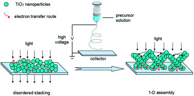
One-dimensional (1D) assembly of TiO2 nanoparticles (NPs) was successfully achieved by an improved electrospinning technique. Electrospinning precursor solution was prepared with conventional TiO2 NPs and polyvinylpyrrolidone dispersed in ethanol. The newly developed 1D assembly of nanoparticles (AS-NP) has been introduced into the photoanode in dye-sensitized solar cells (DSSCs). Compared to the traditional disordered stacking of TiO2 NPs, the AS-NPs bring in faster charge transport and longer electron lifetime, as well as a higher light scattering ability (especially in the wavelength range from 500 nm to 650 nm). It is exhibited that the AS-NPs can enhance electron transport and light scattering, while retaining the merits of NP morphology. Consequently, the efficiency of a cell based on an AS-NP/NP bilayer photoanode could be improved by about 15% in comparison to a reference cell made of absolute TiO2 NPs.


Introduction

Since the breakthrough in 1991,1 dye-sensitized solar cells (DSSCs) have attracted much research attention due to their low cost, easy preparation and multicolor options. So far, the power conversion efficiency (PCE) has been heightened to 12.3% for a DSSC under simulated air mass 1.5 global sunlight (AM 1.5G), which was attributed to the introduction of a cosensitized photoanode and a CoII/IIItris (bipyridyl)-based redox electrolyte.2 Further improvement of the performance has been tried in various other ways, two of which are increasing the optical path and enhancing photogenerated electron transport in the photoanode.3–11

A typical DSSC is composed of a porous TiO2 nanoparticle (NP) photoanode sensitized with light-absorbing dyes, a liquid electrolyte containing I/I3¬, and a Pt counter electrode. The porous NP film has the advantages of high surface area and good electrolyte permeation to obtain a considerable efficiency for DSSCs. However, photogenerated electrons recombine with oxidized species in the electrolyte before reaching the substrate, and disordered stacking of TiO2 NPs easily causes the random transmission of electrons and trapping/detrapping events along the electron's path, which aggravate the recombination and reduce the electron lifetime.12–14 Recently, one-dimensional (1D) TiO2 nanostructures such as nanofibers have been studied as photoanode materials to improve the electron mobility and charge collecting rate.15–17

The electrospinning technique is a well-established, simple and versatile method for preparation of nanofibers with diameters typically ranging from tens to hundreds of nanometers. DSSCs based on electrospun TiO2 nanofibers as the photoanode have shown substantial improvement in electron transport.18–25 However, customary electrospinning using precursor sol produces colloidal nanofibers, which crystallize after calcining at high temperature. The prepared TiO2 nanofibers have relatively small specific surface area because of their smooth surface. This is a significant disadvantage to improve the efficiency of DSSCs due to the low dye adsorption of the photoanode.

For DSSCs with good performance, the semiconductor of the photoanode should have three attributes: large surface area, fast electron mobility and good light scattering. To overcome the dilemma mentioned above, Joshi et al. reported that a composite made of electrospun TiO2 nanofibers and conventional TiO2 NPs could enhance electron transport and light scattering with slight dye uptake reduction, demonstrating higher device efficiency than those made of TiO2 NPs alone.26,27 Meanwhile, many researchers have worked on enhancing the surface roughness of nanofibers to increase the dye uptake.28 Hwang et al. demonstrated that multiscale porous TiO2 nanofibers were fabricated using an electrospinning and etching process with TiO2–SiO2 composite nanofibers.9 Lin et al. reported that wormhole-like mesoporous TiO2 nanofibers were prepared by electrospinning with ionic liquid, after which the ionic liquid was removed.29 However, these methods were inconvenient and still did not work out for the best. Further optimization of 1D TiO2 nanostructures with a large surface area by simple methods is still an important issue under research.

In this study, one-dimensional (1D) assembly of TiO2 nanoparticles (NPs) was successfully achieved by an improved electrospinning technique. The precursor solution was prepared using TiO2 NPs instead of titanium butoxide. It is indicated that the 1D assembly of TiO2 NPs (AS-NP) can overcome the disadvantages of traditional nanofibers because of the retained NP morphology. The AS-NP also brings in faster charge transport and longer electron lifetime, and at the same time shows a higher light scattering ability than traditional disordered stacking NPs. Our work demonstrates that the AS-NP has advantages of both NPs and traditional nanofibers, which have contributed to an improvement in efficiency of 15% for DSSCs compared to absolute TiO2 NPs.

Experiments

Preparation of TiO2 NPs

TiO2 NPs were synthesized as reported.30 Acetic acid (1.19 g) was added into 8 g titanium isopropoxide. After stirring at room temperature for 20 min the mixture was dropped into deionized water under vigorous stirring. 0.81 ml HNO3 (60 wt%) was added to the mixture after hydrolysis for 1 h and the resulting mixture was heated from room temperature to 80 °C evenly in 50 min. The resulting sol was transferred into a 100 ml Teflon-lined autoclave for hydrothermal treatment at 240 °C for 12 h. Afterwards, 0.34 ml HNO3 was added and the mixture was treated with an ultrasonic horn for dispersion. Finally, the prepared colloid was triply centrifuged and washed with ethanol to remove HNO3 and organics.

Electrospinning

The obtained precipitate was dispersed in 19 ml of ethanol by an ultrasonic horn for 90 min. Then 1.22 g poly vinyl pyrrolidone (PVP, Mw = 1[thin space (1/6-em)]300[thin space (1/6-em)]000) was added into the solution, followed by magnetic stirring for 30 min to form a homogeneous solution. Following this step, the mixture was placed in a plastic syringe equipped with a blunted stainless steel needle of 0.4 mm inner diameter. During the electrospinning, a positive high voltage of 15 kV was applied to the needle, a propulsion rate of 1.5 ml h−1 was maintained, and the distance between the needle tip and the collecting panel was 18 cm. The obtained PVP–NP composites were collected on an aluminum foil covered metal plate, then calcined in an air atmosphere for 6 h at 500 °C, increasing the temperature at a rate of 10 °C min¬1.

Preparation of paste

1 g of 1D assembled TiO2 NPs was dispersed in anhydrous ethanol, followed by ultrasonication. Then terpinol (2 g) and ethyl cellulose (10 wt%, 4 g) were added and the mixture was sonicated again to obtain a stabilized colloid. Finally, the colloid was concentrated with a rotary evaporator at 40 °C to get the paste. The same as above, the preparation of the absolute NP paste only differed in mass ratio (TiO2[thin space (1/6-em)]:[thin space (1/6-em)]terpinol[thin space (1/6-em)]:[thin space (1/6-em)]ethyl cellulose = 1[thin space (1/6-em)]:[thin space (1/6-em)]3[thin space (1/6-em)]:[thin space (1/6-em)]5).

Fabrication of DSSCs

Fluorine-doped tin dioxide (FTO) conductive glass with a sheet resistance of 15 Ω sq−1 was cleaned by ultrasonic washing in a detergent solution, deionized water and acetone for 20 min each in succession, then immersed in 40 mM aqueous TiCl4 at 70 °C for 20 min to be coated with a thin compact layer of TiO2. The paste was coated onto the substrate using a doctor-blade technique. After being dried at 125 °C in air, the film was annealed at 450 °C for 15 min in air. Another compact layer of TiO2 and another layer of paste were coated onto the substrate again. After being annealed at 450 °C for 15 min, the film was immersed in 40 mM aqueous TiCl4 at 70 °C for 20 min again to block the charge recombination and enhance the bonding strength between the oxide films. Then the film of double layers was sintered at 500 °C for 0.5 h in air. After being cooled to 80 °C, the film was soaked in N719 ethanol solution for 20 h at room temperature. The counter electrodes were prepared by sputtering platinum onto FTO glass. The electrolyte was composed of 1.0 M BMII, 30 mM I2, and 0.5 M tert-butylpyridine in a mixed solvent of acetonitrile and valeronitrile (v/v, 85[thin space (1/6-em)]:[thin space (1/6-em)]15).

Characterization

A FEI NOVA NanoSEM230 scanning electron microscope (SEM) and a JEOL 3010 transmission electron microscope (TEM) were employed to characterize the morphological and structural properties of all the samples. The JV testing of the DSSC sample employed a Keithley 236 source measure unit under AM 1.5 illumination cast by an Oriel 92251A-1000 sunlight simulator. The EIS measurements were carried out with a PARSTAT 2273 advanced electrochemical system (Princeton Applied Research, USA) over a frequency range of 0.5–500[thin space (1/6-em)]000 Hz under AM 1.5. The magnitude of the AC modulation signal was 10 mV. The incident photo-to-current conversion efficiency (IPCE) spectrum was collected with a self-built apparatus. A Shimadzu UV-2550 UV-vis spectrometer fitted with an integrating sphere was used to investigate the optical reflectance of the films. UV-visible reflectance spectra of powder samples were recorded using a pure BaSO4 pellet as the reference. The photoelectrode film thickness of the DSSC sample was measured by a Dektak 6M profilometer.

Results and discussion

The novel 1D assembly of TiO2 NPs was prepared by an electrospinning technique with a precursor solution of conventional TiO2 NPs and PVP dispersed in ethanol. In the preparation process, the concentrations of TiO2 NPs and PVP in the precursor solution were crucial for the 1D assembly. High concentration brought about needle blocking, while low concentration produced irregular agglomeration of NPs. Further experimental details are provided in the Experiments section.

For comparison, three films with similar thicknesses were coated onto FTO glass using a doctor-blade technique (NP, AS-NP/NP and AS-NP films with around 12 μm NPs, 6 μm NPs + 6 μm assembled NPs and 12 μm assembled NPs, respectively). Fig. 1a and c show field emission scanning electron microscopy (FESEM, NOVA NanoSEM230) images (top views) of the synthesized NP and AS-NP films, and Fig. 1b and d are the corresponding magnified FESEM images, respectively. The NP film is constructed by the disordered stacking of TiO2 NPs. Fig. 1c and d indicate that numerous 1D assemblies with diameters in the range of 150–400 nm and lengths up to a few microns cover the substrate, and look like bridges overlapping each other. The figures also reveal that these structures with rough surfaces are composed of packed TiO2 NPs. This morphology can be maintained after annealing at 500 °C for 0.5 h in air. The TEM result in Fig. 1e further shows the detailed morphological structure of the 1D assembly, which consisted of TiO2 NPs with sizes of about 10 nm. The 1D assembly meant that the TiO2 NPs were linked closer to each other than in the porous structure and this enhanced the necking between the particles. From the cross-sectional FESEM image of the AS-NP/NP electrode (Fig. 1f), it can be seen that the average thicknesses of the TiO2 NP layer and the AS-NP layer are similar at about 6 μm.


image file: c3ra47546h-f1.tif
Fig. 1 FESEM images of (a) and (b) NP TiO2 electrodes at different magnifications, and (c) and (d) AS-NP TiO2 electrodes at different magnifications. (e) TEM image indicating that the AS-NP consisted of TiO2 crystallites with sizes of ∼10 nm. (f) Cross-sectional FESEM image of the as-prepared AS-NP/NP TiO2 electrode.

To determine the effect of this 1D TiO2 assembly on the photovoltaic properties of DSSCs, we fabricated cells with NP, AS-NP/NP and AS-NP films as photoanodes sensitized by N719. Current density–voltage (JV) curves under AM1.5 (100 mW cm−2) illumination with an active area of 0.132 cm2 are presented in Fig. 2. The DSSC made with the AS-NP/NP film (cell AS-NP/NP) achieves a short-circuit current density (Jsc) of 16.54 mA cm−2 and an energy conversion efficiency (η) of 6.85%. In comparison, the DSSC with the NP film (cell NP) has Jsc and η values of 14.07 mA cm−2 and 5.96%, respectively. These results indicate that the improvement of η mainly resulted from the increase of Jsc. However, when the DSSC was made with the AS-NP film (cell AS-NP), the Jsc and η are only 11.19 mA cm−2 and 5.19%, respectively. Furthermore, the open-circuit voltages (Voc) of cells AS-NP/NP and AS-NP almost remain unchanged, but are larger than that of cell NP. It is known that Jsc is associated with the number of injected electrons, while Voc corresponds to the difference between the quasi Fermi level in the semiconductor (TiO2) under illumination and the reduction potential of the redox reaction in the electrolyte. In order to explore the causes, dye-loading measurements were performed by dye-desorption. The low performance of cell AS-NP is mainly attributed to the low Jsc induced by insufficient dye uptake. As shown in Table 1, the dye uptake of the AS-NP film is reduced by 27.7% from 2.96 to 2.14 × 10⁻⁷ mol m−2 compared to the NP film. From Fig. 1, it is inferred that the AS-NP film has less TiO2 content than the NP film of the same volume, and this may be the reason for the lower dye uptake.


image file: c3ra47546h-f2.tif
Fig. 2 JV curves of the DSSCs with NP, AS-NP/NP and AS-NP electrodes.
Table 1 Dye uptake and EIS data of the NP, AS-NP/NP and AS-NP electrodes
Sample Amount of absorbed dye per unit surface areaa (10−7 mol m−2) R ct (Ω) τ e (ms)
a Desorbed from the electrode by NaOH solution.
NP 2.96 5.95 15.8
AS-NP/NP 2.69 3.57 26.1
AS-NP 2.14 5.26 43.1


To analyze the cell performance in more detail, the incident photon-to-current conversion efficiency (IPCE) was measured as a function of wavelength from 380 nm to 800 nm under monochromator illumination. The maxima of the IPCE at approximately 525 nm is attributed to the dye absorption of N719. As shown in Fig. 3, the IPCE of cell AS-NP is found to be the lowest, which is in good accordance with the JV measurement and dye uptake. Compared to cell NP, the IPCE of cell AS-NP/NP increased from 71% to 79% at around 525 nm. Moreover, it is interesting that the IPCE of cell AS-NP/NP is slightly lower than that of cell NP in the short spectral range of 380–500 nm (due to the lower dye uptake), but higher than that of cell NP in the long spectral range between 520 and 800 nm.


image file: c3ra47546h-f3.tif
Fig. 3 IPCE spectra of the DSSCs with NP, AS-NP/NP and AS-NP photoanodes.

As is known, the IPCE is determined by three partial efficiencies, the light harvesting efficiency (ηLH), the electron injection efficiency (ηINJ) and the charge collection efficiency (ηCOL), and can be expressed as follows:31,32

 
IPCE(λ) = ηLH(λ)ηINJ(λ)ηCOL(λ)(1)

Normally, ηINJ is approximately the same for high performance DSSCs with TiO2 photoanodes and N719 dye. IPCE can be simplified as the product of ηLH and ηCOL. It seems a reasonable hypothesis that the variation trend of ηCOL in cells AS-NP/NP and NP is similar over the wavelength range from 380 to 800 nm, so this phenomenon should be attributed to ηLH.

TiO2 nanofibers have been proven to possess high diffuse reflection capacities, and Joshi et al. indicated that 1D nanostructures with diameters of more than 200 nm became substantially stronger at visible wavelengths by theoretical simulation.26–28 In order to investigate the light-scattering property of these films, the UV-vis reflectance spectra over the range from 380 to 800 nm was characterized and it is shown in Fig. 4. The reflectance capacities of the AS-NP and AS-NP/NP films are similar at about 30% in the short spectral range of 380–500 nm, which is slightly higher than the 20% reflectance of the NP film. But from the 500 nm wavelength, the reflectances of the AS-NP and AS-NP/NP films increase drastically to about 50% at 650 nm, while that of the NP film is almost unchanged until 650 nm. This phenomenon is coincident with the variation tendency in IPCE over the same wavelength band. These AS-NPs exhibit higher diffuse reflection capabilities in the near-infrared region than in the short-wavelength region. The better light-harvesting efficiency in the near-infrared region is likely given rise by Mie scattering due to the larger diameter of AS-NP.33 The improved diffuse reflection capabilities of the 1D assembly further indicate this structure links the TiO2 NPs closer together and enhances the light scattering.


image file: c3ra47546h-f4.tif
Fig. 4 UV-vis reflectance spectra of the NP, AS-NP/NP and AS-NP films.

In DSSCs, two factors influence the electron transport in the photoanode. One is the electron mobility and the nanostructure of the materials. For example, the mobility of bulk TiO2 is about two orders higher than that of nanocrystalline TiO2.6–11,26–28 The other is the injected electron concentration in the photoanode. The electric field in nanocrystalline TiO2 is generally considered to be negligible, so electron transport appears to occur predominantly by diffusion.34,35 As a consequence, the electron transport rate increases with the concentration of electrons. We analysed the electron transport/transfer process at the interface in the DSSCs using the electrochemical impedance spectroscopy (EIS) method. As shown in Fig. 5a, there are two semicircles from high to low frequency, corresponding to the electron transfer resistance on the Pt/electrolyte interface (Rt) and the charge transport resistance on the TiO2/dye/electrolyte interface (Rct), respectively. In addition, the high-frequency intercept on the real axis represents the series resistance, Rs.36–38 The fitting value of Rct (summarized in Table 1) corresponding to cell AS-NP/NP is the lowest due to the higher electron concentration induced by light scattering. The Rct of cell AS-NP is lower than that of cell NP in spite of the low electron concentration, reflecting that the 1D assembly accelerates the electron transfer process in the electrode. The lifetime of electrons (τe) in the oxide film can be estimated from the relation:

 
τe = 1/ωmax = 1/(2πfmax)(2)
where fmax is the maximum frequency of the impedance semicircle arc at the middle frequencies. As shown in Fig. 5a, the fmax are located at 3.7 Hz for cell AS-NP, 6.1 Hz for cell AS-NP/NP and 10.1 Hz for cell NP, respectively. The electron lifetime (τe) for recombination are thus estimated to be 43.1 ms, 26.1 ms and 15.8 ms. From Fig. 5b, it is also seen that fmax has an obvious red-shift with increasing AS-NP, which suggests the introduction of the AS-NP structure favors electron transfer and reduces the electron recombination rate effectively.


image file: c3ra47546h-f5.tif
Fig. 5 (a) Nyquist plots of EIS spectra and (b) Bode phase of the DSSCs with NP, AS-NP/NP and AS-NP electrodes, the inset is the corresponding equivalent circuit of EIS.

As reported previously, there exist two different modes of electron transport in photoanodes: the random electron walking among disordered stacking TiO2 NPs and 1D electron diffusion along nanofibers. It is usually believed that 1D charge transport is more facile than within a random NP network because electrons in nanofibers do not have to cross many particle boundaries where surface states (electron traps) are mainly located. The charge transfer in the TiO2 NP films of DSSCs is governed by the exponential distribution of surface states,39,40 and the surface states can not only exchange electrons with the conduction band of TiO2 but also recombine electrons to oxidize species in the electrolyte. Therefore, the electron lifetime is strongly influenced by the density of trapping states (DOS) amongst the TiO2 films. The 1D assembly of TiO2 NPs links the TiO2 NPs closer to each other, and the random walking of electrons is partly substituted by 1D electron diffusion. Therefore, the longer electron lifetime, τe, of cell AS-NP compared to that of cell NP should be ascribed to the decreased number of surface states participating in charge transfer. The enhanced electron transport also results in the rise of quasi Fermi level in the TiO2 film, which gives rise to the higher Voc of cell AS-NP, as shown in Fig. 6.


image file: c3ra47546h-f6.tif
Fig. 6 Energy diagram of the proposed mechanisms for electron transfer.

Conclusion

An improved electrospinning method was developed for the 1D assembly of TiO2 NPs. Inspired by the unique structure, the cell with the AS-NP/NP bilayer demonstrates a higher photoconversion efficiency of 6.85%, a 15% improvement compared to the cell made of absolute TiO2 NPs, mainly attributed to the enhanced light harvesting via improved light scattering and longer electron lifetime. It is exhibited that the 1D assembly of NPs can enhance electron transport and light scattering while retaining the merits of NP morphology. This method may have good potential for applications in DSSCs and many other related fields.

Acknowledgements

This work was supported primarily by the National Natural Science Foundation of China (11174129 and 61377051), the National Basic Research Program of China (2011CB933303 and 2013CB632404), and the Science and Technology Research Program of Jiangsu Province (BK2011056, BE2012089 and BK20130053). We thank Dr Honglin Gao for the UV-vis reflectance spectra characterization and Dr Wenguang Tu for the English modification.

Notes and references

  1. B. O'Regan and M. Grätzel, Nature, 1991, 353, 737 CrossRef.
  2. A. Yella, H. W. Lee, H. N. Tsao, C. Yi, A. K. Chandiran, M. K. Nazeeruddin, E. W. G. Diau, C. Y. Yeh, S. M. Zakeeruddin and M. Grätzel, Science, 2011, 334, 629 CrossRef PubMed.
  3. W. Q. Wu, B. X. Lei, H. S. Rao, Y. F. Xu, Y. F. Wang, C. Y. Su and D. B. Kuang, Sci. Rep., 2013, 3, 1352 Search PubMed.
  4. J. Burschka, V. Brault, S. Ahmad, L. Breau, M. K. Nazeeruddin, B. Marsan, S. M. Zakeeruddin and M. Grätzel, Energy Environ. Sci., 2012, 5, 6089 Search PubMed.
  5. G. Zhu, L. K. Pan, J. Yang, X. J. Liu, H. C. Sun and Z. Sun, J. Mater. Chem., 2012, 22, 24326 RSC.
  6. D. Hwang, H. Lee, Y. Seo, D. Kim, S. M. Jo and D. Y. Kim, J. Mater. Chem. A, 2013, 1, 1359 Search PubMed.
  7. L. J. Yang and W. W.-F. Leung, Adv. Mater., 2013, 25, 1792 CrossRef PubMed.
  8. J. Y. Zhang, J. J. Wang, Z. Y. Zhao, T. Yu, J. Y. Feng, Y. J. Yuan, Z. K. Tang, Y. H. Liu, Z. S. Li and Z. G. Zou, Phys. Chem. Chem. Phys., 2012, 14, 4763 RSC.
  9. S. H. Hwang, C. Kim, H. Song, S. Son and J. Jang, ACS Appl. Mater. Interfaces, 2012, 4, 5287 Search PubMed.
  10. D. Hwang, S. M. Jo, D. Y. Kim, V. Armel, D. R. Macfarlane and S.-Y. Jang, ACS Appl. Mater. Interfaces, 2011, 3, 1521 Search PubMed.
  11. A. S. Nair, P. Zhu, V. J. Babu, S. Yang, T. Krishnamoorthy, R. Murugan, S. Peng and S. Ramakrishna, Langmuir, 2012, 28, 6202 CrossRef PubMed.
  12. J. A. Anta, Energy Environ. Sci., 2009, 2, 387 Search PubMed.
  13. J. Bisquert, F. F. Santiago, I. M. Seró, G. G. Belmonte and S. Giménez, J. Phys. Chem. C, 2009, 113, 17278 Search PubMed.
  14. J. P. G. Vazquez, J. A. Anta and J. Bisquert, J. Phys. Chem. C, 2010, 114, 8552 Search PubMed.
  15. B. Tan and Y. Y. Wu, J. Phys. Chem. B, 2006, 110, 15932 CrossRef PubMed.
  16. G. K. Mor, K. Shankar, M. Paulose, O. K. Varghese and C. A. Grimes, Nano Lett., 2006, 6, 215 CrossRef PubMed.
  17. H. Kokubo, B. Ding, T. Naka, H. Tsuchihira and S. Shiratori, Nanotechnology, 2007, 18, 165604 CrossRef.
  18. H. Krysova, A. Zukal, J. Trckova-Barakova, A. K. Chandiran, M. K. Nazeeruddin, M. Grätzel and L. Kavan, Chimia, 2013, 67, 149 CrossRef PubMed.
  19. N. M. Tikekar and J. J. Lannutti, Ceram. Int., 2012, 38, 4057 CrossRef PubMed.
  20. X. W. Huang, J. Y. Deng, L. Xu, P. Shen, B. Zhao and S. T. Tan, Acta Chim. Sin., 2012, 70, 1604 CrossRef.
  21. Y. Li, D. K. Lee, J. Y. Kim, B. Kim, N. G. Park, K. Kim, J. H. Shin, I. S. Choi and M. J. Ko, Energy Environ. Sci., 2012, 5, 8950 Search PubMed.
  22. M. Zukalova, L. Kavan, J. Prochazka, A. Zukal, J. H. Yum and M. Grätzel, J. Nanopart. Res., 2013, 15, 1640 CrossRef.
  23. G. F. He, Y. B. Cai, Y. Zhao, X. X. Wang, C. L. Lai, M. Xi, Z. T. Zhu and H. Fong, J. Colloid Interface Sci., 2013, 398, 103 CrossRef PubMed.
  24. G. F. He, X. X. Wang, M. Xi, F. Zheng, Z. T. Zhu and H. Fong, Mater. Lett., 2013, 106, 115 CrossRef CAS PubMed.
  25. M. Hamadanian and V. Jabbari, Int. J. Green Energy, 2014, 11, 364 CrossRef CAS.
  26. P. Joshi, L. F. Zhang, D. Davoux, Z. T. Zhu, D. Galipeau, H. Fong and Q. Q. Qiao, Energy Environ. Sci., 2010, 3, 1507 CAS.
  27. X. X. Wang, S. Karanjit, L. F. Zhang, H. Fong, Q. Q. Qiao and Z. Zhu, Appl. Phys. Lett., 2011, 98, 082114 CrossRef PubMed.
  28. S. F. Zhang, X. D. Yang, Y. H. Numata and L. Y. Han, Energy Environ. Sci., 2013, 6, 1443 CAS.
  29. Y. P. Lin, Y. Y. Chen, Y. C. Lee and Y. W. C. Yang, J. Phys. Chem. C, 2012, 116, 13003 CAS.
  30. X. G. Han, Q. Kuang, M. S. Jin, Z. X. Xie and L. S. Zheng, J. Am. Chem. Soc., 2009, 131, 3152 CrossRef CAS PubMed.
  31. M. Grätzel, Inorg. Chem., 2005, 44, 6841 CrossRef PubMed.
  32. G. G. Xue, X. R. Yu, T. Yu, C. X. Bao, J. Y. Zhang, J. Guan, H. Huang, Z. K. Tang and Z. G. Zou, J. Phys. D: Appl. Phys., 2012, 45, 425104 CrossRef.
  33. H. J. Koo, J. Park, B. Yoo, K. Kim and N. G. Park, Inorg. Chim. Acta, 2008, 361, 677 CrossRef CAS PubMed.
  34. L. M. Peter and K. G. U. Wijayantha, Electrochim. Acta, 2000, 45, 4543 CrossRef CAS.
  35. A. C. Fisher, L. M. Peter, E. A. Ponomarev, A. B. Walker and K. G. U. Wijayantha, J. Phys. Chem. B, 2000, 104, 949 CrossRef CAS.
  36. J. Halme, P. Vahermaa, K. Miettunen and P. Lund, Adv. Mater., 2010, 22, 210 CrossRef PubMed.
  37. J. Qian, P. Liu, Y. Xiao, Y. Jiang, Y. Cao, X. Ai and H. Yang, Adv. Mater., 2009, 21, 3663 CrossRef CAS.
  38. Z. D. Li, Y. Zhou, T. Yu, J. G. Liu and Z. G. Zou, CrystEngComm, 2012, 14, 6462 RSC.
  39. J. Bisquert, F. F. Santiago, I. M. Seró, G. G. Belmonte and S. Giménez, J. Phys. Chem. C, 2009, 113, 17278 CAS.
  40. Q. Wang, S. Ito, M. Grätzel, F. F. Santiago, I. M. Ser, J. Bisquert, T. Bessho and H. Imai, J. Phys. Chem. B, 2006, 110, 25210 CrossRef CAS PubMed.

This journal is © The Royal Society of Chemistry 2014