DOI:
10.1039/C3RA47420H
(Paper)
RSC Adv., 2014,
4, 13788-13795
Photophysical and photoconductivity properties of thiol-functionalized graphene–CdSe QD composites†
Received
9th December 2013
, Accepted 30th January 2014
First published on 31st January 2014
Abstract
Graphene–semiconductor QD hybrid nanostructure materials have recently emerged as a new class of functional materials because of their potential applications in solar energy conversion, optoelectronic devices, sensing etc. Here, oleic acid-capped CdSe QDs are attached to –PhSH functionalized graphene by ligand exchange via bonding with the –SH group. The shifting of the G-band and D-band due to structural changes for the attachment of QD with graphene has been evaluated by using Raman spectroscopy. Steady state photoluminescence (PL) and time resolved fluorescence measurements have been employed to understand the electronic interactions between graphene and CdSe QDs. A time resolved fluorescence spectroscopic study has been used to understand the fluorescence dynamics of the photoexcitated CdSe QDs in the presence of graphene. It is evident that the electron transfer occurs from photoexcited QDs to graphene and the electron transfer rate is found to be 12.8 × 10⁸ s−1 for 3.8 nm CdSe QDs. Photoconductivity properties of the graphene–QD device under illumination have been examined and it is to be noted that 2–3 fold increase in the photocurrent is found in this composite device in presence of 1.5 AM solar simulated light. The enhancement of the photocurrent in this hybrid device is found to be suitable for potential applications in optoelectronic and solar cell systems.
1. Introduction
The two dimensional single atomic carbon sheet of graphene has emerged as an attractive material1 for its unique properties, like the quantum Hall effect at room temperature, ballistic transport behavior due to the availability of particles like Dirac fermions2 and excellent tensile strength (1 TPa).3 Ideal, single layer graphene possesses extremely high mobility of charge carriers (electrons or holes) and is a transparent semi-metal because it absorbs only ∼2% of the visible light.1,4 These properties make graphene a promising candidate for use in ultrafast photodetectors,5 chemical sensing,6 high-speed electronics,7 thermal management8 and solar cells.9,10 The successful tuning of the graphene surface to make it either electron or hole rich by applying a suitable gate voltage has been reported.11 The presence of metal ions or adsorbed molecules has also been found to be very effective in causing a shift of the graphene’s Fermi level with precise control.6,12 On the other hand, the electronic interaction of graphene with electron donor/acceptor molecules or nanoparticles has been found to be interesting because of the resulting significant modification in the electronic structures and properties of graphene. It is evident that quantum dots (QDs) are becoming increasingly important because of their broad and size tunable absorption13 and multi-exciton generation,14 facilitating higher theoretical efficiencies than that prescribed by the Schockley–Quiesser limit.15 The key to the successful utilization of the optical properties of CdSe QDs requires them to be in intimate contact with a conducting medium which can give rise to type II band alignment with the CdSe QDs.16 The Fermi level of graphene lies between −4.42 eV to −4.5 eV, which is well below the conduction band of CdSe QDs (−3.5 to −4 eV). Thus, the photoexcited electron of a CdSe QD may be injected into the graphene Fermi level.17 In spite of several reports on graphene–CdSe QD hybrids,17,18 the basic understanding of relaxation of excited CdSe QDs in presence of graphene is still under debate. Brus et al.19 have reported that excited CdSe/ZnS (core–shell) QDs decay by energy transfer (by Förster Resonant Energy Transfer mechanism) to pristine graphene. It is reported also that the electron transfer process can dominate over energy transfer during the chemical interactions between CdSe QDs and graphene. Bang and Kamat have reported a CdSe QD–fullerene hybrid nanocomposite by chemically linking QDs with thiol-functionalized C60 for solar energy conversion.20
Similarly, in the present study, oleic acid capped QDs are attached to –PhSH pre-functionalized graphene by ligand exchange in order to get bonded to the –SH groups (acting as chemical anchors, Scheme 1). The structural changes due to the attachment of the QDs have been evaluated by using Raman spectroscopy. Steady state photoluminescence (PL) and time resolved fluorescence measurements are used to understand the electronic interactions between graphene and the CdSe QDs. Time resolved spectroscopy reveals the electron transfer process from the photoexcited QDs to the graphene. The transport properties of the graphene–QD device under visible light illumination have been investigated. Photocurrent measurements of this device open up a new avenue in solar energy conversion, photovoltaic and optoelectronic applications.
 |
| | Scheme 1 Ligand exchange of CdSe QDs (oleic acid-capped) with the –SH group on f-FLG (or RGO-SH). The phenyl group (−Ph) mediates the electron transfer from excited CdSe to graphene. | |
2. Experimental section and characterization
Materials
Graphite powder, sodium dodecylsulphonate (SDS), NaBH4 and 4-aminothiophenol were purchased from Aldrich and used as received. H2SO4 (98%), HNO3 (63%), HCl (38%), NaNO2, H2O2 were received from Thomas Baker and used without further purification. PTFE filter paper was obtained from Rankem. MilliQ water (DI water) was used for all purposes unless otherwise stated. Toluene and dimethylformamide (DMF) were purchased from MERCK.
Synthesis of –PhSH terminated graphene and the exchange of CdSe QDs. For the synthesis of –PhSH terminated graphene and subsequent CdSe attachment, we followed the same strategy adopted in our recent work.21 Briefly, 0.1 g graphene oxide (GO) was suspended in water using sonication for 15 min followed by reduction with NaBH4 (1![[thin space (1/6-em)]](https://www.rsc.org/images/entities/char_2009.gif) :3 wt ratio) for 12 h to obtain chemically converted graphene (CCG) or reduced graphene oxide (RGO, mentioned here onwards as few layer graphene or FLG). Subsequently, the mixture was filtered through a 0.4 μm PTFE filter and washed thoroughly with DI water. This FLG was then re-suspended in 0.1 wt% sodium dodecylsulphonate (SDS) aq. solution. A diazonium salt of 4-aminothiophenol (4-ATP) was prepared by mixing 70 mg 4-ATP with 200 mg NaNO2 in 40 ml distilled water at 0–5 °C followed by the addition of 3 ml 6 M HCl solution (ice cold) slowly to the above mixture. A gradual change of the solution color from opaque to transparent pale yellow indicated the formation of diazonium salt. The mixture was then slowly (and with constant stirring) added to the RGO suspension (at 0–5 °C) and allowed to stir for another 4 h. Subsequently, the reaction mixture was filtered, washed with DI water and re-suspended in DMF to remove the SDS surfactant and excess unreacted 4-ATP molecules. The suspension was finally filtered and washed to get –Ph–SH functionalized FLG (f-FLG). Previously prepared oleic acid-capped CdSe QDs (CdSe–OA) (concentration of CdSe suspension was maintained by fixing the first excitonic peak intensity at 0.1 optical density throughout all our experiments) were then exchanged by mixing the DMF suspension of f-FLG (12.7 mg ml−1) with toluene soluble CdSe–OA. The hybrid was then obtained by centrifugation at 3000 rpm for 5 min followed by repeated washing with toluene and ethanol. This hybrid was then drop casted onto a copper grid for transmission electron microscopy (TEM) and coated on Si/SiO2 (200 nm SiO2) for Raman analysis, while optical measurements were carried out in solution.
:3 wt ratio) for 12 h to obtain chemically converted graphene (CCG) or reduced graphene oxide (RGO, mentioned here onwards as few layer graphene or FLG). Subsequently, the mixture was filtered through a 0.4 μm PTFE filter and washed thoroughly with DI water. This FLG was then re-suspended in 0.1 wt% sodium dodecylsulphonate (SDS) aq. solution. A diazonium salt of 4-aminothiophenol (4-ATP) was prepared by mixing 70 mg 4-ATP with 200 mg NaNO2 in 40 ml distilled water at 0–5 °C followed by the addition of 3 ml 6 M HCl solution (ice cold) slowly to the above mixture. A gradual change of the solution color from opaque to transparent pale yellow indicated the formation of diazonium salt. The mixture was then slowly (and with constant stirring) added to the RGO suspension (at 0–5 °C) and allowed to stir for another 4 h. Subsequently, the reaction mixture was filtered, washed with DI water and re-suspended in DMF to remove the SDS surfactant and excess unreacted 4-ATP molecules. The suspension was finally filtered and washed to get –Ph–SH functionalized FLG (f-FLG). Previously prepared oleic acid-capped CdSe QDs (CdSe–OA) (concentration of CdSe suspension was maintained by fixing the first excitonic peak intensity at 0.1 optical density throughout all our experiments) were then exchanged by mixing the DMF suspension of f-FLG (12.7 mg ml−1) with toluene soluble CdSe–OA. The hybrid was then obtained by centrifugation at 3000 rpm for 5 min followed by repeated washing with toluene and ethanol. This hybrid was then drop casted onto a copper grid for transmission electron microscopy (TEM) and coated on Si/SiO2 (200 nm SiO2) for Raman analysis, while optical measurements were carried out in solution.Optical absorption spectra were taken at room temperature using a UV-Vis spectrophotometer (SHIMADZU) and the sizes of CdSe QDs are calculated to be 3.03 nm, 3.80 nm and 4.70 nm. Room temperature photoluminescence spectra were recorded by a Fluoromax-P (HORIBA JOBIN YVON) spectrophotometer. Photoluminescence quantum yields (QY) for CdSe QDs were obtained by comparison with reference dye (rhodamine 6 G in water), using the following equation:
| | |
QYs = (Fs × Ar × ns2 × QYr)/(Fr × As × nr2)
| (1) |
where
Fs and
Fr are the integrated fluorescence emission of the sample and the reference respectively.
As and
Ar are the absorbance at the excitation wavelength of the sample and the reference and QY
s and QY
r are the quantum yields of the sample and the reference (QY
r = 95%).
22 The refractive indices of the solvents used for the preparation of the sample (in toluene) and reference (in water) are given by
ns (1.49) and
nr (1.33) respectively. The values of
Fs and
Fr were determined from the photoluminescence spectra corrected for the instrumental response, by integrating the emission intensity over the desired spectral range. Only the band edge luminescence peak was integrated (any other luminescence bands, such as defect associated luminescence or solvent fluorescence were discarded as background). For the time correlated single photon counting (TCSPC) measurements, the samples were excited at 375 nm using a nano-second diode laser (IBH Nanoled) in an IBH Fluorocube apparatus. The typical full width at half-maximum (FWHM) of the system response using a liquid scatter was about 300 ps. The repetition rate was 1 MHz. The fluorescence decays were analyzed using IBH DAS6 software. The following equation was used to analyze the experimental time resolved fluorescence decays,
23 P(
t)
| |
 | (2) |
Here,
n is the number of discrete emissive species,
b is a baseline correction (“dc” offset), and
αi and
τi are pre-exponential factors and excited-state fluorescence lifetimes associated with the
ith component, respectively. For multi-exponential decays the average lifetime,〈
τ〉, was calculated from the following equation,
24| |
 | (3) |
where

and
ai is the contribution of the
ith decay component. All Raman spectroscopy measurements were carried out at room temperature (298 K) on an HR 800 Raman spectrophotometer (Jobin Yvon HORIBA, France) using monochromatic radiation emitted by an Ar
+ laser (514 nm), operating at 20 mW. A 50x long distance objective lens was used for the experiment and the laser power on the sample was kept at ∼0.8 mW to avoid heating effects. The experiment was repeated several times and in several places to verify the consistency of the spectra. Transmission Electron Microscopy (TEM) was carried out using a G2 Tecnai F30 operated at an accelerating voltage of 300 kV with a resolution of 0.147 nm. X-ray photoelectron spectroscopic (XPS) measurements were carried out on a VG Micro Tech ESCA 3000 instrument at a pressure of >1 × 10
−9 Torr (pass energy of 50 eV with an electron take off angle of 60° and an overall resolution of 1 eV) using Mg Kα (source,
hν = 1253.6 eV) radiation. The alignment of the binding energy (BE) was carried out using Au 4f binding energy of 84 eV as the reference. The X-ray flux (power 70 W) was kept deliberately low in order to reduce the beam-induced damage. The spectra were fitted using a combined polynomial and Shirley-type background function.
25
For the photoconductivity study, the CdSe–f-FLG(SH) hybrid was spray coated on fluorine-doped tin oxide-coated glass substrates (FTO) at 70–80 °C until a desired thickness (∼200 nm) was reached. Then a thin layer of PEDOT:PSS (∼70–80 nm) was coated on a pretreated indium tin oxide-coated glass substrate (ITO) by spin coating from aqueous solution. The two electrodes were then put together on top of one another and clipped (so as to increase adhesion) (flip-chip) while the PEDOT:PSS coating was still wet. The resulting device was then annealed at 120 °C under an argon atmosphere for 30 min. After cooling to room temperature, the device was tested for I–V measurement. The I–V measurement was carried out by sweeping the potential at 20 mV s−1 using a BioLogic SP300 potentiostat both in dark as well as in presence of 1.5 AM solar simulated light (100 mW cm−2). A bias was applied to FTO with respect to ITO. The active area of the device was kept as 0.56 cm−2 in all cases.
3. Results and discussion
TEM analysis
Fig. 1(a–d) displays low and high resolution transmission electron microscopy (HRTEM) images of f-FLG and f-FLG–CdSe QD (4.7 nm) hybrids. Images for the hybrids were taken of the samples containing 0.268 mg ml−1 of f-FLG. Interestingly, the low magnification image shows complete coverage of the QDs on the f-FLG (Fig. 1(b)) as compared to only f-FLG, in which case no CdSe QD is visible. After exchange with the thiol groups on FLG, the CdSe QDs form an almost complete monolayer coverage on FLG at this concentration of f-FLG. The FFT in the inset of Fig. 1(d) indicates the formation of cubic CdSe and the d-spacing (2.9 Å) matches well with the literature report. The attachment of the QDs on the graphene surface has been confirmed by the TEM images.
 |
| | Fig. 1 High resolution TEM images of f-FLG and f-FLG (0.268 mg ml−1)–CdSe QDs (4.7 nm). (a) Only f-FLG and (b) f-FLG–CdSe hybrids at low magnification, (c) and (d) high magnification images of f-FLG–CdSe hybrids. Inset of (d) shows the reduced FFT pattern of the QDs. | |
XPS characterization
XPS of f-FLG–CdSe (4.7 nm) was carried out in order to validate the presence of the thiol group as well as its binding to the CdSe QDs (4.7 nm) mainly by analyzing the carbon (C 1s), and sulphur (S 2p) as well as cadmium (Cd 3d) spectra recorded using this f-FLG–CdSe (4.7 nm) hybrid. Accordingly, Fig. 2(a)–(c) show typical core level XP spectra of carbon, cadmium and sulphur of the hybrid. The cadmium (in the form of CdSe) (Fig. 2(b)) signal could be fitted quite well with a single spin-orbit pair at 405.3 eV (3d5/2) and 412 eV (3d3/2). These values are in good agreement with those reported for TOPO-capped CdSe QDs.26 Similarly, S2p core level spectrum (Fig. 2(c)) could be deconvoluted to two peaks at 163.4 eV and 166.7 eV. The first peak (163.4 eV) corresponds to the S atoms of the –PhSH groups, bonded to the CdSe QDs. The peak at a higher binding energy (166.7 eV) is associated with the presence of some amount of S-atoms at a higher oxidation state (S6+), formed during the sample preparation and exposure to X-rays, as has been observed previously.27 Binding to CdSe renders the S-atom (of –SH group) more electronegative and hence produces the consequent blue shift of the binding energy of sulphur as compared to S in the normal –SH group (161–162 eV). This value of binding energy (B.E) (for CdSe-thiol bonding) is in excellent agreement with the reported B.E value for the S 2p signal in case of self-assembled monolayers of alkanethiols and aromatic thiols, as well as alkanethiol-capped silver nanoparticles.28–30 This reveals that in the homogeneous mixture of CdSe QDs (in toluene) and f-FLG (in DMF), the CdSe QDs are chemically bonded to f-FLG surface due to ligand exchange between the thiol group and oleic acid. As no peak for carbon-sulphur binding (164 eV according to literature31) is observed in the spectrum, the 4-ATP molecule is expected to be bonded through a C–C linkage to graphene and not through a C–S bond. The C1s Fig. 2(a) signal also agrees well with this explanation. The C1s signal can be de-convoluted to 4 different peaks. The low B.E peak at 284.1 eV corresponds to sp2 carbons from the graphene (f-FLG) surface and the peak at 284.9 eV is due to sp3 carbons resulting from a covalent binding of the graphene surface. Higher B.E peaks at 286 eV and 288 eV indicate the attachment of carbons to more electronegative elements like oxygen and sulphur. However, the intensity and the area of this high B.E peak are very small as compared to the rest of the peaks, which suggests that the amount of higher oxidation sulphur species (S6+) is very small. XPS study further confirms the covalent binding of CdSe QDs on the graphene surface.
 |
| | Fig. 2 Core level XPS spectra of (a) carbon (C 1s), (b) cadmium (Cd 3d) and (c) sulphur (S 2p) spectra of the f-FLG–CdSe (4.7 nm) hybrid. | |
Raman study
The structural change of graphene due to the attachment of the QDs on the graphene surface has been investigated by Raman spectroscopy. Fig. 3 is a comparison of the representative Raman spectra of the FLG, f-FLG and the f-FLG–CdSe QDs hybrid (CdSe-4.7 nm) excited with a 514 nm Ar+ laser. The phonon mode vibration at 1338 cm−1 is a symmetry-forbidden band, named as the D-band or defect-induced band because the presence of defects breaks the translational symmetry and hence the transition occurs (breathing mode of the k-point phonons of the A1g symmetry). The band at 1596 cm−1 is the long wavelength longitudinal phonon mode of graphene (E2g phonon), named as the G-band or graphitic band arising due to the sp2 carbon network of the graphene plane.32 However, both the D and G band positions remain unaffected after thiol (–SH) functionalization of the FLG (or RGO), but both bands are shifted to a lower energy after CdSe QDs attachment. This red shift (equivalent to ∼0.8 meV) implies a softening of the phonons of the FLG due to electron accumulation on the graphene.27 A similar effect has been observed in the case of molecular doping in graphene in the presence of an electron donor like tetrathiafulvalene (TTF).27 In that case, a shift of ∼10 cm−1 led to a doped electron concentration of ∼1012 cm−2 for 0.1 M TTF in graphene. The Fermi level of graphene (−4.5 eV) matches well the conduction band positions of these QDs (−3.3 to −3.4 eV for change in particle size from 3.8 nm to 4.7 nm). Therefore, the excited electrons can be transferred to graphene and this becomes electron rich which causes a softening of the phonons (analogous to electron enrichment in CNTs).33 Interestingly, the ID to IG ratio (1.09 for hybrid, 1.15 for f-FLG, 1.10 for FLG in this case) remains almost the same for all the three cases. This reveals that the nature and amount of defects remains the same before and after functionalization of the graphene surface. Other than the D- and G-bands, the Raman spectra of the hybrid materials also bear the features of the CdSe QDs in the 100–500 cm−1 region (ESI, Fig. S1†) which is absent in the case of both FLG and f-FLG. The peak at 201–202 cm−1 is attributed to the longitudinal optical (LO) phonon mode of CdSe34 and the appearance of the LO peak within 201–202 cm−1 as compared to 210 cm−1 for bulk CdSe, demonstrates the size quantization effects.35 The structural changes due to the attachment of QDs to the graphene surface is thereby confirmed by Raman study.
 |
| | Fig. 3 Room temperature (298 K) micro Raman spectra of (a) FLG, (b) f-FLG and (c) CdSe-f–FLG hybrids (CdSe-4.7 nm) obtained using a 514 nm Ar+ laser using 50× objective (spot size ∼1.14 μm). Samples were coated on a SiO2-coated Si-wafer for better resolution and to get rid of the effect of fluorescence. The black dotted lines are a guide to the eye. | |
Steady state and time-resolved spectroscopic study
Fig. 4(A) shows a comparison of the absorption spectra of three different sizes (3.03 nm, 3.80 nm and 4.70 nm) of oleic acid-capped CdSe QDs. The position of the first electronic transition is shifted to higher photon energies (blue shift) with decreasing the particle size, which is consistent with previous results.36,37 Fig. 4(B) shows the photoluminescence (PL) emission spectra of the corresponding CdSe QDs. Furthermore, the quantum yields (QYs) of the CdSe QDs have been calculated to be 8.80%, 14.93% and 11.52% for 3.03, 3.80 and 4.70 nm CdSe QD, respectively. It is noted that the QY of the 3.8 nm size CdSe QDs is found to be higher.
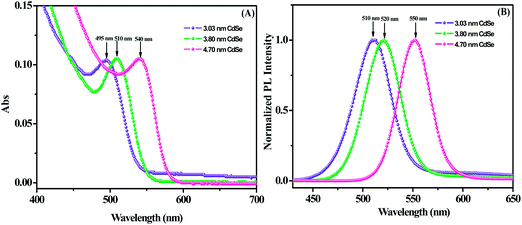 |
| | Fig. 4 (A) Absorption and (B) photoluminescence spectra of the CdSe QDs capped with oleic acid in toluene. | |
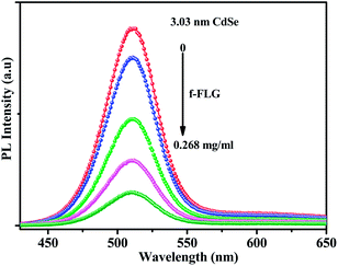
Fig. 5 shows the photoluminescence spectra of 3.03 nm CdSe before and after the attachment. Photoluminescence intensity of CdSe is effectively quenched by f-FLG and the PL intensity decreases with increasing f-FLG content. The calculated PL quenching efficiency increases from 14.35% to 82.26% with increasing the f-FLG concentration from 0.036 to 0.268 mg ml−1. In case of 3.80 nm and 4.70 nm CdSe QDs, the PL quenching efficiencies are 84.25% and 82.00% for an f-FLG concentration of 0.268 mg ml−1. The photoluminescence spectra of 3.8 nm and 4.7 nm CdSe QDs–f-FLG are given in the ESI (Fig. S2 and S3†). The photoluminescence quenching of CdSe QDs is indicative of the electronic interactions between the excited state of the CdSe and the f-FLG.
 |
| | Fig. 5 Photoluminescence spectra of CdSe before and after the attachment of a controlled amount of f-FLG (excitation source 375 nm). | |
To confirm the energy/electron transfer process from the QDs to graphene, a time resolved fluorescence study is performed which is more sensitive than the PL quenching study. Fig. 6 shows the photoluminescence decay curves of 3.03 nm CdSe QDs as a function of increasing concentration of f-FLG at the excitation and emission wavelengths of 375 nm and 510 nm, respectively. All the decay curves are fitted with tri-exponential functions. The decay components of the pure 3.03 nm CdSe QDs are 0.76 ns (58.4%), 7.70 ns (27.4%) and 39.29 ns (14.2%) and the average decay time is 8.13 ns using eqn (3). In the presence of the highest concentration of f-FLG (0.268 mg ml−1), the corresponding components are 0.57 ns (74.5%), 6.48 ns (18.2%) and 38.49 ns (7.3%) and the average decay time is 4.41 ns. The fluorescence decay time of the CdSe QDs decreases with the increasing concentration of f-FLG, which is consistent with the fluorescence results. With increasing the f-FLG concentration, the fast component (τ1) decreases from 0.76 ns to 0.57 ns over the f-FLG concentration range of 0.036–0.268 mg ml−1 but slow components (τ2 and τ3) decrease negligibly (Table 1). The contribution of the fast component increases from 58.8% to 74.5% and the contribution of slow components decreases from 27.7% to 18.2% and 14.2% to 7.3% only. Actually, the fast component is responsible for the photo-excited electron transfer18 and the slow components mainly arise from the free CdSe in the solution. With the increase of f-FLG concentration, the number of free CdSe QDs is expected to diminish in the solution and as a result, the contribution of the slow decay components decreases. For other two QDs, 3.80 nm and 4.70 nm CdSe, similar results are observed. The corresponding decay profiles and decay parameters are given in the ESI (Fig. S4, S5, Table S1 and S2†). The fast components decrease from 0.91 ns to 0.42 ns and 0.77 ns to 0.49 ns for the 3.80 nm and 4.70 nm CdSe QDs, respectively. Therefore, the decrease of the fast component and increase of the fast decay component contribution in CdSe–f-FLG hybrid implies the photoluminescence quenching of CdSe QDs by f-FLG through a photo-excited electron transfer from the CdSe QDs to the f-FLG. We have calculated the rate of non-radiative decay due to electron transfer, kNRD of three different sized CdSe QDs by using eqn (4)
| |
 | (4) |
where,
τ1 represents the fast decay component.
18 The calculated
kNRD values are found to be 4.38 × 10
8, 12.80 × 10
8 and 7.42 × 10
8 s
−1 for the 3.03 nm, 3.80 nm and 4.70 nm CdSe QDs, respectively. This nonradiative decay rate is due to the electron transfer process. It is found that 3.80 nm CdSe QDs exhibit the highest electron transfer rate and which may be due to the higher QY (fewer non-emissive trap states favors the electron transfer rate) and better electronic interaction with the f-FLG (the energy gap between conduction band of 3.8 nm CdSe QD [−3.3 eV] and the Fermi level of graphene [−4.5 eV]).
Table 2 clearly shows that the non-radiative rate constant, caused by the electron transfer from CdSe to f-FLG, is higher for 3.80 nm CdSe QDs. It is also predicted that the enhancement of the electron transfer (and not energy transfer) is observed due to the direct electronic interaction between CdSe QDs and graphene,
i.e., if the QDs are chemically bonded to the graphene surface. It is reported that the efficiency of exciton generation is done when the CdSe QDs are attached to C
60 by a thiol linker.
20 The functionalization of C
60 allows the binding ∼110–150 C
60 units to one CdSe QD and that leads to an enhanced quenching of CdSe photoluminescence and thereby yields more efficient exciton generation. Chaban
et al.38 also reported that thiol functionalization of C
60 can effectively bind the CdSe QDs to accelerate the electron transfer process from the CdSe QDs to the C
60 LUMO level by employing the phonon vibrations of the molecular bridge-containing thiol group. In the present study, the graphene has a –SH (−PhSH group) terminated group which will replace the oleic acid ligand on the surface of the QDs and a chemical coupling occurs between CdSe and graphene. Removal of some of the oleic acid ligands with the short thiol group (−PhSH group) thus establishes a direct linking to f-FLG through the –PhSH unit which facilitates the electron transfer process. Moreover, the conduction band of these QDs (
Table 3) is well aligned with the Fermi level of graphene (−4.5 eV). This will enhance the electron transfer from QDs to graphene upon photoexcitation. Moreover, the rate constant for the non-radiative decay is in good agreement with that reported recently by both Lightcap and Kamat
18 and Brus
et al.19 The distance between the QDs and the graphene surface is ∼7 Å (calculated using the MATERIALS STUDIO package) which is in a favorable position for electron transfer from the excited CdSe to the graphene surface. The phenyl group of –PhSH can also help in the electron transfer most probably through its π-electrons. The molecular vibration of this linker also assists this electron transfer. Above all, the thiol group is known to improve the photoluminescence by suppressing the defect sites, which can change the band structure of the CdTe QDs.
39 Binding of the CdSe QDs to the graphene surface
via a short molecular linker (−PhSH) thus improves the electron transfer rate from the excited CdSe to the graphene Fermi level.
Table 3 represents the absolute band positions of the CdSe QDs studied and these values are in excellent agreement with those reported elsewhere.
40 The variation in the rate of electron transfer for different QD sizes can be understood from the difference in the energy gap between the conduction band of the CdSe and the Fermi level of graphene (−4.5 eV). The difference in energy between the conduction band of CdSe (for 3.8 nm QDs) and the Fermi level of graphene is large (
Table 3).
 |
| | Fig. 6 Time resolved spectra of 3.03 nm CdSe QDs and CdSe–f-FLG at the excitation wavelength of 375 nm. | |
Table 1 Decay parameters of 3.03 nm CdSe QDs and CdSe–f-FLG at the excitation and emission wavelength of 375 and 510 nm, respectively
| System |
τ1 (ns) (a1) |
τ2 (ns) (a2) |
τ3 (ns) (a3) |
〈τ〉 (ns) |
| Pure CdSe |
0.76 (0.584) |
7.70 (0.274) |
39.29 (0.142) |
8.13 |
| CdSe + 0.036 mg ml−1 f-FLG |
0.69 (0.581) |
7.52 (0.273) |
38.30 (0.017) |
8.05 |
| CdSe + 0.107 mg ml−1 f-FLG |
0.65 (0.630) |
7.32 (0.252) |
38.80 (0.118) |
6.83 |
| CdSe + 0.178 mg ml−1 f-FLG |
0.62 (0.674) |
6.76 (0.225) |
38.23 (0.101) |
5.80 |
| CdSe + 0.178 mg ml−1 f-FLG |
0.57 (0.745) |
6.48 (0.182) |
38.49 (0.073) |
4.41 |
Table 2 Rate constant of electron transfer from the CdSe QDs to f-FLG as a function of QD size
| CdSe QD |
τ1(RGO-SH-CdSe) |
τ1(CdSe) |
Rate constant (ns−1) |
| 3.03 nm |
0.42 |
0.76 |
0.438 |
| 3.80 nm |
0.57 |
0.91 |
1.280 |
| 4.70 nm |
0.49 |
0.71 |
0.742 |
Table 3 Energy band positions of the CdSe QDs with respect to vacuum
| Size of CdSe QD (nm) |
HOMO (eV) vs. vacuum |
LUMO (eV) vs. vacuum |
| 3.03 |
−6.24 |
−3.48 |
| 3.80 |
−6.15 |
−3.30 |
| 4.70 |
−5.95 |
−3.40 |
Photoconductivity study
Fig. 7 shows the dark and photocurrent of the device prepared using the graphene–CdSe 3.03 nm QD composite system. Intrinsic graphene does not show any photocurrent under visible light. The asymmetric shapes of the I–V curves are observed both in the dark and in visible light. The CdSe generates excitons (electron–hole pairs) on illumination and the excited electron is readily transferred to f-FLG from the CdSe QD because of the favorable band alignment between the conduction band of CdSe and the Fermi level of f-FLG, and the hole migrates to the PEDOT:PSS (p-type material). This leads to an enhancement in the photocurrent in CdSe–f-FLG(SH) hybrids. The observed Ilight/Idark is ∼2.2 at 0.6 V for 3 nm CdSe QDs. For the other two QDs, the ratio is 2.7 for 3.8 nm CdSe QDs and 1.54 for 4.7 nm CdSe QDs under similar conditions (Fig. S6†). The increment in photocurrent is in accordance with the observed rate of electron transfer. A similar trend has recently been observed for a CdTe–graphene oxide system.41 Thus, the hybrids of CdSe QDs and f-FLG(SH) may be potential candidates for optoelectronic devices for photon to current conversion. Further investigation is required for detailed understanding of this hybrid system for future applications. Such graphene–QD functional materials open up a new avenue in solar energy conversion, photovoltaics and various potential applications.
 |
| | Fig. 7 Room temperature photoconductivity of a device comprising of CdSe (3.03 nm)–f-FLG(SH) hybrid on FTO-coated glass. The device structure as well as the band alignments (not to scale) of the individual components have been shown in the inset. The device area is 0.56 cm−2. A bias is applied to FTO with respect to ITO. | |
4. Conclusion
Here, we have demonstrated the synthesis of graphene–CdSe QD composites by the functionalization of QDs with a graphene sheet. The structural changes due to attachment have been elucidated by Raman and XPS studies. Steady state and time resolved spectroscopic studies have been used to understand the electronic interaction between the QDs and the graphene sheet. It is demonstrated that an efficient electron transfer process occurs from the photoexcited QDs to graphene and the electron transfer rates are 4.38 × 10⁸, 12.80 × 10⁸ and 7.42 × 10⁸ s−1 for the 3.03 nm, 3.80 nm and 4.70 nm CdSe QDs, respectively. Again, we have reported a 2–3 fold increase in the photocurrent in graphene–QD composites under visible light, which might have potential application for solar cell and optoelectronic applications.
Acknowledgements
JD and SM sincerely acknowledge UGC and CSIR respectively for fellowship. JD thanks to the director, NCL for funding and infrastructure. JD also acknowledges Dr K. Sreekumar for his kind help. Chaitanya K is acknowledged for helping in photovoltaic studies.
References
- K. S. Novoselov, Z. Jiang, Y. Zhang, S. V. Morozov, H. L. Stormer, U. Zeitler, J. C. Maan, G. S. Boebinger, P. Kim and A. K. Geim, Science, 2007, 315, 1379 CrossRef CAS PubMed.
-
(a) C. N. R. Rao, A. K. Sood, R. Voggu and K. S. Subrahmanyam, J. Phys. Chem. Lett., 2010, 1, 572 CrossRef CAS;
(b) K. S. Novoselov, A. K. Geim, S. V. Morozov, D. Jiang, M. I. Katsnelson, I. V. Grigorieva, S. V. Dubonos and A. A. Firsov, Nature, 2005, 438, 197 CrossRef CAS PubMed.
- C. Lee, X. Wei, J. W. Kysar and J. Hone, Science, 2008, 321, 385 CrossRef CAS PubMed.
- K. F. Mak, M. Y. Sfeir, Y. Wu, C. H. Lui, J. A. Misewich and T. F. Heinz, Phys. Rev. Lett., 2008, 101, 196405 CrossRef.
- F. N. Xia, T. Mueller, Y. M. Lin, A. V. Garcia and P. Avouris, Nat. Nanotechnol., 2009, 4, 839 CrossRef CAS PubMed.
- F. Schedin, A. K. Geim, S. V. Morozov, E. W. Hill, P. Blake, M. I. Katsnelson and K. S. Novoselov, Nat. Mater., 2007, 6, 652 CrossRef CAS PubMed.
- Y. M. Lin, C. Dimitrakopoulos, K. A. Jenkins, D. B. Farmer, H. Y. Chiu, A. Grill and P. Avouris, Science, 2010, 327, 662 CrossRef CAS PubMed.
-
(a) S. Ghosh, I. Calizo, D. Teweldebrhan, E. P. Pokatilov, D. L. Nika, A. A. Balandin, W. Bao, F. Miao and C. N. Lau, Appl. Phys. Lett., 2008, 92, 151911 CrossRef PubMed;
(b) S. Ghosh, W. Z. Bao, D. L. Nika, S. Subrina, E. P. Pokatilov, C. N. Lau and A. A. Balandin, Nat. Mater., 2010, 9, 555 CrossRef CAS PubMed.
- D. W. Zhang, X. D. Li, H. B. Li, S. Chen, Z. Sun, X. J. Yin and S. M. Huang, Carbon, 2011, 49, 5382 CrossRef CAS PubMed.
- X. Wang, L. J. Zhi and K. Mullen, Nano Lett., 2008, 8, 323 CrossRef CAS PubMed.
- K. S. Novoselov, A. K. Geim, S. V. Morozov, D. Jiang, Y. Zhang, S. V. Dubonos, I. V. Grigorieva and A. A. Firsov, Science, 2004, 306, 666 CrossRef CAS PubMed.
- J. H. Chen, C. Jang, S. Adam, M. S. Fuhrer, E. D. Williams and M. Ishigami, Nat. Phys., 2008, 4, 377 CrossRef CAS.
- L. Brus, J. Phys. Chem., 1986, 90, 2555 CrossRef CAS.
- A. J. Nozik, Chem. Phys. Lett., 2008, 457, 3 CrossRef CAS PubMed.
- W. Shockley and H. J. Queisser, J. Appl. Phys., 1961, 32, 510 CrossRef CAS PubMed.
- I. Robel, M. Kuno and P. V. Kamat, J. Am. Chem. Soc., 2007, 129, 4136 CrossRef CAS PubMed.
- S. Sun, L. Gao, Y. Liu and J. Sun, Appl. Phys. Lett., 2011, 98, 931121 Search PubMed.
- I. V. Lightcap and P. V. Kamat, J. Am. Chem. Soc., 2012, 134, 7109 CrossRef CAS PubMed.
- Z. Chen, S. Berciaud, C. Nuckolls, T. F. Heinz and L. E. Brus, ACS Nano, 2010, 4, 2964 CrossRef CAS PubMed.
- J. H. Bang and P. V. Kamat, ACS Nano, 2011, 12, 9421 CrossRef PubMed.
- J. Debgupta and V. Pillai, Nanoscale, 2013, 5, 3615 RSC.
- R. F. Kubin and A. N. Fletcher, J. Lumin., 1982, 27, 455 CrossRef.
- J. R. Lakowicz, Principles of Fluorescence Spectroscopy, Kluwer Academic/Plenum Publishers, New York, 3rd edn, 1999, p. 496 Search PubMed.
- S. Mandal, S. Bhattacharyya, V. Borovkov and A. Patra, J. Phys. Chem. C, 2012, 116, 11401 CAS.
-
(a) D. A. Shirley, Phys. Rev. B: Solid State, 1972, 5, 4709 CrossRef;
(b) A. Oberlin, M. Endo and T. Koyama, J. Cryst. Growth, 1976, 32, 335 CrossRef CAS.
- J. B. Katari, V. L. Colvin and A. P. Alivisatos, J. Phys. Chem., 1994, 98, 4109 CrossRef CAS.
- D. Choudhury, B. Das, D. D. Sarma and C. N. R. Rao, Chem. Phys. Lett., 2010, 497, 66 CrossRef CAS PubMed.
- P. E. Laibinis, E. Paul and G. M. Whitesides, J. Am. Chem. Soc., 1992, 114, 1990 CrossRef CAS.
- K. Bandyopadhyay, K. S. Mayya, K. Vijayamohanan and M. Sastry, J. Electron Spectrosc. Relat. Phenom., 1997, 87, 101 CrossRef CAS.
- V. Patil and M. Sastry, Langmuir, 1998, 14, 2707 CrossRef CAS.
- M. E. Labib, J. H. Thomas and D. D. Embert, Carbon, 1984, 22, 445 CrossRef CAS.
- C. Casiraghi, J. Robertson and A. C. Ferrari, Mater. Today, 2007, 10, 44 CrossRef CAS.
-
(a) B. Chandra, A. Afzali, N. Khare, M. M. El. Ashry and S. G. Tulevski, Chem. Mater., 2010, 22, 5179 CrossRef CAS;
(b) J. Debgupta, B. Kakade and V. K. Pillai, Phys. Chem. Chem. Phys., 2011, 13, 14668 RSC.
-
(a) A. Ingale and K. C. Rustagi, Phys. Rev. B: Condens. Matter Mater. Phys., 1998, 58, 7197 CrossRef CAS;
(b) A. P. Alivisatos, T. D. Harris, P. J. Carroll, M. L. Steigerwald and L. E. Brus, J. Chem. Phys., 1989, 90, 3463 CrossRef CAS PubMed.
- C. T. Giner, A. Debernardi, M. Cardona, E. M. Proupin and A. I. Ekimov, Phys. Rev. B: Condens. Matter Mater. Phys., 1997, 57, 4664 CrossRef.
- S. M. Reimann and M. Manninen, Rev. of Mod. Phys., 2002, 74, 1283 CrossRef CAS.
- S. Sapra, N. Shanthi and D. D. Sarma, Phys. Rev. B: Condens. Matter Mater. Phys., 2002, 66, 205202 CrossRef.
- V. V. Chaban, V. V. Prezhdo and V. O. Prezhdo, J. Phys. Chem. Lett., 2013, 4, 1 CrossRef CAS.
- P. Sarkar, S. Sarkar, S. Saha and S. Pal, J. Phys. Chem. C, 2012, 116, 21601 Search PubMed.
- S. N. Inamdar, P. P. Ingole and S. K. Haram, ChemPhysChem, 2008, 9, 2574 CrossRef CAS PubMed.
- S. Kundu, S. Sadhu, R. Bera, B. Pramanik and A. Patra, J. Phys. Chem. C, 2013, 117, 23987 CAS.
Footnote |
| † Electronic supplementary information (ESI) available: Decay parameters of 3.80 nm and 4.70 nm CdSe and CdSe–f-FLG, micro Raman spectra of FLG (RGO), f-FLG (RGO-SH), f-FLG + CdSe-3.8 nm and f-FLG + CdSe-4.7 nm, photoluminescence spectra of 3.80 nm and 4.70 nm CdSe and CdSe–f-FLG, photoluminescence decay curves of 3.80 nm and 4.70 nm CdSe and CdSe–f-FLG and room temperature photoconductivity of devices comprising of CdSe (3.8 nm)–f-FLG(SH) and CdSe (4.7 nm) hybrids on FTO coated glass. |
|
| This journal is © The Royal Society of Chemistry 2014 |
Click here to see how this site uses Cookies. View our privacy policy here. 


 and ai is the contribution of the ith decay component. All Raman spectroscopy measurements were carried out at room temperature (298 K) on an HR 800 Raman spectrophotometer (Jobin Yvon HORIBA, France) using monochromatic radiation emitted by an Ar+ laser (514 nm), operating at 20 mW. A 50x long distance objective lens was used for the experiment and the laser power on the sample was kept at ∼0.8 mW to avoid heating effects. The experiment was repeated several times and in several places to verify the consistency of the spectra. Transmission Electron Microscopy (TEM) was carried out using a G2 Tecnai F30 operated at an accelerating voltage of 300 kV with a resolution of 0.147 nm. X-ray photoelectron spectroscopic (XPS) measurements were carried out on a VG Micro Tech ESCA 3000 instrument at a pressure of >1 × 10⁻⁹ Torr (pass energy of 50 eV with an electron take off angle of 60° and an overall resolution of 1 eV) using Mg Kα (source, hν = 1253.6 eV) radiation. The alignment of the binding energy (BE) was carried out using Au 4f binding energy of 84 eV as the reference. The X-ray flux (power 70 W) was kept deliberately low in order to reduce the beam-induced damage. The spectra were fitted using a combined polynomial and Shirley-type background function.25


