DOI:
10.1039/C3RA47404F
(Paper)
RSC Adv., 2014,
4, 12154-12159
Epitaxial growth of successive CdSe ultrathin films and quantum dot layers on TiO2 nanorod arrays for photo-electrochemical cells
Received
7th December 2013
, Accepted 13th January 2014
First published on 14th January 2014
Abstract
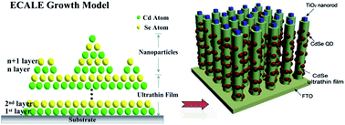
In this work, successive cadmium selenide (CdSe) ultrathin films and quantum dot layers were successfully deposited on TiO2 nanorod arrays by the electrochemical atomic layer epitaxy method (ECALE). The underpotential deposition (UPD) processes of the successive CdSe films and quantum dot layers were recorded in detail. The photo-electrochemical properties of the CdSe coated TiO2 nanorod array electrodes were also investigated, and the maximum current density reached 14.6 mA cm−2 under one sun (AM 1.5G, 100 mW cm−2). Using the ECALE method to grow a buffer layer between quantum dots and their supporting material will be useful for other energy-providing materials.
1. Introduction
Ordered nanostructures of TiO2 used as energy conversion materials have been widely studied for the last several dozen years.1–7 However, the wide band gap (3.2 eV) of TiO2 only absorbs the ultraviolet light of the sun. In order to absorb a greater part of the available sunlight, TiO2 is usually sensitized by dyes or quantum dots. In particular, quantum dots have some special properties, such as the quantum size effect,8,9 high extinction coefficients,10 large molecular dipoles, multiple charge carrier generation with a single photon11 etc., which make it possible to boost the power conversion efficiency beyond the theoretical limit of 32%.12 But the energy conversion efficiency of ∼6.5% in quantum dot sensitized solar cells is still far below that of dye-sensitized solar cells.13 This can probably be attributed to the inherent loss of electron transport with electron hopping and the recombination of active electron–hole pairs. Lots of previous research has showed that fabricating a high coverage quantum dot with an ideal size distribution, or introducing passivation films, will be able to increase the carrier charge transfer efficiency and prevent the recombination of active electron–hole pairs or trapped-stated termination.5,8,14 Recently, many methods have been used to load quantum dots on nanostructures of TiO2, such as the chemical bath deposition method,15 the successive ionic layer adsorption and reaction method,16 the direct absorption and electrodeposition method,17 the self-assembly monolayer or linker-assisted between TiO2 and quantum dots etc.8 Despite the development of various sensitization methods, the sensitizers still suffer from poor thickness and uniformity control, especially when depositing quantum dots on a high aspect-ratio TiO2 nanorod. Conventional deposition techniques usually lead to the aggregation of quantum dots. Up until now, it has remained a challenge to get a quantum dot layer on TiO2 which has high coverage and is size controllable at the same time.
The electrochemical atomic layer epitaxy (ECALE) method is a thin film deposition technique that is based on self-limiting surface reactions, by the sequential exposure of the substrate with the function of underpotential deposition (UPD) of individual elements. ECALE provides precise thickness control at the angstrom or monolayer level and allows deposition on high aspect ratio nanostructures with an excellent step coverage.18,19 By using ECALE for quantum dot deposition, the deposition process can be easily stopped by adjusting the UPD range. The size of the quantum dots could also be varied simply by tuning the number of deposition cycles, due to its excellent infiltration and conformity.20,21 ECALE has already been applied to the growth of various compound semiconductors on metal substrates, such as CdSxSe1−x,22 CdSe,23 CdTe,24 Bi2Te3,25 Sb2Te3,26 Bi2Se3.27 Here, successive CdSe thin film and quantum dot layer coated TiO2 nanorod array photoanodes are firstly fabricated by ECALE. Their possible underpotential growth mechanism and photo-electrochemical performance are then discussed in detail.
2. Experimental procedure
2.1 The growth of TiO2 nanorod arrays on the FTO substrate28
TiO2 nanorods array films were prepared by a hydrothermal growth process as follows: a certain volume of a mixture of deionised water, concentrated hydrochloric acid and titanium butoxide (97% Sigma-Aldrich) (in a 30
:
30
:
1 ratio) was firstly prepared in a Teflon-lined stainless steel autoclave (100 mL). Then, two pieces of cleaned FTO with the conductive side face up (F: SnO2, Tec 15, 10 Ω per square, Asahi) were placed at the bottom of the Teflon-liner to grow at 150 °C for 16 hours. Finally, the samples were annealed at 450 °C for half an hour in air.
2.2 The deposition of CdSe film and quantum dots on TiO2 nanorods array by ECALE
CdSe was deposited on the TiO2 nanorod arrays by ECALE at room temperature. The optimized underpotentials of Se and Cd were investigated firstly by cyclic voltammetry method on a potentiostat (Ch Instruments, CHI604D). A TiO2 nanorod array film work electrode, a Pt foil auxiliary electrode and an Ag/AgCl (3.0 M NaCl) reference electrode were employed in the three-electrode system. 5.0 mM Na2SeO3 (99%, Sigma-Aldrich) aqueous solution (pH ∼ 5.0) and 10.0 mM CdSO4 (ACS reagent 99% Sigma-Aldrich)–0.15 M EDTA2− (pH ∼ 8.5) were the deposition solutions. The pH value of the solutions was adjusted with perchloric acid and ammonia.
This underpotential deposition experiment was carried out in a computer controlled electrochemical three-electrode cell (consisting of pumps, valves, a flow cell and a potentiostat), which could auto-deliver the Na2SeO3 and CdSO4 solution and change their deposition potential synchronously by a square-wave method. The deposition procedure of CdSe was presented as follows: CdSO4 solution was firstly flushed into the electrodeposition cell to wash the film without potential for 20 s, and the chosen Cd deposition potential was kept for another 15 s; then, free solution (deionised water) was flushed through the cell for 25 s to clean the Cd2+ ions. Na2SeO3 solution was continuously flushed into the cell with the same procedure as above and the underpotential of Se was kept for 15 s. This cycle was repeated many times for each experiment. Finally, the samples were annealed at 400 °C for an hour in N2 atmosphere.
2.3 Materials characterization
The X-ray diffraction (XRD) patterns of the as-prepared films were recorded in a Philip X'pert X-ray diffractometer (Cu Kα irradiation, λ = 0.15418 nm) from 10° to 80°. Morphologies and structure information were elucidated with a Sirion 200 field emission scanning electron microscope (FE-SEM) and a FEI Tecnai G230 transmission electron microscope (TEM). A PerkinElmer Lambda 35 spectrometer UV-vis system was also used to obtain the absorption spectra of the samples.
2.4 Electrochemical measurements
The photo-electrochemical performance of the CdSe coated TiO2 nanorod array photoanodes was measured in a photo-electrochemical (PEC) cell with a auxiliary electrode of Pt foil and an Ag/AgCl reference electrode. The measurements were done in 1.0 M Na2S electrolyte solution for CdSe to maintain the stability of the electrodes.29 CHI604D was used to record the photocurrent. The photocurrent density–voltage (J–V) scan was performed from −1.2 to 0 V (versus Ag/AgCl) with a scan rate of 10 mV s−1 under an illumination intensity of 100 mW cm−2 (AM 1.5G, CHF-XM500, Trusttech). The photoconversion efficiency (η) of light to chemical energy was calculated using the following expression:30,31 |
η (%) = jp[(Erev − Eapp)/IO] × 100
| (1) |
where Erev is equal to 1.23 V (which is the potential corresponding to the Gibbs free energy change per photon in the water splitting reaction); Eapp = Emeas − Eaoc, where Emeas is the electrode potential (vs. Ag/AgCl) of the working electrode and Eaoc is the electrode potential (vs. Ag/AgCl) of the same working electrode at open-circuit conditions under the same illumination and in the same electrolyte solution; jp is the photocurrent density, and IO is the incident light intensity.
3. Results and discussion
The deposition potential was kept at an appropriate value in the underpotential region, and Cd and Se could be deposited successfully layer by layer. In order to ensure the underpotential of Cd and Se on the TiO2 electrode, the cyclic voltammograms of TiO2 electrodes were measured in Cd and Se solutions, respectively. The potentials were initially scanned in the negative direction, and reversed at different potentials. As shown in Fig. 1a, a large current was labeled as C1 at E < −0.2 V due to the reduction of Cd2+ ions. As the scanning continued, another larger current was generated due to the reductive deposition of the bulk Cd, which was labeled as C2 at −0.85 V. The subsequent anodic stripping peaks were labeled as A1 at −0.70 V and A2 at −0.38 V, respectively. The peak A2 corresponded to the bulk Cd stripping and A1 was the stripping peak of the Cd UPD layer,25 which indicates that a Cd UPD layer will be formed on the TiO2 when the underpotential is set between −0.76 and −0.38 V. A similar behavior was also observed in the deposition of Pb and Zn on Ag (ref. 22) and Cd on TiO2 nanotube film on Ti substrate in our previous work.21
 |
| Fig. 1 Cyclic voltammograms of (a) pure TiO2 nanorod electrodes recorded at 50 mV s−1 in a solution containing 10.0 mM CdSO4 and 0.15 M EDTA (pH = 8.5) and (b) TiO2 nanorod electrodes coated with a monolayer of Cd in a solution containing 5.0 mM Na2SeO3 and 0.15 M EDTA (pH = 5.0). | |
In addition, the cyclic voltammogram of the Cd-covered TiO2 surface in Na2SeO3 solution was also scanned, and is shown in Fig. 1b. Two large current peaks were respectively labeled as C3 and C4 at near −0.45 and −0.95 V, and corresponded to the underpotential and bulk deposition of Se4+ ions, which was similar to Yang's report about Bi2Se3 deposited on a Pt substrate by ECALE.27 It is reasonable to assume that the stripping of bulk Cd was not complete and showed similar characteristics to a metal substrate. In general, the underpotential of the electrode exposed to a selenium solution was around −0.45 V. Hence, the underpotential depositions of Se and Cd elements were controlled at −0.45 V and −0.65 V, respectively.
Scanning electron microscope (SEM) images of TiO2 nanorod arrays on FTO substrate before and after CdSe deposition are displayed in Fig. 2. As the comparison pictures in Fig. 2a and b show, the surface of TiO2 was gradually changed from smooth to rough (inset of Fig. 2b). The cross-section SEM images in Fig. 2c and d also show that the TiO2 nanorods were fully coated by uniform particles in a vertical direction.
 |
| Fig. 2 (a) and (b) SEM images of TiO2 nanorods before and after CdSe was deposited for 3 hours by ECALE, respectively. The inset is the local magnifying image of (b). (c) and (d) Cross-sectional SEM images of (a) and (b), respectively. | |
In order to obtain good crystallinity samples, the as-deposited TiO2 nanorod array was annealed at 400 °C for an hour in a nitrogen atmosphere. All the diffraction peaks displayed in the XRD patterns of the as-annealed sample in Fig. 3a agree with the tetragonal rutile phase of TiO2 (JCPDS no. 21-1276, a = b = 0.4582 nm and c = 0.2953 nm) and the hexagonal phase of CdSe (JCPDS no. 08-0459, a = b = 0.4299 and c = 0.7010 nm) very well. In addition, energy dispersive X-ray spectroscopy was also used to confirm whether the atomic proportion of CdSe was close to the standard chemical structure after layer by layer deposition. The data of CdSe/TiO2 in Fig. 3b show that the ratio of Cd to Se (Cd, 2.33%; Se, 2.50%) is an approximate 1
:
1 stoichiometric ratio, as expected from the formula of the CdSe compound.
 |
| Fig. 3 (a) XRD patterns of the CdSe (JCPDS no. 08-0459) coated TiO2 nanorods (JCPDS no. 21-1276). (b) EDX spectrum of the CdSe coated TiO2 electrode. | |
Transmission electron microscopy (TEM) was carried out to investigate the growth process of the CdSe. TEM images confirmed that the TiO2 nanorods were covered by uniform CdSe particles, as shown in Fig. 4a, while in high resolution images, an ultrathin film with ∼10 nm thickness was observed between the TiO2 nanorods and the CdSe particles in Fig. 4b. This agreed with our previous research on CdS thin film coating TiO2 nanotube arrays on Ti metal substrates.21
 |
| Fig. 4 (a) TEM image of a TiO2 nanorod coated with CdSe quantum dots. (b) High magnification TEM image of the CdSe/TiO2 composite. (c) SAED pattern of the ultrathin CdSe film. (d) Model of the CdSe formation processing. (e) 3D model of CdSe quantum dot and ultrathin film coated TiO2 nanorod arrays. | |
This thin film firstly formed during the underpotential deposition process due to its epitaxy mechanism. Moreover, the critical thickness of the thin film was determined by a coincidence of the strain energy density and the energy density associated with the dislocation-generating mechanism which is of minimum energy. The detailed calculation of CdSe ultrathin film thickness hc by Matthews and Blakeslee's equation is as follows:32
|
 | (2) |
The coefficient
B is the Burgers vector,
ε is the average lattice misfit (
ε ∼ 0.04824), and
ν is Poisson's ratio for CdSe (
ν ∼ 0.3512). The CdSe unit cell parameters (
a =
b = 0.4299 and
c = 0.7010 nm) were respectively introduced in
eqn (3)–(5), and results are shown as follows:
|
 | (3) |
|
 | (4) |
|
 | (5) |
Then, these results were introduced into (2), showing that the thickness of the ultrathin film is around 10 nm, where the calculated result agrees with observation. In addition, the SAED pattern of the CdSe ultrathin film was also given out in Fig. 4c. The thin film is crystalline, and the lattice planes can be indexed into (011) and (111) of the hexagonal CdSe. On the basis of the investigations into the morphology of the system described above, the formation of this interlayer could probably be attributed to the layer-by-layer growth mechanism, as follows: firstly, in the initial stage of deposition, Cd and Se atoms were deposited layer by layer and formed the ultrathin epitaxial film, until it reached the thickness limit. Then with the increase of layers, unordered atom packing formed nanoparticles, due to the unbalanced inter-atomic forces between the Cd and Se atom layers. Finally, the possible formation process and 3D model of the CdSe ultrathin film and quantum dots on TiO2 nanorods array film are shown in Fig. 4d and e, respectively.
The UV-vis absorption spectra of CdSe sensitized TiO2 electrodes are shown in Fig. 5. The absorption onset position of the bare TiO2 nanorod film was mainly located at 400 nm, which then was covered with CdSe; the absorption range red-shift to 650 nm is shown in Fig. 5a–e. It is ascribed to the quantum size effects of CdSe that the different sizes of CdSe with different deposition times helped to tune the band gap of the composite. SEM images of CdSe deposited on TiO2 nanorods film for one, two, and four hours respectively are shown in Fig. 6. Actually, the size of the CdSe quantum dots proved to be directly proportional to the deposition time, indicating that the size of the CdSe quantum dots could be controlled by adjusting the deposition time.
 |
| Fig. 5 UV-vis absorption spectra of TiO2 nanorods covered with CdSe. The deposition time of the CdSe is set from 0 to 4 hours. | |
 |
| Fig. 6 SEM images of the TiO2 nanorods after CdSe underpotential deposition for different times. (a) 1 h, (b) 2 h, (c) 4 h. | |
The photo-electrochemical conversion properties of the annealed CdSe sensitized TiO2 array photo-electrodes, with different deposition times, were characterized as shown in Fig. 7. The naked TiO2 electrode showed the lowest current density (Jsc) of around 1.8 mA cm−2, but after the decoration with the CdSe layer, the Jsc of the CdSe/TiO2 electrode increased remarkably to 14.6 mA cm−2, with a corresponding conversion η of 4.08% under one sun illumination (100 mW cm−2). The detailed open circuit potential (VOC), short circuit current (ISC), fill factor (FF), and total energy conversion efficiency (η) corresponding to these cells are also presented in Table 1. However, with a continuous increase of deposition time, the current density was significantly decreased rather than continuing to increase. For example, the current density for four hours' deposition was lower than that for 3 hours' deposition. It is reasonable to say that a lower coverage for a too-short CdSe deposition time only can absorb less light. On the contrary, an excess deposition of CdSe on the TiO2 nanorods can be generated for over-long deposition times, with the over-thick CdSe coating causing a longer transport path length for the photo-generated electron–hole pairs; this is a potential barrier for charge transfer. Then, the direct contact between the TiO2 nanorod and the electrolyte can enhance the recombination rate and generation of electron–hole pairs and lead to the electronic transmission efficiency decreasing.36 Finally, the transparent FTO substrate not only allows more light to pass and induces more CdSe quantum dots to generate photoelectrons, but it also collects the photo generated electrons from the CdSe quantum dots efficiently. The effect of an ultrathin CdSe film as the buffer layer on the electron–hole physical transfer mechanism will be investigated in detail in the near future. As a result, the improvement of the electron–hole separation and transportation environment finally leads to a stronger photocurrent intensity.
 |
| Fig. 7 (a) I–V curves of the CdSe sensitized TiO2 photo-electrodes with different deposition times. The photoelectrodes were annealed at 400 °C for an hour and then measured versus Ag/AgCl under simulated sunlight with an illumination intensity of 100 mW cm−2 in 1.0 M Na2S aqueous solution. | |
Table 1 Photovoltaic parameters of the CdSe sensitized TiO2 based QDSSCs under AM 1.5 sunlight illumination (100 mW cm−2)33–35
Samples |
Jsc (mA cm−2) |
Eapp |
FF |
η (%) |
0 (h) |
1.8 |
0.72 |
0.28 |
0.92 |
1 (h) |
5.1 |
0.89 |
0.39 |
1.73 |
2 (h) |
11.6 |
0.92 |
0.46 |
3.60 |
3 (h) |
14.6 |
0.95 |
0.58 |
4.08 |
4 (h) |
9.8 |
0.93 |
0.35 |
2.94 |
4. Conclusions
In summary, the ECALE method was used to grow successive CdSe ultrathin film and quantum dot layers on TiO2 nanorod array electrodes. The compact CdSe ultrathin film between the quantum dots and the TiO2 could prevent the direct connection of TiO2 and the electrolyte, due to its special epitaxy mechanism. The performance of the CdSe coated TiO2 electrode was also tested, and a maximum photo-electrochemical conversion efficiency (η) of 4.08% was achieved. It is possible that fabricating an ultrathin film between quantum dots and their supporting materials can significantly enhance the photovoltaic performance of quantum dot sensitized solar cells, through the ECALE method.
Acknowledgements
The authors acknowledge financial support from the National Natural Science Foundation of China (Grant no. 50827204 and 51072062), the Research Fund for the Doctoral Program of Higher Education (no. 20100142110016), the Fundamental Research Funds for the Central Universities (2010ZD014), the Cultivation Fund of the Key Scientific and Technical Innovation Project, Ministry of Education of China (no. 707044) and Nanyang Technological University (NRF CREATE program, Nanomaterials for Energy and Water Management, Singapore).
Notes and references
- S. Ruhle, M. Shalom and A. Zaban, ChemPhysChem, 2010, 11, 2290–2304 CrossRef PubMed.
- M. Graetzel, R. A. J. Janssen, D. B. Mitzi and E. H. Sargent, Nature, 2012, 488, 304–312 CrossRef CAS PubMed.
- P. V. Kamat, K. Tvrdy, D. R. Baker and J. G. Radich, Chem. Rev., 2010, 110, 6664–6688 CrossRef CAS PubMed.
- L. Etgar, W. Zhang, S. Gabriel, S. G. Hickey, M. K. Nazeeruddin, A. Eychmüller, B. Liu and M. Grätzel, Adv. Mater., 2012, 24, 2202–2206 CrossRef CAS PubMed.
-
(a) J. H. Bang and P. V. Kamat, Adv. Funct. Mater., 2010, 20, 1970 CrossRef CAS;
(b) Z. Tachan, I. Hod, M. Shalom, L. Grinis and A. Zaban, Phys. Chem. Chem. Phys., 2013, 15, 3841–3845 RSC.
-
(a) P. Roy, S. Berger and P. Schmuki, Angew. Chem., Int. Ed., 2011, 50, 2904–2939 CrossRef CAS PubMed;
(b) C. T. Yip, H. Huang, L. Zhou, K. Xie, Y. Wang, T. Feng, J. Li and W. Y. Tam, Adv. Mater., 2011, 23, 5624–5628 CrossRef CAS PubMed.
- M. Li, Y. Liu, H. Wang, H. Shen, W. Zhao, H. Huang and C. Liang, J. Appl. Phys., 2010, 108, 094304 CrossRef PubMed.
- J. Chen, W. Lei and W. Q. Deng, Nanoscale, 2011, 3, 674–677 RSC.
- W. W. Yu, L. Qu, W. Guo and X. Peng, Chem. Mater., 2003, 15, 2854–2860 CrossRef CAS.
- I. Moreels, K. Lambert, D. De Muynck, F. Vanhaecke, D. Poelman, J. C. Martins, G. Allan and Z. Hens, Chem. Mater., 2007, 19, 6101–6106 CrossRef CAS.
- R. D. Schaller and V. I. Klimov, Phys. Rev. Lett., 2004, 92, 186601 CrossRef CAS.
- W. Shockley and H. J. Queisser, J. Appl. Phys., 1961, 32, 510–519 CrossRef CAS PubMed.
- J. H. Im, C. Lee, J. Lee, S. Park and N. Park, Nanoscale, 2011, 3, 4088–4093 RSC.
-
(a) A. Kongkanand, K. Tvrdy, K. Takechi, M. Kuno and P. V. Kamat, J. Am. Chem. Soc., 2008, 130, 4007–4015 CrossRef CAS PubMed;
(b) D. A. R. Barkhouse, R. Debnath, I. J. Kramer, D. Zhitomirsky, A. G. Pattantyus-Abraham, L. Levina, L. Etgar, M. Grätzel and E. H. Sargent, Adv. Mater., 2011, 23, 3134–3138 CrossRef CAS PubMed.
-
(a) S.-C. Lin, Y.-L. Lee, C.-H. Chang, Y.-J. Shen and Y.-M. Yang, Appl. Phys. Lett., 2007, 90, 143517 CrossRef PubMed;
(b) S. Gorer and G. Hodes, J. Phys. Chem., 1994, 98, 5338–5346 CrossRef CAS.
- H. J. Lee, J. Bang, J. Park, S. Kim and S.-M. Park, Chem. Mater., 2010, 22, 5636–5643 CrossRef CAS.
- X.-Y. Yu, J.-Y. Liao, K.-Q. Qiu, D.-B. Kuang and C.-Y. Su, ACS Nano, 2011, 5, 9494–9500 CrossRef CAS PubMed.
- T. P. Brennan, P. Ardalan, H.-B.-R. Lee, J. R. Bakke, I.-K. Ding, M. D. McGehee and S. F. Bent, Adv. Energy Mater., 2011, 1, 1169–1175 CrossRef CAS.
- W. Gregory and J. L. Stickney, J. Electroanal. Chem., 1991, 300, 543–561 CrossRef.
- V. C. Fernandes, E. Salvietti, F. Loglio, E. Lastraioli, M. Innocenti, L. H. Mascaro and M. L. Foresti, J. Appl. Electrochem., 2009, 39, 2191–2196 CrossRef CAS PubMed.
-
(a) W. Zhu, X. Liu, H. Q. Liu, D. L. Tong, J. Y. Yang and J. Y. Peng, J. Am. Chem. Soc., 2010, 132, 12619–12626 CrossRef CAS PubMed;
(b) S. Feng, J. Yang, M. Liu, H. Zhu, J. Zhang, G. Li, J. Peng and Q. Liu, Electrochim. Acta, 2012, 83, 321–326 CrossRef CAS PubMed.
- M. L. Foresti, S. Milani, F. Loglio, M. Innocenti, G. Pezzatini and S. Cattarin, Langmuir, 2005, 21, 6900–6907 CrossRef CAS PubMed.
- F. Loglio, M. Innocenti, F. D'Acapito, R. Felici, G. Pezzatini, E. Salvietti and M. L. Foresti, J. Electroanal. Chem., 2005, 575, 161–167 CrossRef CAS PubMed.
- F. Forni, M. Innocenti, G. Pezzatini and M. L. Foresti, Electrochim. Acta, 2000, 45, 3225–3231 CrossRef CAS.
- J. Y. Yang, W. Zhu, X. H. Gao, S. Q. Bao, X. Fan, X. K. Duan and J. Hou, J. Phys. Chem. B, 2006, 110, 4599–4604 CrossRef CAS PubMed.
- J. Y. Yang, W. Zhu, X. H. Gao, X. A. Fan, S. Q. Bao and X. K. Duan, Electrochim. Acta, 2007, 52, 3035–3039 CrossRef CAS PubMed.
- J. Xiao, J. Y. Yang, W. Zhu, J. Y. Peng and J. S. Zhang, Electrochim. Acta, 2009, 54, 6821–6826 CrossRef PubMed.
- B. Liu and E. S. Aydil, J. Am. Chem. Soc., 2009, 131, 3985–3990 CrossRef CAS PubMed.
- M. Grätzel, J. Photochem. Photobiol., C, 2003, 4, 145–153 CrossRef.
- Z. Zhang and M. Lagally, Phys. Rev. Lett., 1994, 72, 693 CrossRef CAS.
- R. Wilby and D. Vvedensky, Phys. Rev. B: Condens. Matter Mater. Phys., 1993, 47, 4119–4122 CrossRef.
- J. W. Matthews and A. E. Blakeslee, J. Cryst. Growth, 1971, 27, 118 Search PubMed.
- E. J. Luber and J. M. Buriak, ACS Nano, 2013, 7(6), 4708–4714 CrossRef CAS PubMed.
- G. P. Smestad, F. C. Krebs, C. M. Lampert, C. G. Granqvist and H. Takakura, Sol. Energy Mater. Sol. Cells, 2008, 92, 371–373 CrossRef CAS PubMed.
- J. Yu, J. Fan and B. Cheng, J. Power Sources, 2011, 196, 7891–7898 CrossRef CAS PubMed.
- J. Fan, S. W. Liu and J. G. Yu, J. Mater. Chem., 2012, 22, 17027–17036 RSC.
|
This journal is © The Royal Society of Chemistry 2014 |
Click here to see how this site uses Cookies. View our privacy policy here.