Determination of conduction and valence band electronic structure of La2Ti2O7 thin film

Jakub Szlachetkoab, Markus Pichlera, Daniele Pergolesia, Jacinto Sá*a and Thomas Lipperta
aPaul Scherrer Institut, 5232 Villigen PSI, Switzerland. E-mail: jacinto.sa@psi.ch
bInstitute of Physics, Jan Kochanowski University, P-25-406 Kielce, Poland

Received 6th December 2013 , Accepted 11th February 2014

First published on 12th February 2014


Abstract

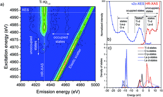
The electronic structure of a La2Ti2O7-layered perovskite thin film was determined by resonant inelastic X-ray scattering (RIXS) measurements and FEFF calculations. It was found that the empty Ti and La d-band states dominate the conduction band of the structure, whereas the top edge of the valence band is mainly composed of filled O-p states. Furthermore, there is a pronounced overlap between occupied La-p states and O-s states, which are located deeper in the valence band.


La2Ti2O7 a layered perovskite-type material has attracted interest for its piezoelectric/ferroelectric1 and photo-catalytic properties.2 Photo-catalytic water splitting is an emerging field of applied research for the production of carbon free hydrogen. TiO2 is the most studied photo-catalyst but its large band gap (∼3.0–3.2 eV) limits its application to the UV region, which only accounts for 4% of the solar spectrum. Numerous efforts have been made to decrease the TiO2 band gap, most notably doping with N, S, C3 and 3d transition metal ions.4 The enhancement in visible light absorption relates to the introduction of new in-gap electronic levels on TiO2.

Traditional characterization methods, such as diffuse reflectance spectroscopy (DRS), allow an indirect estimation of the absorption coefficient and band gap of photo-catalysts.5 Pelatt et al.6 described an empirical method to assess electronegativity, chemical hardness, and iconicity, while providing new insight into the periodic trends of solids. The technique provides a unified approach to solid state energies, solution-based reduction potentials, and several foundational concepts in chemistry and allied disciplines.

However, those techniques provide no information about the valence and conduction band electronic structure, which is essential for the rationalization of the photo-catalytic activity. Szlachetko and Sá7 used a combination of resonant inelastic X-ray scattering (RIXS) and theoretical calculations to determine the electronic structure of undoped anatase TiO2 and N-doped TiO2. This strategy allowed mapping the complete electronic structure of occupied and unoccupied states, which, in semiconductor terminology, correspond to valence and conduction band, respectively. FEFF calculations of the TiO2 density of states (DOS) revealed that the conduction band comprises the empty Ti d-band while the valence band is constituted of the occupied O p-band and Ti d-band.

In this communication, we report the maps of the electronic structure of La2Ti2O7-layered perovskite thin films, determined by using the same strategy adopted by Szlachetko and Sá in ref. 7. It was found that the empty Ti and La d-band states dominated the conduction band of the structure, whereas the valence band top edge was mainly composed of filled O-2p states.

Experimental

The La2Ti2O7 thin film was prepared by pulsed laser deposition (PLD) using a KrF excimer laser with a wavelength of 248 nm (Lambda Physik LPX300). The energy density of the laser was about 2 J cm−2 at a repetition rate of 10 Hz. The deposition was performed in a background pressure of 0.05 mbar. A sintered pellet of La2Ti2O7 prepared in our laboratory was used as target for the PLD process. The target to substrate distance was set at 5 cm. The temperature of the heater was set at 600 °C. Commercially available (110)-oriented single crystalline wafers (Crystec GmbH) of YAlO3 were used as deposition substrates. The substrates were cleaned in DI water, acetone and isopropanol in ultrasonic bath before loading into the vacuum chamber. With the selected deposition parameter, a film thickness of about 180 nm, as revealed by surface profilometry, was obtained with 30 min ablation time at 10 Hz.

The RIXS maps were collected by scanning with 0.5 eV steps around the absorption edge, and recording at each incident energy the emission spectrum with eV resolution using a wavelength dispersive spectrometer operated in the von Hamos geometry.8 The complete electronic structure of the film was determined by measuring simultaneously the Kβ and valence-to-core transitions around the Ti K-edge. We used a Ge (400) crystal in the von Hamos spectrometer, which provides a relative experimental resolution of 2 × 10⁻⁴. RIXS maps were compared to the theoretical results calculated using the FEFF9.0 code.9 The code enabled us to retrieve the orbital constitution of the La2Ti2O7 valence and conduction bands.

Results and discussion

The film diffraction pattern was found coherent with La2Ti2O7 crystal structure. Chemical analysis revealed a slightly smaller concentration of Ti and O compared to stoichiometry (ca. 1% less), believed to be due to surface termination.

The measured Kβ and v2c (valence-to-core) RIXS planes for La2Ti2O7 are plotted in Fig. 1a. For excitation energies above 4980 eV, the RIXS plane consists of the Kβ main emission line resulting from the 3p → 1s transition at emission energy around 4931 eV. The diagonal spectral feature crossing the RIXS plane at equal incoming and emitted X-ray energies relates to the elastically scattered X-rays in the sample. Since the experiments were performed using a dispersive von Hamos spectrometer, which has no moving optical components, the XES (X-ray emission spectroscopy) spectra are measured at once on a shot-to-shot basis, and the elastically scattered X-rays allow calibration of the RIXS plane with a precision of about 100 meV. Before starting the discussion of the RIXS map, we would like to emphasize that the experiments were carried out in grazing incidence geometry, which circumvents the problem of sample concentration caused by thin films, i.e., grazing incident geometry equals ‘infinitively’ thick sample.


image file: c3ra47357k-f1.tif
Fig. 1 (a) RIXS map of La2Ti2O7; (b) extracted spectra of HR-XAS (red) and valence-to-core XES (blue); (c) FEFF calculated orbital contribution.

There are several parameters that can be extracted from the RIXS plane. It should be mentioned that the presented RIXS experiments relate to the p-projected density of states (DOS) of the Ti-sites around the Fermi level. Firstly, one can determine the occupied electronic states (valence band) from the non-resonant XES spectrum (valence-to-core XES (v2c-XES)), shown in Fig. 1b. Two peaks located at 4945 eV and 4960 eV dominate the v2c-XES spectrum. The spectral features can be interpreted based on DOS calculations with the FEFF9.0 code9 (Fig. 1c). In order to compare the measured v2c structures with calculations, the XES and HR-Has spectra were scaled down in energy by a value of 4963 eV. The latter was determined from the position of the high-energy side of the v2c structure (half width) and is assigned as the Fermi energy (highest occupied electronic orbitals). The v2c-XES peak lying just below the Fermi energy (−3 eV) consists mostly of Ti-d and O-p orbitals, with a small contribution from La-p orbitals. The upper level of the valence band is primarily the O-p orbitals, similar to TiO2.7 The v2c-XES peak at −16 eV is composed of O-s and La-p orbitals. There is a very good overlap between the O-s and La-p orbitals, which explains the pronounced peak detected experimentally, contrary to what was observed with TiO2 (ref. 7) where only a weak feature related to the O-s states could be detected.

The second parameter that can be extracted is the material's unoccupied electronic states (conduction band) from the HR-XAS (high-resolution X-ray absorption spectroscopy) spectrum. HR-XAS relates to the cut across the maximum of the Kβ X-ray emission where the spectral features were assigned based on DOS calculations with the FEFF9.0 code.9 The two peaks detected on HR-XAS are associated to the Ti d-orbitals (at energies of around +4 eV and +8 eV), which are split by ca. +4 eV according to the crystal field into t2g (lower energy) and eg (higher energy) levels,10 similar to TiO2,11 and by a broad contribution from the La-d orbitals. FEFF calculations were performed using the crystal structure of La2Ti2O7, and a total of 100 atoms.

The measured occupied (red) and unoccupied (blue) p-projected DOS profiles are separated by ca. 2.8–4 eV, which encompasses the La2Ti2O7 band-gap energy.12 The result implies that the RIXS experiment provides band gap-like information, which can be used to evaluate changes to the band gap induced for example by doping. However, it should be mentioned that the band gap values estimated with this method are slightly different from the ones obtained by optical spectroscopy due to the electron–electron interaction between the 1s-excited and valence decaying electrons as well as due to core-hole screening effects. Nevertheless, the dependence on band gap narrowing or broadening by means of v2c-RIXS should be easy and straightforward detectable.

Conclusion

In conclusion, the presented method enabled the determination of La2Ti2O7 conduction and valence band orbital composition for thin films with a thickness of 180 nm. The information can be used to rationally design doped materials with enhanced visible light absorption since it is possible to determine what the orbitals contribution and the shift on the band structure edges are. The possibility to carry out the experiments in grazing incidence geometry circumvents the problem of sample concentration, often a detriment to perform high-resolution X-ray experiments with thin films. Finally, since the measurements were performed with hard X-rays, the experiments were carried out under atmospheric conditions, enabling in the future measurements to follow changes in the orbitals during water splitting under true in situ conditions.

Acknowledgements

We would like to thank the Paul Scherrer Institute for access to the SuperXAS (X10DA) beam line. The research leading to these results has received funding from the European Community's Seventh Framework Programme (FP7/2007-2013) under grant agreement no. 290605 (COFUND: PSI-FELLOW).

Notes and references

  1. (a) S. Nanamatsu, K. Kimura, K. Doi, S. Matsushita and N. Yamada, Ferroelectrics, 1974, 8, 511 CrossRef CAS; (b) S. Y. Stefanovich, S. Manamatsu and Y. N. Venevtsev, Ferroelectrics, 1980, 29, 59 CrossRef CAS; (c) W. Kinase, S. Nanamatsu, N. Ishihara, K. Hasegawa and K. Kano, Ferroelectrics, 1981, 38, 849 CrossRef CAS; (d) J. K. Yamamoto and A. S. Bhalla, J. Appl. Phys., 1991, 70, 4469 CrossRef CAS PubMed; (e) Z. M. Shao, S. Saitzek, P. Roussel, A. Ferri, O. Mentré and R. Desfeux, CrystEngComm, 2012, 14, 6524 RSC.
  2. (a) K. Onozuka, Y. Kawakami, H. Imai, T. Yokoi, T. Tatsumi and J. N. Kondo, J. Solid State Chem., 2012, 192, 87 CrossRef CAS PubMed; (b) Q. Wang, T. Hisatomi, Y. Moriya, K. Maeda and K. Domen, Catal. Sci. Technol., 2013, 3, 2098 RSC.
  3. For example: R. Asahi, T. Morikawa, T. Ohwaki, K. Aoki and Y. Taga, Science, 2001, 293, 269 CrossRef CAS PubMed.
  4. (a) O. Carp, C. L. Huisman and A. Reller, Prog. Solid State Chem., 2004, 32, 33 CrossRef CAS PubMed; (b) J. Choi, H. Park and M. R. Hoffmann, J. Phys. Chem. C, 2010, 114, 783 CrossRef CAS; (c) K. Michalow, A. Heel, A. Vital, M. Amberg, G. Fortunato, K. Kowalski, T. Graule and M. Rekas, Top. Catal., 2009, 52, 105 CrossRef; (d) K. A. Michalow, E. H. Otal, D. Burnat, G. Fortunato, H. Emerich, D. Ferri, A. Heel and T. Graule, Catal. Today, 2013, 209, 47 CrossRef CAS PubMed; (e) K. A. Michalow, D. Flak, A. Heel, M. Parlinska-Wojtan, T. Graule and M. Rekas, Environ. Sci. Pollut. Res., 2012, 10, 3696 CrossRef PubMed.
  5. (a) A. B. Murphy, Sol. Energy Mater. Sol. Cells, 2007, 91, 1326 CrossRef CAS PubMed; (b) K. A. Michalow, D. Logvinovich, A. Weidenkaff, M. Amberg, G. Fortunato, A. Heel, T. Graule and M. Rekas, Catal. Today, 2009, 144, 7 CrossRef CAS PubMed.
  6. B. D. Pelatt, R. Ravichandran, J. F. Wager and D. A. Keszler, J. Am. Chem. Soc., 2011, 133, 16852 CrossRef CAS PubMed.
  7. J. Szlachetko and J. Sá, CrystEngComm, 2013, 15, 2583 RSC.
  8. J. Szlachetko, M. Nachtegaal, E. de Boni, M. Willimann, O. V. Safonova, J. Sá, G. Smolentsev, M. Szlachetko, J. A. van Bokhoven, J.-Cl. Dousse, J. Hoszowska, Y. Kayser, P. Jagodzinski, A. Bergamaschi, B. Schmitt, C. David and A. Lücke, Rev. Sci. Instrum., 2012, 83, 103105 CrossRef CAS PubMed.
  9. (a) http://leonardo.phys.washington.edu/feff/; (b) A. L. Ankudinov, B. Ravel, J. J. Rehr and S. D. Conradson, Phys. Rev. B: Condens. Matter Mater. Phys., 1998, 58, 7565 CrossRef CAS; (c) J. J. Rehr and R. C. Albers, Rev. Mod. Phys., 2000, 72, 621 CrossRef CAS; (d) A. L. Ankudinov, J. J. Rehr, J. Low and S. R. Bare, Phys. Rev. Lett., 2001, 86, 1642 CrossRef CAS.
  10. L. K. Joseph, K. R. Dayas, S. Damodar, B. Krishnan, K. Krishnankutty, V. P. N. Nampoori and P. Radhakrishnan, Spectrochim. Acta, Part A, 2008, 71, 1281 CrossRef PubMed.
  11. L. Fleming, C. C. Fulton, G. Lucovsky, J. E. Rowe, M. D. Ulrich and J. Lüning, J. Appl. Phys., 2007, 102, 033707 CrossRef PubMed.
  12. G. Kim, D. W. Hwang, S. W. Bae, J. H. Jung and J. S. Lee, Catal. Lett., 2003, 91, 193 CrossRef.

This journal is © The Royal Society of Chemistry 2014
Click here to see how this site uses Cookies. View our privacy policy here.