Fabrication of CNx/C nanotube arrays via chemical modification in situ and application in an electronic nano-device†
Chengyong Li*abc and
Lei Heabc
aGuangdong Provincial Key Laboratory of Aquatic Product Processing and Safety, Guangdong Ocean University, Zhanjiang 524088, China. E-mail: c.y.li.ocean@gmail.com; Tel: +86-759-2396026
bKey Laboratory of Advanced Processing of Aquatic Products of Guangdong Higher Education Institution, Guangdong Ocean University, Zhanjiang 524088, China
cCollege of Food Science and Technology, Guangdong Ocean University, Zhanjiang 524088, China
First published on 23rd December 2013
Abstract
CNx/C nanotube arrays were fabricated via a simple chemical modification porous alumina membrane in situ method. The nanotubes consist of two sections featuring straight and hollow cylinder structure, one section made of N-doped carbon and the other one made of pure carbon. The metal–semiconductor junction was formed in the middle as a result of being doped or undoped with nitrogen. The on–off current ratio at ±5 V is 25. The applicability of chemical modification in situ technique provides us with a good opportunity for practical use of the multiwall nanotube for future nano-devices.
1. Introduction
The electronic properties of carbon nanotubes (CNTs) have attracted extensive interest during the last few years due to the potential applications in electronic nano-device.1–11 However, CNTs consisting of pure carbon are non-polar, which limits their applications to some extent. The presence of dopants can alter the structural and electronic properties of a nanotube dramatically.12–16 Nitrogen is probably the most common candidate used to substitute C atoms in the hexagonal graphite structures of CNTs. Previous researches have proved that doping of N atoms endowing CNTs with polar nature can have a profound influence on the electronic transport properties of CNTs.17–22 In the beginning, N-doped CNTs were fabricated by chemical vapour deposition (CVD) of N-containing organic compounds in the presence of metal nanoparticles under Argon.23–26 Although N-doped CNTs can be prepared by above method, the doping nitrogen location cannot be controlled due to the homogeneous doping environment. Kyotani et al. synthesized N-doped CNTs by template methods.27,28 Due to the restriction of nanochannels, the doping location can be controlled in the inner layer or out layer along radial direction. However, the doping nitrogen is distributed uniformly along axial direction. What new electronic properties will be observed if nitrogen doping only occurs in one section along axial direction of CNTs (CNx/C nanotubes)? Recently, diode-like rectifying characteristic was observed in a CNx/C nanotube because of its being one half doped with nitrogen.29–31 And these CNx/C nanotubes have been used to construct field-effect transistors and diode logic gate nano-devices.29 Generally, CNx/C nanotubes were fabricated via a continuous CVD two-stage process. These nanotubes consist of two segments: C nanotube segment is straight and hollow cylinder structure, while CNx nanotube segment is curved bamboo-like structure.30 Thus, there are structure defects in CNx segment, which is not beneficial to building electronic nano-device.In this manuscript, we report the first fabrication of CNx/C nanotubes via a simple chemical modifying porous alumina membrane (PAM) in situ method. Compared with bamboo-like structure CNx/C nanotubes fabricated by traditional two-stage CVD, two segments of CNx/C nanotubes have straight and hollow cylinder structure, which is important to build electronic nano-device. As shown in Scheme 1, the two segments have homogeneous structure due to the restraint from PAM nanochannels.
 | ||
| Scheme 1 Illustration of the electronic property of CNx/C nanotube arrays. | ||
Meanwhile, the electronic properties were studied and diode-like rectifying behaviour was observed. The applicability of chemical modification in situ technique provides us with a good opportunity for practical use of the CNTs for future nano-devices.
2. Experimental
The porous alumina membrane (PAM) was prepared by a two-step anodic oxidation technique (Fig. S1†).32 Before performing the two-step anodization process, a pre-anodization process is introduced to obtain relatively well aligned nanochannels. The formed concaves are used as the nucleation sites for the following classic anodization process. Dopamine self-polymerization on the PAM surface was using a procedure similar to that has been described in the literature.33 The second anodization is then performed to generate an additional porous layer below the modified porous one. Finally, free-standing PAM is formed by removing the remaining aluminium layer. CNx/C nanotubes in PAMs were fabricated via traditional CVD. Polyethylene glycol provided the main carbon source and argon flowed through the sample during the heating stage. For visualization, the as-synthesized CNTs/PAM was then dissolved in hydrofluoric acid, and the CNTs were collected by centrifugation. However, i–V tests were carried on the CNTs/PAM composite structure.3. Results and discussion
Fig. 1a–(c) show the scanning electron microscopy (SEM) images of PAM prepared at 50 V in 0.3 M oxalic acid solution. It can be estimated that the pore diameter of PAM is about 50 nm (Fig. 1a). A regular cylinder nanochannels array parallelled to each other is clearly shown (Fig. 1b) and the size is about 50 nm, which is accord with the top nanopore size. The thickness of the membrane is estimated to be 35 μm (Fig. 1c). In order to observe CNx/CNTs inside nanopores clearly, the PAM was dissolved in 5 M HF solution for 12 h at room temperature. As shown in Fig. 1d, a bundle of CNx/CNT arrays can be observed. The length of the arrays (about 35 μm, not shown) was exactly the same as the thickness of the PAM used as a template. Fig. 1e is a high magnification SEM image of CNx/CNT arrays, and the size is about 60–80 nm, which is larger than the original pore (50 nm) owing to thermal expansion of the template during growth.34 TEM image (Fig. S2†) clearly shows that CNx/C nanotubes have straight and hollow cylinder structure. | ||
| Fig. 1 SEM (a–e) and LSCM (f) images of samples. (a) Top surface of the PAM. (b) The high magnification cross-section of the PAM. (c) The whole cross-section of the PAM. (d) CNx/CNT arrays after the PAM dissolved completely. (e) The high magnification of CNx/CNT arrays. (f) LSCM (the whole cross-section) image of the PAM. | ||
Fluorescent probe fluorescein isothiocyanate (FITC) is selectively bounded to the dopamine functional layer of the PAM. A cross-sectional laser scanning confocal microscopy (LSCM) image (Fig. 1f) of the bilayered membrane clearly shows a strong green florescence of the upper layer compared to the lower layer. However, there is no significant contrast between the two layers with surface functionality from the cross-sectional SEM image (Fig. 1c). The thickness of the dopamine layer in the bilayered membrane is about 20 μm and unmodified section is about 15 μm. The length of dopamine modified or unmodified can be regulated by the anodization time. As shown in Fig. S3,† the length of modified and unmodified nanochannels is about 40 μm and 30 μm when anodization times for both steps (c) and (e) were 4 h. Thus, the lengths of CNx nanotubes and pure C nanotubes can be regulated precisely via traditional CVD due to the confined of dopamine modified PAMs.
X-ray Photoelectron Spectroscopy (XPS) characterizations in micro main were further performed to analyze the elemental composition and nitrogen bonding configurations in CNx/CNT arrays. As a matter of course, the down-section of carbon nanotube arrays without dopamine modification did not have any nitrogen (Fig. 2a), while there is an obvious N signal in the up-section of CNx/CNT arrays modified with dopamine (Fig. 2b). In addition, the signal of O 1s is appeared in two segments due to the mass of hydroxyl in dopamine and polyethylene glycol. From the area ratio of N 1s to C 1s signals corrected with standard XPS sensitivity factors, the N/C atomic ratio in N-doped CNTs is calculated to be 0.04.
 | ||
| Fig. 2 XPS spectras of different segments of CNx/CNT arrays. (a) The down-section of CNx/CNT arrays. (b) The up-section of CNx/CNT arrays. | ||
The high-resolution C 1s XPS spectra (Fig. 3a) of the as-made samples show one main peak at 284.5 eV, corresponding to sp2 hybridized graphitic carbon atoms and small signals at higher binding energy (286.5 eV) indicating some C![[double bond, length as m-dash]](https://www.rsc.org/images/entities/char_e001.gif) N and/or C–O species remaining in the samples after thermal annealing. The peaks at 287.8 eV is attributed to CO bonding configurations.35
N and/or C–O species remaining in the samples after thermal annealing. The peaks at 287.8 eV is attributed to CO bonding configurations.35
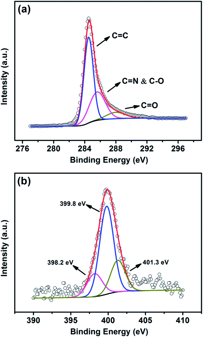 | ||
| Fig. 3 High-resolution C 1s (a) and N 1s (b) spectras of CNx/CNT arrays. | ||
Similarly, the bonding configurations of nitrogen atoms were characterized by high-resolution N 1s spectra. The N 1s XPS spectrum (Fig. 3b) is divided into three components.36 The peaks with lower binding energy located at about 398.2 and 399.8 eV, respectively, correspond to pyridine-like (17%, atom ratio) and pyrrole-like (61%, atom ratio) nitrogen, as illustrated in Fig. 4, which can contribute to the π-conjugated system with a pair of p-electrons in the graphite layers. When carbon atoms within the graphite layers are substituted by nitrogen atoms in the form of “graphitic” nitrogen, the corresponding peak in the high-resolution N 1s spectra is located at 401.3 eV (22%, atom ratio). In addition, the curve fitting suggests that the main functionality in N-doped CNTs is pyridone/pyrrole.
 | ||
| Fig. 4 A proposed structure of N-doped CNTs.37 | ||
Fig. 5 shows the i–V curves of C nanotube arrays and CNx/C nanotube arrays at room temperature. The i–V curve of C nanotube arrays is linear, while there is a distinct rectifying characteristic of CNx/C nanotube arrays. Therefore, we can conclude that the rectifying behavior of the CNx/C nanotube arrays should be attributed to nitrogen doping in one segment. Pure CNTs are metallic,3 and N-doped CNTs are n-typed tubes.38 In this condition, CNx/C nanotube constitutes a metal–semiconductor junction. The on–off current ratio at ±5 V is 25 calculated from eqn (1).
 | (1) |
 | ||
| Fig. 5 i–V curves of CNx/C nanotube arrays (a) and C nanotube arrays (b), respectively. The inset shows a logarithmic plot of the i–V characteristic. | ||
4. Conclusion
In conclusion, CNx/C nanotube arrays were fabricated via simple chemical modifying PAM in situ. Two constituting segments (CNx and C) both have homogeneous hollow cylinder structure and the lengths of each segment can be regulated precisely by controlling the relevant length of modified or unmodified nanochannels of the PAM. Electrical transport measurements indicate that there is a distinct diode-like rectifying behaviour of CNx/C nanotube arrays. The applicability of chemical modification in situ technique provides us with a good opportunity for practical use of the multiwall nanotube for future nano-devices.Acknowledgements
This work was supported by Foundation of Guangdong Ocean University (E13393).References
- W. A. deHeer, W. S. Bacsa, A. Châtelain, T. Gerfin, R. Humphrey-Baker, L. Forro and D. Ugarte, Science, 1995, 268, 845 CAS.
- C. L. Kane and E. J. Mele, Phys. Rev. Lett., 1997, 78, 1932 CrossRef CAS.
- Z. Yao, H. W. C. Postma, L. Balents and C. Dekker, Nature, 1999, 402, 273 CrossRef CAS PubMed.
- M. Ouyang, J. L. Huang and C. M. Lieber, Acc. Chem. Res., 2002, 35, 1018 CrossRef CAS PubMed.
- M. S. Strano, C. A. Dyke, M. L. Usrey, P. W. Barone, M. J. Allen, H. Shan, C. Kittrell, R. H. Hauge, J. M. Tour and R. E. Smalley, Science, 2003, 301, 1519 CrossRef CAS PubMed.
- E. Bekyarova, M. E. Itkis, N. Cabrera, B. Zhao, A. Yu, J. Gao and R. C. Haddon, J. Am. Chem. Soc., 2005, 127, 5990 CrossRef CAS PubMed.
- M. S. Arnold, A. A. Green, J. F. Hulvat, S. I. Stupp and M. C. Hersam, Nat. Nanotechnol., 2006, 1, 60 CrossRef CAS PubMed.
- V. Sgobba and D. M. Guldi, Chem. Soc. Rev., 2009, 38, 165 RSC.
- H. Klauk, Nat. Nanotechnol., 2013, 8, 158 CrossRef CAS PubMed.
- J. Waissman, M. Honig, S. Pecker, A. Benyamini, A. Hamo and S. Ilani, Nat. Nanotechnol., 2013, 8, 569 CrossRef CAS PubMed.
- Q. Cao, S. j. Han, G. S. Tulevski, Y. Zhu, D. D. Lu and W. Haensch, Nat. Nanotechnol., 2013, 8, 180 CrossRef CAS PubMed.
- C. Zhou, J. Kong, E. Yenilmez and H. Dai, Science, 2000, 290, 1552 CrossRef CAS.
- A. Javey, R. Tu, D. B. Farmer, J. Guo, R. G. Gordon and H. Dai, Nano Lett., 2005, 5, 345 CrossRef CAS PubMed.
- J. Campos-Delgado, I. O. Maciel, D. A. Cullen, D. J. Smith, A. Jorio, M. A. Pimenta, H. Terrones and M. Terrones, ACS Nano, 2010, 4, 1696 CrossRef CAS PubMed.
- A. A. Koós, F. Dillon, E. A. Obraztsova, A. Crossley and N. Grobert, Carbon, 2010, 48, 3033 CrossRef PubMed.
- H. Fang, M. Tosun, G. Seol, T. C. Chang, K. Takei, J. Guo and A. Javey, Nano Lett., 2013, 13, 1991 CrossRef CAS PubMed.
- R. Czerw, M. Terrones, J. C. Charlier, X. Blase, B. Foley, R. Kamalakaran, N. Grobert, H. Terrones, D. Tekleab, P. M. Ajayan, W. Blau, M. Rühle and D. L. Carroll, Nano Lett., 2001, 1, 457 CrossRef CAS.
- B. Wang, Y. Ma, Y. Wu, N. Li, Y. Huang and Y. Chen, Carbon, 2009, 47, 2112 CrossRef CAS PubMed.
- H. Khalfoun, P. Hermet, L. Henrard and S. Latil, Phys. Rev. B: Condens. Matter Mater. Phys., 2010, 81, 193411 CrossRef.
- P. Ayala, R. Arenal, M. Rümmeli, A. Rubio and T. Pichler, Carbon, 2010, 48, 575 CrossRef CAS PubMed.
- C. L. Pint, Z. Sun, S. Moghazy, Y. Q. Xu, J. M. Tour and R. H. Hauge, ACS Nano, 2011, 5, 6925 CrossRef CAS PubMed.
- L. Lu, T. Xu, W. Chen, J. M. Lee, Z. Luo, I. H. Jung, H. I. Park, S. O. Kim and L. Yu, Nano Lett., 2013, 13, 2365 CrossRef CAS PubMed.
- M. Terrones, P. Redlich, N. Grobert, S. Trasobares, W. K. Hsu, H. Terrones, Y. Q. Zhu, J. P. Hare, C. L. Reeves, A. K. Cheetham, M. Rühle, H. W. Kroto and D. R. M. Walton, Adv. Mater., 1999, 11, 655 CrossRef CAS.
- M. Glerup, M. Castignolles, M. Holzinger, G. Hug, A. Loiseau and P. Bernier, Chem. Commun., 2003, 2542 RSC.
- K. Ghosh, M. Kumar, T. Maruyama and Y. Ando, J. Mater. Chem., 2010, 20, 4128 RSC.
- K. S. Lee, W. J. Lee, N. G. Park, S. O. Kim and J. H. Park, Chem. Commun., 2011, 47, 4264 RSC.
- W. Xu, T. Kyotani, B. K. Pradhan, T. Nakajima and A. Tomita, Adv. Mater., 2003, 15, 1087 CrossRef CAS.
- X. Yang, A. Tomita and T. Kyotani, J. Am. Chem. Soc., 2005, 127, 8956 CrossRef PubMed.
- P. A. Hu, K. Xiao, Y. Liu, G. Yu, X. Wang, L. Fu, G. Cui and D. Zhu, Appl. Phys. Lett., 2004, 84, 4932 CrossRef CAS PubMed.
- K. Xiao, Y. Fu, Y. Q. Liu, G. Yu, J. Zhai, L. Jiang, W. P. Hu, Z. G. Shuai, Y. Luo and D. B. Zhu, Adv. Funct. Mater., 2007, 17, 2842 CrossRef CAS.
- E. Cobas and M. S. Fuhrer, Appl. Phys. Lett., 2008, 93, 043120 CrossRef PubMed.
- H. Masuda and K. Fukuda, Science, 1995, 268, 1466 CAS.
- H. Lee, S. M. Dellatore, W. M. Miller and P. B. Messersmith, Science, 2007, 318, 426 CrossRef CAS PubMed.
- J. Li, C. Papadopoulos and J. Xu, Nature, 1999, 402, 253 CAS.
- T. I. T. Okpalugo, P. Papakonstantinou, H. Murphy, J. McLaughlin and N. M. D. Brown, Carbon, 2005, 43, 153 CrossRef CAS PubMed.
- C. Morant, J. Andrey, P. Prieto, D. Mendiola, J. M. Sanz and E. Elizalde, Phys. Status Solidi A, 2006, 203, 1069 CrossRef CAS.
- D. Wei, Y. Liu, Y. Wang, H. Zhang, L. Huang and G. Yu, Nano Lett., 2009, 9, 1752 CrossRef CAS PubMed.
- R. Czerw, M. Terrones, J. C. Charlier, X. Blase, B. Foley, R. Kamalakaran, N. Grobert, H. Terrones, D. Tekleab, P. M. Ajayan, W. Blau, M. Rühle and D. L. Carroll, Nano Lett., 2001, 1, 457 CrossRef CAS.
Footnote |
| † Electronic supplementary information (ESI) available. See DOI: 10.1039/c3ra47337f |
| This journal is © The Royal Society of Chemistry 2014 |