Three-dimensional chemical sensors based on rolled-up hybrid nanomembranes†
Céline Vervacke*ab,
Carlos C. Bof Bufon*ac,
Dominic J. Thurmera and
Oliver G. Schmidtabde
aInstitute for Integrative Nanosciences, IFW Dresden Helmholtzstraße 20, 01069 Dresden, Germany. E-mail: c.vervacke@ifw-dresden.de
bCenter for Advancing Electronics Dresden, TU Dresden, Germany
cBrazilian Nanotechnology National Laboratory, CNPEM, PO Box 619, 13083-970, Campinas, SP, Brazil. E-mail: cesar.bof@lnnano.cnpem.br
dMaterial Systems for Nanoelectronics, Chemnitz University of Technology, Reichenhainer Straße 70, 09107 Chemnitz, Germany
eMerge Technologies for Multifunctional Lightweight Structures, TU Chemnitz, Germany
First published on 28th January 2014
Abstract
Moving towards the realization of ultra-compact diagnostic systems, we demonstrate the design, realization and characterization of rolled-up nanomembrane-based chemical sensing elements operating at room temperature. The tube-shaped devices with a final diameter of ∼15 μm rely on a fabrication process which combines top-down and bottom-up approaches and is compatible with standard processing technologies. Arrays of sensors are created in parallel on-a-chip, consequently, the integration of such elements into lab-in-a-tube devices as sensing units certainly seems feasible. The sensing properties of the devices are created by the selective incorporation of thin organic active layers in the inner wall of the microtubes. While the sensitivity towards volatile organic compounds is observed to be similar to previously reported sensors, indicating that the integration of the organic layer is efficiently achieved, the occupied footprint area of the tube-shaped devices is at least one order of magnitude smaller than its planar counterpart. This particular feature makes this procedure an attractive pathway to condense sensing elements for ultra-compact devices.
Introduction
The systematic demand for increased functionality in micrometer scale devices has pushed forward the development of ultra-compact diagnostic systems such as the recently introduced lab-in-a-tube concept.1 In this concept, each functional element is rolled-up into a compact component and integrated into a single tube.Self-curling of strain-engineered layers2,3 is the most elegant way to manufacture well-positioned and multi-functional tubes on a single chip in a parallel fashion.4–8 In particular, rolled-up tubes provide easy access to the tubes' inner walls allowing their functionalization towards the targeted applications.1,9,10 In this technology, pre-strained thin films are released from a host substrate by selectively removing an underlying sacrificial layer. During this process, the strain in the thin film relaxes and the layers roll up into a 3D architecture. By combining top-down and bottom-up methods, rolled-up technology allows creating a large variety of active elements4,8,11–13 and in particular tubular sensors, key elements to every laboratory. While magnetic,14–16 optical17–20 and optofluidic21–24 sensors have already been developed, there is, to the best of our knowledge, no report of an organic tubular sensor device. We fill this gap by presenting in this work an integrated and operational polypyrrole (PPy)-based organic–inorganic hybrid sensor.
PPy is a major representative of conductive polymers (CP). The interest of this material class lies in that CP-based sensors possess a high sensitivity, a low detection limit and operate at room temperature compared to traditional oxide based sensors.25 Amongst CPs, PPy is of great interest due to its easy synthesis on insulating substrates,26,27 high conductivity28,29 and good electrical stability under standard conditions.30,31 Several investigations have already been carried out to detect harmful vapours of volatile organic compounds (VOCs) with “pure” PPy32,33 and PPy-based composites,34,35 going as far as to attempt integrating these sensors to fabricate electronic noses.36,37 The major drawback of organics however is that they are fragile and easily damaged during the integration process.38
Self-curling circumvents this issue by allowing us to deposit the organic layer last on a planar system and to roll it up at ambient conditions to become the innermost shell in the 3D architecture. The end device is a hybrid system combining the robustness of an inorganic backbone with the chemical flexibility39 of organic active layers. Last but not least, the inorganic backbone permits the use of metal electrodes and makes the whole process compliant with standard on-chip technologies.
As a proof of concept, we create a large array of tube-shaped gas sensing elements on a chip for detecting VOCs vapours, like alcohols, hydrocarbons, esters and ketones, all known to be hazardous for humans.40–42 The roll-up procedure adopted gives rise to 3D devices with an occupied footprint area at least one order of magnitude smaller than their planar counterparts, a hollow volume of less than 50 pL and a sensitivity comparable to large area elements. Furthermore, this tubular shape is essential for future integration of the sensor into lab-in-a-tube systems.
Results and discussion
The use of rolled-up nanomembranes as a chemical sensing element depends on the perfect integration of two components on the inner walls of the microtubes: the electrodes that establish the electrical contact with the external world, and the active layer, which brings the desired functionality. An illustration in Fig. 1 shows the concept of a rolled-up chemical sensor (RUS). | ||
| Fig. 1 Illustration of the rolled-up sensor, highlighting the electrodes integration and the active organic layer integrated into the nanomembrane-based microtube. | ||
The addition of electrodes into the rolled-up structure is strongly related to the capability to control the strain gradients throughout the axial direction. Usually, for a continuous nanomembrane, this fundamental point is not fully considered since the driving force for the rolling is homogeneous along the axial direction.43,44 However, by patterning spaced electrodes on top of a strained layer before the rolling, changes in the strain gradients appear across the structure. It can lead to a break-up of the nanomembrane in the gap region between the electrodes during the tube formation (see ESI Fig S1†). Therefore, any attempt to integrate the electrodes into the rolled-up microtubes has first to minimize such damage.
The fabrication process developed here allows us to simultaneously address both issues; the effective patterning of the electrodes into the microtube, and the incorporation of the organic materials without losing its physical/chemical properties. The complete fabrication steps are described in detail in the schematic of Fig. 2. The hybrid RUS were fabricated on Si (100) wafers covered by 1 μm SiO2. Nevertheless, there is no technical limitation for using alternative substrates like glass or alumina plates, for instance. The whole patterning is done by conventional photolithography, making it technically viable in modest infrastructures.
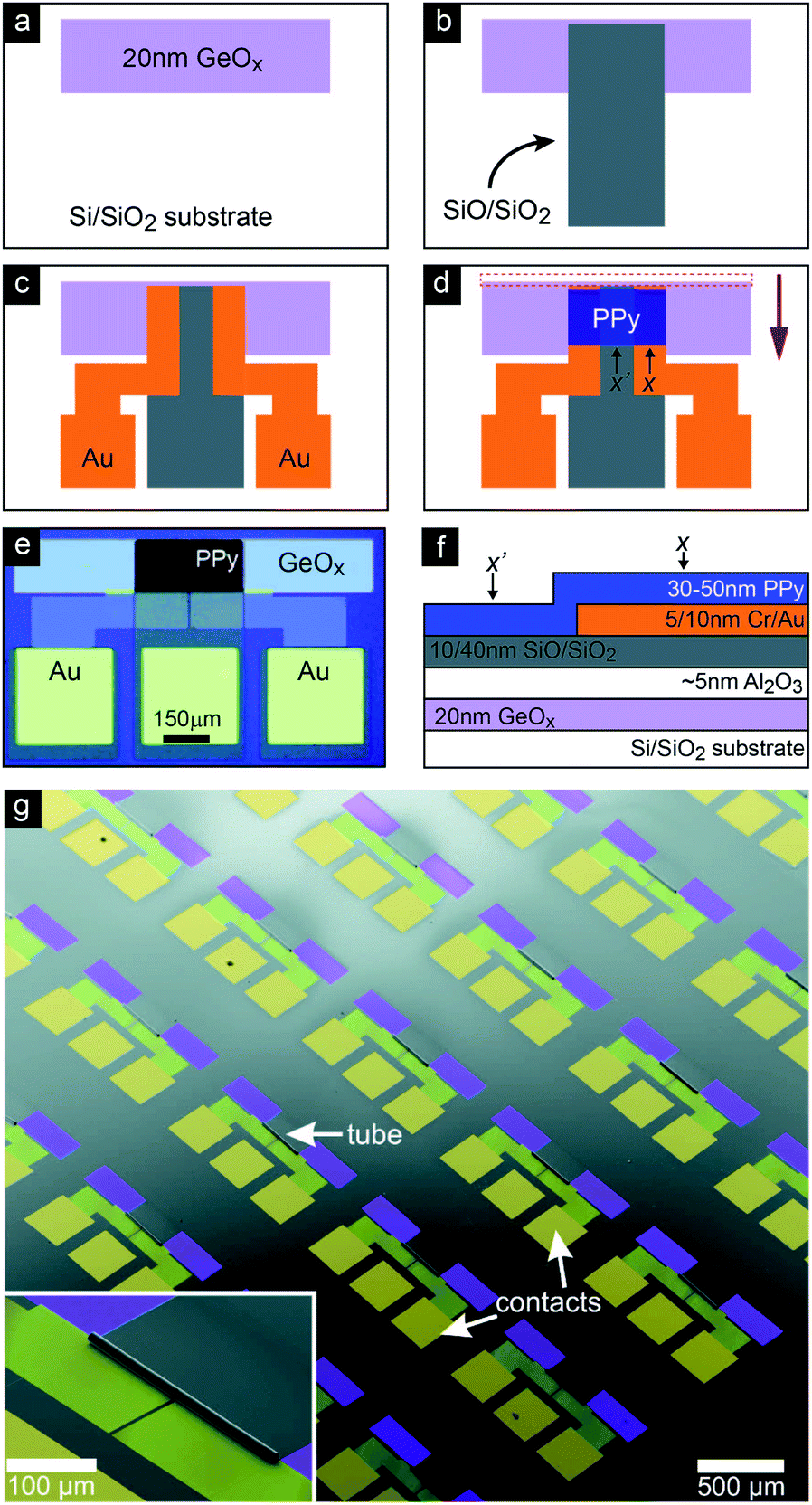 | ||
| Fig. 2 (a–d) Fabrication steps to form the RUS including the patterning of the (a) sacrificial layer, (b) strained layer, (c) contacts and (d) active organic layer. (e) Optical image of the structure prior rolling. (f) Description of the layers stack composition at two different positions (see d): at the electrodes region (X) and on the gap in-between electrodes (X′). (g) Large array of devices fabricated in parallel on-a-chip (inset: image of a single RUS). | ||
The first fabrication step, illustrated in Fig. 2a, consists of the definition of the germanium (Ge) based sacrificial layer (20 nm). After electron-beam deposition, the Ge layer is oxidized by an oxygen plasma treatment. Alternatively, the sample can be baked at 70 °C for 12 hours in air. The main advantage of this category of sacrificial layer lies in the fact that it can endure the whole fabrication process and be easily removed in water.4 Therefore, by this choice, it is possible to ensure a minimum damage to the organic layer during the formation of the RUS and to control the release of the strained layer deposited in the next fabrication step. As a result, the releasing speed can be adjusted to avoid any damage of the nanomembrane.
Next, the SiO/SiO2 (10/40 nm) strained layer is deposited by electron-beam evaporation on top of the freshly prepared GeOx layer with a deposition rate of 5 Å s−1 and 0.5 Å s−1, respectively (Fig. 2b). This layer was carefully designed to fulfill four requirements: (a) allow for roll-up of the whole system (including the electrodes and the active layer) with a minimum of damage, (b) guarantee electrical insulation between windings; (c) ensure a final tube diameter smaller than 15 μm (to permit an integration with other tube-shaped elements)45 by tuning the bilayer thicknesses, and (d) to be able to sustain the nanomembrane in a tubular shape without collapsing. The last characteristic is necessary to avoid the use of supercritical drying in the fabrication process, which may lead to the damage of the active layer.5 After the strained layer, fifty cycles of Al2O3 (∼5 nm) are deposited by atomic layer deposition (ALD). Next, the thin Au electrodes (5 nm Cr/10 nm Au) are prepared on top of the strained layer (see Fig. 2c), followed by the thermal deposition of contact pads. The strain configuration which guarantees an effective release and the roll-up of the sensor is mainly generated by tuning the thin films deposition rates and thicknesses. Therefore, a thorough investigation of the effects of each layer added to the system is of great importance. As an example, in spite of the fact that the SiO2 brings the robustness necessary to avoid any damage of the tube during rolling, this layer is observed to reduce the overall strain in the system and to suppress the rolling. On the other hand, the addition of a bimetallic layer (Cr/Au) on top of it, which also serves as electrode, tends to increase the strain gradient46 and promotes the roll-up of the nanomembrane.
Before rolling, a trench is opened across the Al2O3 layer by a five seconds HF (∼6.7% v/v) dip (red dashed line in Fig. 2d). This opening is used to allow the water to access the sacrificial layer and to induce a preferential rolling direction. The PPy active layer is chemically polymerized on top of the Au electrodes using the vapor phase of the pyrrole monomer as described elsewhere.26 The PPy film thickness was found to be between 30 and 50 nm and it is also patterned by photolithographic means. Fig. 2e shows an optical image of a device after the microfabrication process and immediately before rolling up the hybrid nanomembrane. The complete description of the layers stack composition is shown in Fig. 2f at two different positions (see Fig. 2d): at the electrodes region (X) and at the gap in-between the electrodes (X′).
By the selective removal of the GeOx layer in warm water (60 °C), the planar tail of the device, placed on top of the sacrificial layer, rolls up into microtubes with a diameter (d) of ∼(15 ± 3) μm (up to 4 windings) in roughly one hour. This result represents a reduction of the footprint area of the sensors active region of about one order of magnitude (from 4.5 × 10⁻² to 4.5 × 10⁻³ mm2). Fig. 2g shows an array of RUS to highlight the parallel nature and reproducibility of the fabrication process; the fabrication yield is about 70 to 90%. After rolling, the tubes are kept in inert atmosphere prior to measurements.
In the cross-sectional images of Fig. 3, the incorporation of the PPy nanomembranes into the micrometer-tube to form a hybrid RUS is verified. The longitudinal cross-sectional image (Fig. 3a) also highlights the integrated electrodes, which are separated by a 5 μm gap, and the PPy layer in-between the electrodes. Note that the organic layer was successfully deposited on top of the insulating underlying layer (SiO/SiO2) to form the tube wall. Here it is worth to mention that by electrochemical means the PPy layer could not be grown and patterned simultaneously on an insulating surface with the thicknesses reported in this work.29,31
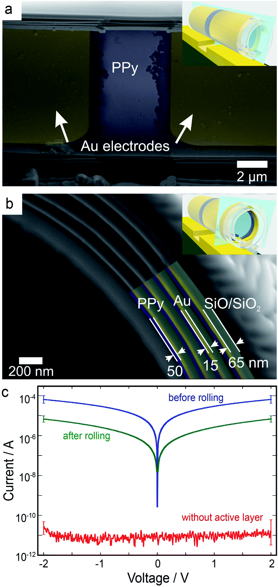 | ||
| Fig. 3 Cross-sectional image of the RUS (a) along the tube axis and (b) exhibiting the different layers integrated in the tube. (c) Current–voltage (I–V) characteristic measured without the PPy layer, before and after rolling the devices. The curves represent an average of several I–V traces obtained from different devices. | ||
As shown in Fig. 3, the thickness of the organic layer is observed thicker close to the electrodes. The whole film exhibits an egg-like structure typical for such thinness (see AFM image in Fig. S2†).26
After rolling, the tube walls form a free-standing hybrid organic–inorganic heterostructure comprising periodic layers of oxide/metal/organics or oxide/organic, depending on the section considered (Fig. 3b). On top of the electrodes (X region according to Fig. 2d), for instance, the radial hybrid heterojunction is a combination of materials out of three different classes, namely PPy/Au/SiO/SiO2. Since the tube performed about four windings, the radial heterostructure in this case comprises about three periods.
As shown at the edge of the tube image of Fig. 3a, the electrodes and the thicker PPy layer on top of them allow for the formation of voids in-between the consecutive windings in the gap region. Thus, the radial heterojunction in this region comprises three periods of vacancy/PPy/SiO/SiO2 layers. This approach for creating radial heterojunctions is an alternative option for developing hybrid systems, in both radial and longitudinal directions, by combining material of different classes and properties.47,48
By exploiting the longitudinal axis of the tube one can, for instance, create a variety of heterojunctions; each one bringing unique functionalities to the structure: from magnetic to optical responses as well as chemical and biological sensitivities. It is worth mentioning that, to the best of our knowledge, there is no method reported so far that allows either the precise integration of such a conducting polymer into confined and insulating environments, or the creation of periodic radial hybrid heterojunctions combining materials from different classes.47,48
The electrical properties of the integrated rolled-up PPy nanomembranes, or any other material eventually placed instead, are probed via the patterned electrodes that are externally connected by bonding pads. In Fig. 3c the current–voltage characteristics (I–V) of RUSs are obtained during different steps of the fabrication process for more than one hundred devices on-a-chip (see Fig. 2g). As expected, before the deposition of the active layer, the measured current is below the instruments detection limit, indicating that the gap between the electrodes is essentially open. By comparison, the PPy containing RUS exhibit a current increase of roughly six orders of magnitude at the highest applied bias. This observation not only indicates that the organic nanomembrane is successfully integrated, but also that it is connected between the electrodes. The decrease of the current observed after rolling is explained by the reduction process suffered by the PPy nanomembrane due to the partial removal of counterions during the roll-up step in water.49 Apart from the current decrease, the fabrication process allows the polymer to be confined in the tube without losing its main electrical property, namely the high conductivity.
By applying a constant bias to the external contact pads, the total current flowing across the RUS under inert gas injection (here N2) is defined by I0 = I01 + I02, where the first term (I01) is the current across the PPy layer on the inner tube wall and the second (I02), the current through the layer embedded in between windings. Since the electrodes gap separation and the film thickness are constant along the contacts extension, the fraction of current flowing across the active area in the inner surface of the tube can be written as:
 | (1) |
 | (2) |
We proceed evaluating the sensing response to the RUS against VOCs exposure. In order to compare the behavior of the RUS towards different species, we define the sensitivity as:
 | (3) |
Note that S is taking into account only the contributions of the organic thin film deposited on top of the tube inner walls.
In Fig. 4a, the RUS reproducibility towards methanol is plotted for fifteen seconds pulses of saturated methanol vapor. The methanol vapor is carried by N2. In order to clean the inner part of the tube, dry N2 is further injected for two minutes. On average, S was found around (19.3 ± 2.1)% upon the number of cycles performed. The same test was repeated for other VOCs (tetrahydrofuran (THF), acetone, ethanol and acetonitrile) and water vapor. The results are summarized in the inset table of Fig. 4a. Regardless of the injected VOC, the RUS exhibit a quick response (from 1 nA s−1 to 5 nA s−1) towards all examined species. In addition to maintain S among the best values reported in literature,50,51 the RUS tubular shape guarantees a reduction of the devices footprint area by at least one order of magnitude. Such a feature is of relevance when the integration of the sensing element into lab-in-a-tube systems is desired. A direct comparison between rolled and planar devices is not possible for as-grown active layers since during rolling the PPy layer is also partially discharged. However, the evaluation of discharged active layers does not show significant differences between planar and rolled devices. Nevertheless, this is a particular feature observed for PPy active layers and cannot be extended for other materials. As previously reported,33 the current across PPy films tends to decrease when exposed to certain organic solvents. As shown in Fig. 4b, by applying a constant bias of 100 mV, similar behavior can be observed once saturated methanol vapor is injected through the RUS: the current drops ∼7% at a rate of ∼5 nA s−1. Once the VOC injection stops and dry N2 flows across the tube, the current is recovered to its base value after ∼120 seconds. Such reversibility indicates that the original counterions embedded in the PPy during growth (Cl−) are not removed during the sensing operation,52 suggesting that the sensing mechanism under methanol as well as other VOCs exposure are in fact associated with changes in the PPy thin film volume.53,54
 | ||
| Fig. 4 (a) Sensitivity-time dependence for methanol measured at V = 0.1 V for ten pulses (15 s). The inset table shows the sensitivity of the device towards different solvents (THF (tetrahydrofuran), acetone, ethanol, acetonitrile, water vapor and methanol). (b) Current–time dependence for methanol illustrating the response and relaxation times. | ||
Once the methanol exposure stops and N2 is re-injected into the tube, the current recovering is observed to follow the stretched exponential function (also known as Kohlrausch law), given by:55
 | (4) |
From the data fitting, β was found being 0.33 ± 0.03 and agrees with the values reported for relaxation processes due to swelling and de-swelling of organic layers under humidity changes.56 By comparison to τ values reported for similarly made PPy thin films exposed to O2/N2 cycles,26 the relaxation time observed here (∼830 hours) is at least one order of magnitude smaller, while τ is very similar (0.4). The explanation for changes on the electrical properties of the PPy layers in presence of VOCs is given in terms of weak physical interactions like the hydrogen bonding to polar groups. This bonding causes deformations of the polymeric chain via adsorption or swelling.32,54 Since the conduction across PPy films strongly depends on both inter- and intra-chain charge hopping,57,58 the swelling process is expected to increase the inter-chain separation. This separation suppresses the current across it and forces the conduction through different pathways with higher resistance. By de-swelling, the chain separation decreases and the inter-chain hopping is recovered leading to a current increase. Besides the species reported above, we also tested acetic acid, diethyl ether, isopropanol and toluene. The corresponding sensitivities for these vapors were found, however, below the noise level. One possible reason for the weak response towards some chemicals is the high sensitivity of the PPy nanomembrane towards water vapor present in most of the solutions used (see table in Fig. 4a). In this case, there is a competitive adsorption between the analyte solvent molecules and the water vapor comprised in it.33 As already reported for methanol,33 a “memory-like” effect might also play a role for water, since it is the rolling media. However, such features are mainly associated with the functional layer chosen and a better selectivity could be achieve by using other material classes like oxides, self-assembled monolayers or nanoparticles. In order to compensate this deficiency, one can alternatively incorporate several functional layers along the same tube-shaped element so that a large variety of chemicals may be detected and/or quantified simultaneously on a single device. As already discussed, from the fabrication point of view, there is no limitation for either creating more complex hybrid stacking layers or multi-section arrays along the inner tube wall.
Conclusions
In conclusion, we demonstrate a novel platform to create ultra-compact sensing elements based on hybrid organic–inorganic nanomembranes which would eventually be suitable for lab-in-a-tube systems.1 For the demonstrator presented here, we were not only able to integrate metallic electrodes inside of a rolled-up microtube element, but also to selectively incorporate an organic nanomembrane (PPy) as an active layer on top of it. By using SiO/SiO2 as a strained bilayer on top of a GeOx sacrificial layer, we obtained a high yield of integrated rolled-up microelectrodes embedded on a single chip. The SiO/SiO2 strained bilayer makes the system robust, biocompatible and transparent, which is relevant for a variety of alternative applications such as cells counting.59,60 The GeOx sacrificial layer guarantees that the rolling process can occur in water making the incorporation of organic and biological systems prior to tube formation feasible. This feature represents a completely different route towards the development of functional ultra-compact devices. In order to incorporate the functionality into the rolled-up structure, we demonstrate the successful integration of a PPy nanomembrane and its contacts on the inner wall of the microtubes without compromising the device's properties.The rolled-up sensors manufactured by this approach were tested to detect volatile organic compounds. Moreover, the system is highly flexible, can operate at room temperature and may be tuned to investigate the physical/chemical properties of different active layers (for instance, molecular layers, magnetic materials and insulators), deposited on various electrode materials, in confined micro-environments.
Considering that microtube-based sensors can be used to optically evaluate and confine cells60 and liquids,59 our capability to selectively and deterministically integrate electrodes and organic materials inside such microtubes extends the potential of strained rolled-up nanomembranes and makes this technology an important platform towards ultra-compact systems and devices.
Experimental section
Device fabrication
All the patterning steps are done by optical lithography using the photoresist AZ5214E. On thermally oxidized Si(100) wafer, a germanium (Ge) based sacrificial layer (20 nm) is defined. After electron-beam deposition, the Ge layer is oxidized by an oxygen plasma treatment. Alternatively, the sample can be baked at 70 °C for 12 hours. Next, the SiO/SiO2 strained layer is deposited by electron-beam evaporation on top of the freshly prepared GeOx layer with a deposition rate of 5 Å s−1 and 0.5 Å s−1, respectively. After the strained layer, fifty cycles Al2O3 (∼5 nm) are deposited by atomic layer deposition (ALD). Next, the thin Au electrodes (5 nm Cr/10 nm Au) are prepared on top of the strained layer, followed by the thermal deposition of contact pads. Before rolling, a trench is opened across the Al2O3 layer by a five secondes HF (∼6.7% v/v) dip. The PPy active layer is chemically polymerized on top of the Au electrodes using the vapour phase of the pyrrole monomer as described elsewhere.26Sensor characterization
All the chemicals (p.a. grade) were used as purchased, without further purification. Prior to the measurements, the devices were individually bonded for connection to a Keithley 2400A. The chip was placed in a measurement chamber at room temperature and atmospheric pressure (see schematic of the setup in Fig. S3†). Current measurements were performed as a function of time on the functionalized devices at a bias of 0.1 V. Solvents vapors were obtained by bubbling nitrogen into room temperature solvents. The sensor was exposed alternatively to pure nitrogen for two minutes and to the solvent vapor for 15 seconds.Acknowledgements
M. Bendova, D. Grimm, M. Bauer and F. C. Frazatto are acknowledged for fruitful discussions and technical support. This work was partly found by the DFG Research Unit 1713.Notes and references
- E. J. Smith, W. Xi, D. Makarov, I. Mönch, S. Harazim, V. A. Bolaños Quiñones, C. K. Schmidt, Y. F. Mei, S. Sanchez and O. G. Schmidt, Lab Chip, 2012, 12, 1917–1931 RSC.
- O. G. Schmidt and K. Eberl, Nature, 2001, 410, 168 CrossRef CAS PubMed.
- V. Y. Prinz, V. A. Seleznev, A. K. Gutakovsky, A. V. Chehovskiy, V. V. Preobrazhenskii, M. A. Putyato and T. A. Gavrilova, Phys. E, 2000, 6, 828–831 CrossRef CAS.
- C. C. Bof Bufon, J. D. Cojal González, D. J. Thurmer, D. Grimm, M. Bauer and O. G. Schmidt, Nano Lett., 2010, 10, 2506–2510 CrossRef CAS PubMed.
- Y. F. Mei, A. A. Solovev, S. Sanchez and O. G. Schmidt, Chem. Soc. Rev., 2011, 40, 2109–2119 RSC.
- C. C. Bof Bufon, J. D. Arias Espinoza, D. J. Thurmer, M. Bauer, C. Deneke, U. Zschieschang, H. Klauk and O. G. Schmidt, Nano Lett., 2011, 11, 3727–3733 CrossRef CAS PubMed.
- V. Luchnikov, L. Lonov and M. Stamm, Macromol. Rapid Commun., 2011, 32, 1943–1952 CrossRef CAS PubMed.
- D. Grimm, C. C. Bof Bufon, C. Deneke, P. Atkinson, D. J. Thurmer, F. Schäffel, S. Gorantla, A. Bachmatiuk and O. G. Schmidt, Nano Lett., 2013, 13, 213–218 CrossRef CAS PubMed.
- V. Luchnikov, O. Sydorenko and M. Stamm, Adv. Mater., 2005, 17, 1177–1182 CrossRef CAS.
- T. G. Leong, A. M. Zarafshar and D. H. Gracias, Small, 2010, 6, 792–806 CrossRef CAS PubMed.
- F. Li and Z. Mi, Opt. Express, 2009, 17, 19933–19939 CrossRef CAS PubMed.
- C. Strelow, C. M. Schultz, H. Rehberg, M. Sauer, H. Welsch, A. Stemmann, C. Heyn, D. Heitmann and T. Kipp, Phys. Rev. B: Condens. Matter Mater. Phys., 2012, 85, 155329 CrossRef.
- L. P. C. Gómez, P. Bollgruen, A. I. Egunov, D. Mager, F. Malloggi, J. G. Korvink and V. A. Luchnikov, Lab Chip, 2013, 13, 3827–3831 RSC.
- E. B. Ureña, Y. Mei, E. Coric, D. Makarov, M. Albrecht and O. G. Schmidt, J. Phys. D: Appl. Phys., 2009, 42, 055001 CrossRef.
- I. Mönch, D. Makarov, R. Koseva, L. Baraban, D. Karnaushenko, C. Kaiser, K.-F. Arndt and O. G. Schmidt, ACS Nano, 2011, 5, 7436–7442 CrossRef PubMed.
- C. Müller, C. C. Bof Bufon, M. E. Navarro Fuentes, D. Makarov, D. H. Mosca and O. G. Schmidt, Appl. Phys. Lett., 2012, 100, 022409 CrossRef PubMed.
- E. J. Smith, S. Schulze, S. Kiravittaya, Y. F. Mei, S. Sanchez and O. G. Schmidt, Nano Lett., 2011, 11, 4037–4042 CrossRef CAS PubMed.
- F. Zhao, T. Zhan, G. Huang, Y. Mei and X. Hu, Lab Chip, 2012, 12, 3798–3802 RSC.
- L. Ma, S. Li, V. A. B. Quiñones, L. Yang, W. Xi, M. Jorgensen, S. Baunack, Y. Mei, S. Kiravittaya and O. G. Schmidt, Adv. Mater., 2013, 25, 2357–2361 CrossRef CAS PubMed.
- S. Li, L. Ma, S. Böttner, Y. Mei, M. R. Jorgensen, S. Kiravittaya and O. G. Schmidt, Phys. Rev. A: At., Mol., Opt. Phys., 2013, 88, 033833 CrossRef.
- A. Bernardi, S. Kiravittaya, A. Rastelli, R. Songmuang, D. J. Thurmer, M. Benyoucef and O. G. Schmidt, Appl. Phys. Lett., 2008, 93, 094106 CrossRef PubMed.
- G. Huang, V. A. Bolaños Quiñones, F. Ding, S. Kiravittaya, Y. Mei and O. G. Schmidt, ACS Nano, 2010, 4, 3123–3130 CrossRef CAS PubMed.
- S. M. Harazim, V. A. B. Quiñones, S. Kiravittaya, S. Sanchez and O. G. Schmidt, Lab Chip, 2012, 12, 2649–2655 RSC.
- V. A. B. Quiñones, L. Ma, S. Li, M. Jorgensen, S. Kiravittaya and O. G. Schmidt, Appl. Phys. Lett., 2012, 101, 151107 CrossRef PubMed.
- T. Sasahara, H. Kato, A. Saito, M. Nishimura and M. Egashira, Sens. Actuators, B, 2007, 126, 536–543 CrossRef CAS PubMed.
- C. C. Bof Bufon and T. Heinzel, Appl. Phys. Lett., 2006, 89, 012104 CrossRef PubMed.
- C. C. Bof Bufon and T. Heinzel, Phys. Rev. B: Condens. Matter Mater. Phys., 2007, 76, 245206 CrossRef.
- T. Ishiguro, H. Kaneko, Y. Nogami, H. Ishimoto, H. Nishiyama, J. Tsukamoto, A. Takahashi, M. Yamaura, T. Hagiwara and K. Sato, Phys. Rev. Lett., 1992, 69, 660–663 CrossRef CAS.
- C. C. Bof Bufon, T. Heinzel, P. Espindola and J. Heinze, J. Phys. Chem. B, 2010, 114, 714–718 CrossRef CAS PubMed.
- R. Ansari, E-J. Chem., 2006, 3, 186–201 CrossRef CAS PubMed.
- C. C. Bof Bufon, J. Vollmer, T. Heinzel, P. Espindola, H. John and J. Heinze, J. Phys. Chem. B, 2005, 109, 19191–19199 CrossRef PubMed.
- S. Hamilton, M. J. Hepher and J. Sommerville, Sens. Actuators, B, 2005, 107, 424–432 CrossRef CAS PubMed.
- P. N. Bartlett and S. K. Ling-Chung, Sens. Actuators, 1989, 19, 141–150 CrossRef CAS.
- H.-K. Jun, Y.-S. Hoh, B.-S. Lee, S.-T. Lee, J.-O. Lim, D.-D. Lee and J.-S. Huh, Sens. Actuators, B, 2003, 96, 576–581 CrossRef CAS PubMed.
- C. W. Lin, B. J. Hwang and C. R. Lee, Mater. Chem. Phys., 1998, 55, 139–144 CrossRef CAS.
- K. Persaud and G. Dodd, Nature, 1982, 299, 352–355 CrossRef CAS.
- A. D. Wilson and M. Baietto, Sensors, 2009, 9, 5099–5148 CrossRef CAS PubMed.
- M. E. Hassan Amrani, P. A. Payne and K. C. Persaud, Sens. Actuators, B, 1996, 33, 137–141 CrossRef.
- J. R. Heath and M. A. Ratner, Phys. Today, 2003, 56, 43–49 CrossRef CAS PubMed.
- D.-S. Lee, J.-K. Jung, J.-W. Lim, J.-S. Huh and D.-D. Lee, Sens. Actuators, B, 2001, 77, 228–236 CrossRef CAS.
- A. T. Hodgson and H. Levin, Rep. LBNL-51715, Lawrence Berkeley Natl. Lab., Berkeley, CA, 2003.
- A. Jonsson, K. A. Persson and V. Grigoriadis, Environ. Int., 1985, 11, 383–392 CrossRef CAS.
- P. Cendula, S. Kiravittaya, Y. F. Mei, C. Deneke and O. G. Schmidt, Phys. Rev. B: Condens. Matter Mater. Phys., 2009, 79 Search PubMed.
- P. Cendula, S. Kiravittaya, I. Mönch, J. Schumann and O. G. Schmidt, Nano Lett., 2011, 11, 236–240 CrossRef CAS PubMed.
- S. M. Harazim, P. Feng, S. Sanchez, C. Deneke, Y. Mei and O. G. Schmidt, Nanoscale Res. Lett., 2011, 6, 215 CrossRef PubMed.
- J. A. Thornton and D. W. Hoffman, Thin Solid Films, 1989, 171, 5–31 CrossRef.
- C. Deneke, U. Zschieschang, H. Klauk and O. G. Schmidt, Appl. Phys. Lett., 2006, 89, 263110 CrossRef PubMed.
- C. Deneke, W. Sigle, U. Eigenthaler, P. A. van Aken, G. Schütz and O. G. Schmidt, Appl. Phys. Lett., 2007, 90, 263107 CrossRef PubMed.
- C. Vervacke, C. C. Bof Bufon, D. J. Thurmer, P. F. Siles and O. G. Schmidt, Anal. Chem., 2012, 84, 8399–8406 CrossRef CAS PubMed.
- J. Im, S. K. Sengupta, M. F. Baruch, C. D. Granz, S. Ammu, S. K. Manohar and J. E. Whitten, Sens. Actuators, B, 2011, 156, 715–722 CrossRef CAS PubMed.
- M. F. Mabrook, C. Pearson and M. C. Petty, Sens. Actuators, B, 2006, 115, 547–551 CrossRef CAS PubMed.
- L. Jiang, H.-K. Jun, Y.-S. Hoh, J.-O. Lim, D.-D. Lee and J.-S. Huh, Sens. Actuators, B, 2005, 105, 132–137 CrossRef CAS PubMed.
- C. W. Lin, B. J. Hwang and C. R. Lee, Mater. Chem. Phys., 1998, 55, 139–144 CrossRef CAS.
- L. Ruangchuay, A. Sirivat and J. Schwank, Synth. Met., 2004, 140, 15–21 CrossRef CAS.
- J. C. Phillips, Rep. Prog. Phys., 1996, 59, 1133–1207 CrossRef CAS.
- K. E. Secrist and A. J. Nolte, Macromolecules, 2011, 44, 2859–2865 CrossRef CAS.
- J. Joo, J. K. Lee, S. Y. Lee, K. S. Jang, E. J. Oh and A. J. Epstein, Macromolecules, 2000, 33, 5131–5136 CrossRef CAS.
- H. Martens, H. Brom and R. Menon, Phys. Rev. B: Condens. Matter Mater. Phys., 2001, 64 Search PubMed.
- S. M. Harazim, W. Xi, C. K. Schmidt, S. Sanchez and O. G. Schmidt, J. Mater. Chem., 2012, 22, 2878–2884 RSC.
- G. Huang, Y. Mei, D. J. Thurmer, E. Coric and O. G. Schmidt, Lab Chip, 2009, 9, 263–268 RSC.
Footnote |
| † Electronic supplementary information (ESI) available: Schematic of the strain configurations, AFM characterization, sketch of the sensor setup, sensitivity-time dependence of the measured solvents. See DOI: 10.1039/c3ra47200k |
| This journal is © The Royal Society of Chemistry 2014 |