High efficiency solar cell based on ZnO nanowire array prepared by different growth methods†
Mei-Lin Zhangac,
Feng Jina,
Mei-Ling Zhenga,
Jie Liua,
Zhen-Sheng Zhaoa and
Xuan-Ming Duan*ab
aLaboratory of Organic NanoPhotonics and Key Laboratory of Functional Crystals and Laser Technology, Technical Institute of Physics and Chemistry, Chinese Academy of Sciences, No. 29, Zhongguancun East Road, Beijing, 100190, P. R. China. E-mail: xmduan@mail.ipc.ac.cn; Fax: +86-10-82543597; Tel: +86-10-82543596
bChongqing Institutes of Green and Intelligent Technology, Chinese Academy of Sciences, No. 266, Fangzheng Ave, Shuitu Technology Development Zone, Beibei District, Chongqing, 400714, P. R. China
cUniversity of Chinese Academy of Sciences, No. 29, Zhongguancun East Road, Beijing, 100190, P. R. China
First published on 31st January 2014
Abstract
A high efficiency solar cell based on ZnO nanowire (NW) arrays of different morphology and crystalline quality has been assembled and investigated. According to the basic source of the hydrothermal growing solution, ZnO NW was prepared by using (a) ammonia solution (N method), (b) hexamethylene tetramine (H method) and (c) alternating of N and H (NH method), respectively. The morphology and crystalline quality of the ZnO NW array have been characterized by using scanning electron microscopy, Raman spectroscopy and transmission electron microscopy. The CdS and CdSe nanoparticles were deposited on ZnO NW array, which is applied as a ZnO/CdS/CdSe core/interlay/shell in solar cell with a polysulfide electrolyte and a CoS counter electrode. The results indicate that the photovoltaic behaviour strongly depends on the morphology and crystalline quality of the ZnO NW array. We observe an increasing short-circuit current density of N < NH < H by using ZnO NWs prepared with different methods. The best power conversion efficiency of 2.81% and a short-circuit current of 14.6 mA cm−2 were obtained. The results would open up new avenues towards the potential applications in designing high efficiency quantum dot sensitized solar cells.
Introduction
Nowadays, a series of nano-photovoltaic devices based on one-dimensional nanostructures, including nanowires and nanotubes,1–3 have been widely studied. One-dimensional nanostructures are beneficial for photovoltaic applications due to their geometrical structure which provides a direct pathway for charge transport and high junction area.4–6 ZnO nanowire (NW) is one of the most popular one-dimensional nanostructures in solar cells due to its excellent properties. However, the wide bandgap limits its application in absorbing visible radiation. One solution is to be sensitized by semiconductor quantum dots (QDs) which can absorb visible photons. Various QDs, such as CdSe,7,8 CdS,9,10 CdTe11,12 and PbS,13 have been used for QD sensitized solar cells. Since Hodes' group reported the CdS/CdSe system,14 numerous solar cells based on this co-sensitized design have been studied using ZnO NW array.15–18 The performance of QD sensitized solar cell is still much lower than the traditional dye sensitized solar cell. Many works have been focused on optimizing the structure of the solar cell, such as the study of suitable thickness of CdS and CdSe shell,15,18 the passivation of the photoanode surface with a ZnS coating,19 and the optimization of the TiO2 film structure.20 However, the influence of the ZnO growth method on the photovoltaic performance has been seldom reported.A suitable ZnO NW structure plays an important role in highly effective QDs loading to achieve high conversion efficiency (η). Hydrothermal method supplied a low-cost, large-scale way to prepare ZnO NW array. Generally, there are two basic ways to prepare ZnO NW array in hydrothermal method. One is to use ammonia as the basic source to synthesize ZnO (N method),21 the other is to use hexamethylenetetramine as the basic source (H method).22 By repeating the ZnO growth method several times, the ZnO NW with high length–diameter ratio can be obtained. The optimized ZnO NW array for the QD sensitized solar cell should meet with the requirements that the ZnO NW array is avoided being blocked during the deposition of QDs, and possessing high crystalline quality to reduce the recombination of electrons and holes. To achieve a high efficiency solar cell, there is a need to systematically investigate the influence of ZnO NW array's morphology and crystalline quality on the solar cell's performance.
In this study, we prepared ZnO NW array using three growth methods, N method, H method and the alternating of N and H (NH method). We further studied their applications in ZnO/CdS/CdSe core/interlay/shell solar cell with polysulfide electrolyte and CoS counter electrode. Besides, short-circuit current density (Jsc) as a function of the length of nanowire was established. The results indicate that the solar cell using ZnO NW array of H method exhibits the best performance among all of those prepared by three methods. A best power conversion efficiency of 2.81% was obtained.
Experimental details
Materials
Selenium (Se, AR) was purchased from Acros. Zinc acetate (Zn(Ac)2, AR), potassium hydroxide (KOH, AR), sodium hydroxide (NaOH, AR), zinc nitrate (Zn(NO3)2, AR), cadmium sulfate (CdSO4, AR), sodium sulfite (NaSO3, AR), cadmium acetate (Cd(Ac)2, AR), cobalt chloride (CoCl2, AR), potassium chloride (KCl, AR), sodium sulfide (Na2S, AR), ammonia water (NH3·H2O, AR), hexamethylene tetramine (HMT, AR), methanol (CH3OH, AR) and sulphur power (S, AR) were purchased from Sinopharm chemical reagent Beijing Co., Ltd. ITO-coated glass (≦10 Ω □−1) was purchased from Nabo Co., Ltd. All other materials were commercially available and used as received unless otherwise noted.Growth of ZnO NWs
Well-aligned ZnO nanowires were grown through two procedures.21–24 First, a ZnO seed solution was synthesized using a reported method.23,24 Briefly, Zn(Ac)2 (1.25 mmol) was dissolved in 125 mL methanol and heated to 60 °C. Subsequently, a solution of 0.03 M KOH in 65 mL methanol was added droplet under vigorous stirring for 2 h at 60 °C. The seeds solution was obtained by concentrating to about 100 mL by evaporation of methanol. Second, a crystal seed layer was deposited on ITO glass by spin coating the ZnO seeds solution twice at a speed of 3000 revolutions per min. Third, the ZnO nanorods were grown through a hydrothermal method. The substrate was suspended upside down in an autoclave filled with growth solution at 90 °C for 6 h. Finally, repeat the third step to increase the length of ZnO NWs. The growth solution of N method was obtained by adding 1.6 mL ammonia water (25 wt%) to 80 mL of 20 mM Zn(NO3)2 aqueous solution, and the solution of H method contains 10 mM hexamethylene tetramine and 10 mM Zn(NO3)2. The ZnO NWs array was annealed at 300 °C for 15 min.Growth of CdS shell
The CdS NPs were grown on the surface of ZnO NWs by using the chemical bath deposition (CBD) method.25,26 ZnO NWs substrate was immersed in 100 mL aqueous solution consisting of 0.4 mM CdSO4, 2 mM thiourea, and 0.25 M NH4OH, and then the bath temperature was raised to 60 °C for 30 min.Growth of CdSe NPs
The ZnO/CdS/CdSe NWs heterojunction array was fabricated by the chemical bath deposition method.7 The prepared ZnO/CdS substrate was immersed in a 100 mL aqueous solution containing Cd(CH3COO)2![[thin space (1/6-em)]](https://www.rsc.org/images/entities/char_2009.gif) :Na2SeSO3:NH4OH = 25 mM:25 mM:450 mM at a solution temperature of 60 °C for 30 min, and then the bath temperature was raised to 90 °C for 1 h.
:Na2SeSO3:NH4OH = 25 mM:25 mM:450 mM at a solution temperature of 60 °C for 30 min, and then the bath temperature was raised to 90 °C for 1 h.
Preparation of CoS counter electrode
The CoS nanoparticles were deposited on the ITO glass by using a modified CBD method.27,28 0.1 mmol CoCl2 was dissolved in 100 mL deionized water, stirred and heated to 60 °C. 2.5 mL of a 50 mM Na2S solution was added drop wise to the above CoCl2 solution at a rate of 1 droplet/min under vigorous stirring. Several pieces of dried and cleaned ITO glass were immersed in the solution for 2 h. After the deposition, the ITO glass was tailored to a suitable size and thermal annealing at 150 °C.Characterization
The microstructures of ZnO, ZnO/CdS, ZnO/CdS/CdSe were characterized by a field emission scanning electron microscopy (FE-SEM, Hitachi S-4800) and transmission electron microscopy (TEM, JEM-2100F). The absorption spectra were obtained using a UV-Vis-NIR spectrophotometer with integrating sphere system (Cary 5000). Raman spectra were obtained using a laser Raman microscopy (Raman-11). The ZnO/CdS/CdSe and CoS electrodes have been applied in solar cell with polysulfide electrolyte.29 The photocurrent, open current photovoltage (Voc) and fill factor (FF) of the solar cell were measured with an active area of 0.16–0.25 cm2 using a potentiostat system (Potentiostat/Galvanostat, Model 283A, EG&G Princeton Applied Research) equipped with xenon lamp at AM 1.5. The incident photon to current conversion efficiencies (IPCE) was measured by direct current method using a lab-made IPCE setup illuminated under 3–8 mW cm−2 monochromic light without bias illumination.30Results and discussion
Morphology and absorption of the ZnO nanowire array
ZnO nanowire was prepared by using (a) ammonia solution (N method),21 (b) hexamethylenetetramine (H method)22 and (c) alternating of N and H method (NH method), respectively according to the basic source of the hydrothermal growing solution. We define ZnO (6N) as the nanowire which was prepared by repeating the N method 6 times. ZnO (4N2H) means the nanowire obtained by alternately repeating the N method 4 times, H method twice. Similarly, ZnO (7H) refers to repeating the H method 7 times.The morphology of ZnO NW array and the corresponding deposition of CdS and CdSe were studied by using scanning electron microscopy (SEM). As shown in Fig. 1a–c, well-aligned ZnO NWs are vertically grown on the ITO glass substrate. The insets are the corresponding top view images of the ZnO NW array. It is obvious that the ZnO NW array of 6N has a relatively low length–diameter ratio and the root of the NW array is too dense to deposit CdS and CdSe NPs (Fig. 1d and g). On the ZnO nanowire (4N2H, 6H), the ratio of length–diameter is relatively high. Hence there is enough space for the CdS and CdSe deposition in the root of the ZnO NW array (Fig. 1e, f, h and i).
 | ||
| Fig. 1 SEM images of (a) ZnO (6N), (b) ZnO (4N2H), (c) ZnO (7H), (d) ZnO/CdS (6N), (e) ZnO/CdS (4N2H), (f) ZnO/CdS (7H), (g) ZnO/CdS/CdSe (6N), (h) ZnO/CdS/CdSe (4N2H), (i) ZnO/CdS/CdSe (7H), insets are the corresponding top-view image of ZnO NW array. The scale bar is 5 μm. | ||
Fig. 2 shows the absorption spectra of ZnO, ZnO/CdS, and ZnO/CdS/CdSe. Compared to ZnO NW, the deposition of CdS shifts the absorption spectrum to 520 nm. The growth of CdSe nanoparticles (NPs) extends the absorption range to even longer wavelength. The results indicate that the ZnO/CdS/CdSe absorbs light in almost the whole visible range. The absorption range of ZnO/CdS/CdSe (7H) is slightly broader than the other two cases. The reason is attributed to the high length–diameter ratio of the ZnO (7H), in which more space can be used to grow larger CdSe NPs.
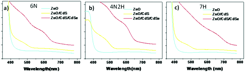 | ||
| Fig. 2 Absorption spectra of ZnO, ZnO/CdS and ZnO/CdS/CdSe, (a) 6N, (b) 4N2H, (c) 7H. | ||
Crystalline quality of ZnO nanowire
Furthermore, Raman measurement is carried out to investigate the crystalline quality of the ZnO NW array. The crystalline quality can be evaluated by the full-width at half-maximum (FWHM) of the ZnO Raman peak at 437 cm−1.31 Fig. 3 shows the Raman spectra of the ZnO NW array. Generally, the peak of ZnO (7H) has a FWHM of 9.53 cm−1, which is narrower than ZnO (4N2H) (10.01 cm−1) and ZnO (6N) (10.27 cm−1). Consequently, ZnO (7H) and ZnO (4N2H) have better crystalline quality than ZnO (6N). | ||
| Fig. 3 Raman spectra of ZnO NW array. | ||
To better understand the microstructure, single ZnO and ZnO/CdS NW of the three samples are characterized with transmission electron microscopy (TEM). Fig. 4a–c are the typical high-magnification images of the synthesized ZnO NW. The measured plane spacing (0.26 nm) is the characteristic of ZnO (002),21 confirming that the ZnO (0001) fringes are perpendicular to the wire axis. The atomic arrangements of the ZnO of the three samples are slightly different from each other. The ZnO (7H) and ZnO (4N2H) shows a much more ordered structure than the ZnO (6N), which concludes that ZnO (7H) and ZnO (4N2H) have better crystalline quality than ZnO (6N). The conclusion is consistent with the Raman result.
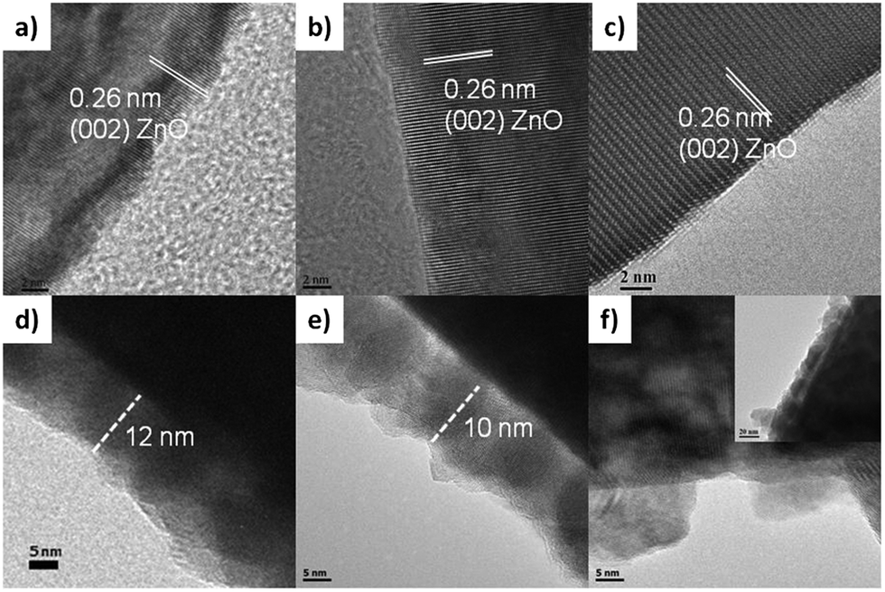 | ||
| Fig. 4 TEM images of (a) ZnO (6N), (b) ZnO (4N2H), (c) ZnO (7H), (d) ZnO/CdS (6N), (e) ZnO/CdS (4N2H) and (f) ZnO/CdS (7H). Inset of 4f is the TEM image of ZnO/CdS (7H), in which the depositing time was extended to 1 h. | ||
In addition, the influence of ZnO crystalline quality on the deposition of CdS was studied by TEM (Fig. 4d–f). Under the same deposition condition, it is obvious that a uniform CdS film covers on the surface of ZnO (6N) and ZnO (4N2H). The thickness of CdS film on ZnO (6N) is about 12 nm, whereas that on ZnO (4N2H) is about 10 nm. However, a uniform CdS film can't be deposited on the ZnO (7H) under the same condition due to the smooth surface of ZnO NW (Fig. 4f). By extending the deposition time to 1 h, a uniform CdS film forms on the surface of ZnO (7H) (the inset of Fig. 4f). As illustrated in the previous report,25 during the CdS deposition, the in situ etching of the ZnO nanowire will be carried out. The [001] plane parallels to the c axis is the most stable planes and has a lower surface energy.32 Hence, a rough surface of ZnO NW will enhance the etching of ZnO, which will benefit the deposition of CdS on the surface of ZnO NW. The behaviour of CdS deposition can also support the conclusion of crystalline quality.
Characterization of solar cell
Fig. 5a shows high-resolution TEM images of the CdS/CdSe interface regions. The result indicates that the polycrystalline CdS shell and CdSe NPs were deposited on ZnO NW. The ZnO/CdS/CdSe has been applied in solar cell with polysulfide electrolyte and CoS counter electrode (as illustrated in Fig. 5b).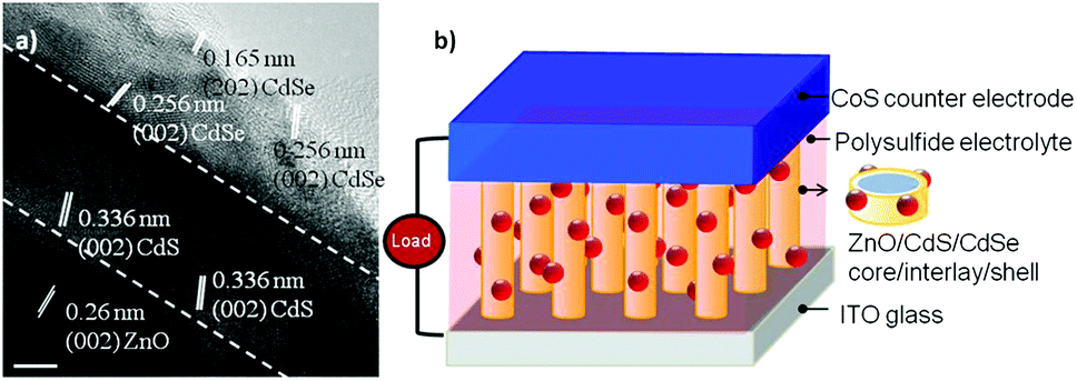 | ||
| Fig. 5 (a) High-resolution TEM images of the ZnO/CdS/CdSe interface regions, the scale bar is 5 nm. (b) Schematic diagram of the assembled solar cell. | ||
To discuss the influence of crystalline quality of ZnO on the performance of solar cell, we plotted the J–V curves of the solar cells based on ZnO (6N), (4N2H) and (7H) (Fig. 6), which have almost the same length of ZnO NW array. The photovoltaic parameters obtained from the J–V curves are shown in Table 1. The solar cell (7H) has the highest Jsc and efficiency among the three samples due to the extended absorption spectrum of ZnO/CdS/CdSe and high crystalline quality of ZnO.
 | ||
| Fig. 6 J–V curves of the solar cells based on ZnO (6N), ZnO (4N2H) and ZnO (7H). | ||
| Sample | Jsc (mA cm−2) | Voc (mV) | η (%) | FF (%) |
|---|---|---|---|---|
| 6N | 8.375 | 760 | 1.76 | 27.7 |
| 4N2H | 8.25 | 803 | 1.45 | 21.9 |
| 7H | 11.06 | 797 | 1.92 | 21.78 |
Furthermore, the dependence of the photovoltaic performance of ZnO/CdS/CdSe solar cell on the length and growth method of the ZnO NWs was investigated in detail. The length of the nanowire as a function of layers (inset of Fig. 7a) indicates that the length of the ZnO NWs increases about 2 μm per growth layer. The Jsc as a function of the length of nanowire is shown in Fig. 7a. As illustrated in the curve, the Jsc of photovoltaic is increasing as the length of nanowire getting longer. Compared to the same length, the photovoltaics of H exhibit the highest Jsc among the three samples. On the part of multiple growth of N, the Jsc increases rapidly when the length of the nanowire increases from 5.4 to 13.5 μm and slightly decreases as the length reaches 16.5 μm. The observation is consistent with the previous report, which indicates that further increase of the NW length leads to a decrease of the cell efficiency due to the decreased charge collection efficiency through a long charge pathway.29 On the other hand, the Jsc of H and NH keep increasing due to the good crystalline quality, which reduces the combination of electrons and holes.33
 | ||
| Fig. 7 (a) Short-circuit current density as a function of the length of nanowire. Inset is the length of the nanowire as a function of the growth layers. IPCE of solar cell based on ZnO obtained by (b) N, (c) NH and (d) H growth methods. | ||
To confirm the beneficial effects obtained from the increase of the length and the crystalline of ZnO NW, we measured the incident photon to current conversion efficiencies IPCE of the solar cells. Fig. 7b–d are the IPCE of ZnO prepared by N, H and NH method with the increase of the growing layer. The IPCE increases as the nanowire getting longer. The results are consistent with the corresponding Jsc showed in Fig. 6a. The solar cells based on ZnO of H method show the best performance among all of the three methods.
Considering the influence of the length and growth method of ZnO on solar cell, a best power conversion efficiency of 2.81% was obtained based on the ZnO (9H). The J–V curve of the solar cell which was prepared by using ZnO/CdS/CdSe (9H) is shown in Fig. 8, in which the Jsc is as high as 14.6 mA cm−2.
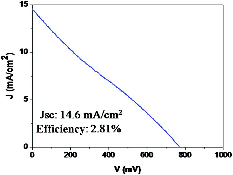 | ||
| Fig. 8 J–V curve of the solar cell based on ZnO (9H). | ||
Conclusions
In this study, we prepared ZnO nanowire electrodes based on three methods (N, NH and H). These electrodes have been applied in ZnO/CdS/CdSe core/interlay/shell solar cell with polysulfide electrolyte and CoS counter electrode. The results show that the performance of solar cell is greatly influenced by the morphology and crystalline quality of ZnO nanowire. We observe an increasing short-circuit current as follows: N < NH < H. Additionally, a best power conversion efficiency of 2.81% was obtained. These observations could have important application in designing high efficiency QD sensitized solar cell.Acknowledgements
The authors gratefully acknowledge the National Natural Science Foundation of China (Grant nos 91123032, 51003113, 61205194, and 61275171), National Basic Research Program of China (2010CB934103), and International Cooperation Program of MOST (2010DFA01180) for financial support. We are thankful to Prof. X. S. Wang and Dr J. F. Xie for their help in using the potentiostat system.Notes and references
- P. V. Kamat, J. Am. Chem. Soc., 2008, 130, 4007 CrossRef
.
- Y. Liu, A. Das, S. Xu, Z. Y. Lin, C. Xu, Z. L. Wang, A. Rohatgi and C. P. Wong, Adv. Energy Mater., 2012, 2, 47 CrossRef
- W. Kim, M. Seol, H. Kim, J. B. Miller, A. J. Gellman and K. Yong, J. Mater. Chem. A, 2013, 1, 9587 CAS
- P. D. Yang, Chem. Rev., 2010, 110, 527 CrossRef PubMed
- A. Zaban, ChemPhysChem, 2010, 11, 2290 CrossRef PubMed
- T. J. Kempa, R. W. Day, S.-K. Kim, H.-G. Park and C. M. Lieber, Energy Environ. Sci., 2013, 6, 719 CAS
- G. M. Wang, X. Y. Yang, F. Qian, J. Z. Zhang and Y. Li, Nano Lett., 2010, 10, 1088 CrossRef CAS PubMed
- K. S. Leschkies, R. Divakar, J. Basu, E. Enache-Pommer, J. E. Boercker, C. B. Carter, U. R. Kortshagen, D. J. Norris and E. S. Aydil, Nano Lett., 2007, 7, 1793 CrossRef CAS PubMed
- L. Q. Zhu, Sol. Energy, 2010, 84, 1201 CrossRef PubMed
- Y. Zhang, T. F. Xie, T. F. Jiang, X. Wei, S. Pang, X. Wang and D. Wang, Nanotechnology, 2009, 20, 155707 CrossRef PubMed
- K. H. Chen, Angew. Chem., Int. Ed., 2010, 49, 5966 CrossRef PubMed
- R. S. Aga, D. Gunther, A. Ueda, Z. Pan, W. E. Collins, R. Mu and K. D. Singer, Nanotechnology, 2009, 20, 465204 CrossRef PubMed
- J. Jean, S. Chang, P. R. Brown, J. J. Cheng, P. H. Rekemeyer, M. G. Bawendi, S. Gradecak and V. Bulovic, Adv. Mater., 2013, 25, 2789 CrossRef
- O. Niitsoo, S. K. Sarkar, C. Pejoux, S. Ruhle, D. Cahen and G. Hodes, J. Photochem. Photobiol., A, 2006, 181, 306 CrossRef CAS PubMed
- X. K. Qiu, W. X. Que, X. T. Yin, J. Zhang and J. Chen, Semicond. Sci. Technol., 2011, 26, 095028 CrossRef
- R. Zhang, Q. P. Luo, H. Y. Chen, X. Y. Yu, D. B. Kuang and C. Y. Su, ChemPhysChem, 2012, 13, 1435 CrossRef CAS PubMed
- R. Tena-Zaera, A. Katty, S. Bastide and C. Levy-Clement, Chem. Mater., 2007, 19, 1626 CrossRef CAS
- S. B. Rawal, S. Do Sung, S. Y. Moon, Y. J. Shin and W. I. Lee, Mater. Lett., 2012, 82, 240 CrossRef CAS PubMed
- H. J. Lee, J. Bang, J. Park, S. Kim and S. M. Park, Chem. Mater., 2010, 22, 5636 CrossRef CAS
- Q. X. Zhang, X. Z. Guo, X. M. Huang, S. Q. Huang, D. M. Li, Y. H. Luo, Q. Shen, T. Toyoda and Q. B. Meng, Phys. Chem. Chem. Phys., 2011, 13, 4659 RSC
- Y. Tak and K. J. Yong, J. Phys. Chem. B, 2005, 109, 19263 CrossRef CAS PubMed
- L. E. Greene, M. Law, J. Goldberger, F. Kim, J. C. Johnson, Y. F. Zhang, R. J. Saykally and P. D. Yang, Angew. Chem., Int. Ed., 2003, 42, 3031 CrossRef CAS PubMed
- L. Spanhel and M. A. Anderson, J. Am. Chem. Soc., 1991, 113, 2826 CrossRef CAS
- H. Weller, Angew. Chem., Int. Ed., 2002, 41, 1188 CrossRef
- Y. Tak, S. J. Hong, J. S. Lee and K. Yong, Cryst. Growth Des., 2009, 9, 2627 CAS
- G. Hodes, Chem. Mater., 2010, 22, 5483 CrossRef
- Z. R. Yu, J. H. Du, S. H. Guo, H. Y. Zhang and Y. Matsumoto, Thin Solid Films, 2002, 415, 173 CrossRef CAS
- Z. S. Yang, C. Y. Chen, C. W. Liu and H. T. Chang, Chem. Commun., 2010, 46, 5485 RSC
- M. Seol, H. Kim, Y. Tak and K. Yong, Chem. Commun., 2010, 46, 5521 RSC
- Q. X. Zhang, Y. D. Zhang, S. Q. Huang, X. M. Huang, Y. H. Luo, Q. B. Meng and D. M. Li, Electrochem. Commun., 2010, 12, 327 CrossRef CAS PubMed
- R. Cuscó, E. Alarcón-Lladó, J. Ibáñez, L. Artús, J. Jiménez, B. Wang and M. J. Callahan, Phys. Rev. B: Condens. Matter Mater. Phys., 2007, 75, 165202 CrossRef
- G. W. She, X. H. Zhang, W. S. Shi, X. Fan, J. C. Chang, C. S. Lee and S. T. Lee, Appl. Phys. Lett., 2008, 92, 053111 CrossRef PubMed
- K. Zhu, N. R. Neale, A. Miedaner and A. J. Frank, Nano Lett., 2006, 7, 69 CrossRef PubMed
Footnote |
| † Electronic supplementary information (ESI) available: Experimental details and general characterizations. See DOI: 10.1039/c3ra47146b |
| This journal is © The Royal Society of Chemistry 2014 |