Rational design of CuO@Cu nanostructure with tuneable morphology and electrochemical properties

Zhiyu Yang , Long Zhang, Yuxia Zhang, Yufei Zhao, Lin Jing, Yiming Yan* and Kening Sun*
Beijing Key Laboratory for Chemical Power Source and Green Catalysis, School of Chemical Engineering and Environment, Beijing Institute of Technology, Beijing, 100081, China. E-mail: yanym@bit.edu.cn; bitkeningsun@163.com

Received 26th November 2013 , Accepted 13th January 2014

First published on 14th January 2014


Abstract

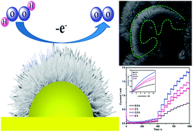
We report the fabrication of novel CuO@Cu nanostructure with tuneable morphology and electrochemical properties. An H2O2 sensor with tuneable sensing features and promising electro-oxidation of MeOH at the CuO@Cu electrode are demonstrated. The constructed H2O2 sensor based on the optimized CuO@Cu electrode has a detection limit of 11 μM.


Nanostructured metal oxides have attracted considerable attention due to their wide applications in sensing, catalysis, biomedicine and energy storage.1 Since the outstanding properties of the metal oxides are associated with their size, shape, morphology and composition, many efforts have been devoted to rationally design and synthesize various nanostructures of metal oxides for exploiting their special properties and potential applications.2 Among these metal oxides, CuO has received particular interests owning to its low cost, stability, non-toxicity and promising applications as sensors, photocatalysts, lithium-ion batteries and field emission emitters.3

Several CuO nanomaterials have been obtained with well-established strategies, including hydrothermal growth, microwave heating and chemical vapour deposition (CVD).4 For example, CuO nanoleaves have been synthesized through a template-assisted hydrothermal growth method.5 Also, CuO nanosphere was prepared by microwave-assisted hydrothermal reaction.6 Nanobelt-like CuO was grown directly on Cu substrate for lithium-ions batteries.7 Nanospindle CuO was reported by the transformation from one-dimensional Cu(OH)2 and used for detecting glucose.8 In addition, nanoplates, nanowires and nanorods of CuO have also been synthesized and used for different research purposes.9 However, the scale-up applications of CuO have been largely limited for the reported methods, mainly due to the required special instruments, low production efficiency, high reaction temperature or complex manipulation. On the other hand, CuO nanomaterial has drawn increasing attentions in electrochemical and electroanalytical applications. However, in this regard, two issues must be addressed: (1) CuO is a typical p-type semiconductor, which the relatively low conductivity is an intrinsic drawback for its electrochemical applications. To solve this problem, well-conducted carbon materials, such as mesoporous carbon, CNTs and graphene sheets, have been introduced as counterparts into CuO to improve the conductivity and enhance the performance.10 (2) Although various methods, such as electrochemical deposition, two-step electrodeposition, magnetron sputtering deposition and hydrothermal process have been proposed,11 the uniform modification of CuO nanomaterials on the electrically conductive substrate still remains challenge.

Keeping the goals in mind, we are here dedicated to prepare novel nanostructure of CuO in a simple, effective and cheap way. We demonstrate that a facile chemical etching of Cu foil surface may efficiently realize in situ generation of nanostructured CuO on Cu substrate, forming a well-characterized CuO@Cu conjunction. The resulting CuO@Cu conjunction not only possesses very low interfacial resistance, but also exhibits controllable structural and morphological properties, as well as tuneable electrochemical behaviour. We discussed the growth mechanism of the CuO@Cu nanostructure and exploited its electrochemical applications. The novel CuO@Cu electrode could be adopted to construct an electrochemical H2O2 sensor with tuneable sensing features. The results demonstrate that CuO@Cu-3.5 h shows an optimal sensitivity of 240 μA mM−1 and the lowest detection limit as low as 11 μM, superior to the previous reports.12 Meanwhile, CuO@Cu electrode could be used for electro-oxidation of MeOH. CuO@Cu-3.5 h shows its onset oxidation potential of 0.3 V vs. SCE and a promising current of 5 mA cm−2 was observed at 0.7 V, better than the reported CuO nanoparticles.13

The preparation of CuO@Cu was typically depicted in ESI. Fig. 1 presents the SEM images of the CuO@Cu samples obtained with different chemical etching times. Compared with the Cu foil without chemical etching (Fig. S1A), the CuO@Cu-0.5 h exhibits clearly porous and rough surface. A close inspection shows that the morphology contains numerous micro-clusters, which consist of organized and well-defined nanoplates (Fig. 1A′). Such nanoplates have a thickness of 60 nm and a size of ca. 100 nm. Fig. 1B shows that the sample of CuO@Cu-2 h exhibits much rougher surface, as well as uniformly dispersed regular microspheres with a size of the ca. 6 μm. The microspheres have more refined nanoplates, which are thinner and smaller than that of the sample CuO@Cu-0.5 h. With increasing the etching time, the obtained sample of CuO@Cu-3.5 h shows a higher density of microspheres on the surface. Meanwhile, the substrate supporting the microspheres was obviously observed to have a porous structure, as demonstrated in Fig. 1C′, indicating a high porosity of the substrate. In contrast, when the etching time is 6 h, the sample of CuO@Cu-6 h displays well three-dimensional structured morphology, as shown in Fig. 1D. The microspheres at the surface are much more regular and uniform, implying a deeper vertical chemical etching at the surface of Cu foil. A close view shows that the microsphere shows hedgehog-like morphology, which consists of numerous nanoneedles with a diameter of ca. 10 nm. Such a change from nanoplates to nanoneedles along with the etching time clearly indicates the morphology evolution of the resulted CuO microsphere. The chemical etching process was believed to be occurred gradually staring form the surface of copper foil with the assistant of surfactant. It is reasonable to deduce that the thickness, as well as the shape of the nanoplates, might change into numerous nanoneedles with the prolonged etching time. Similar morphology evolution mechanism has been well-investigated in the published literature.14 Therefore, it is possible to tune the surface state and morphology of the obtained CuO@Cu by simply controlling the chemical etching time.


image file: c3ra47045h-f1.tif
Fig. 1 SEM images of the CuO@Cu prepared with different reaction times (A) and (A′): 0.5 h; (B) and (B′): 2 h; (C) and (C′): 3.5 h; (D) and (D′): 6 h in solution containing 50 mM of SDS and 5.0 M of NaOH at 100 °C. The insets show the amplified SEM images of the surface morphologies of the samples.

It is interesting to understand the structural properties of the obtained CuO@Cu sample. Black powders were collected from the surface of the Cu foil and used for XRD characterizations. The XRD pattern exhibits typical diffraction peaks at 35.5 and 38.7 (seen in Fig. S2), which are assigned to the (1,1,[1 with combining macron]) and (1,1,1) crystal planes of CuO (JCPDs card no. 045-0937). Fig. 2A presents the SEM image of the cross section of a Cu foil with the formed CuO@Cu at the surface. We found that the chemical etching occurred in a thin layer of the surface. The produced CuO layer can also be apparently verified by the O elemental distribution, as shown in Fig. 2B, where the surface layer exhibits high density of O elements. Further, the uniform Cu elemental distribution implies that the CuO layer is closely covered on the conductive Cu substrate, forming the expected CuO@Cu conjunction. Such a CuO@Cu conjunction can be further confirmed by the SEM image of a cracked microsphere, as shown in Fig. 2D. We have proposed that the formation of the CuO@Cu follows a “bottom-up” growth mechanism (Scheme S1). Thus, in an ideal case, it is anticipated that the microspheres should possess a Cu-core and CuO-shell, because such a conjunction is thought to be very beneficial for electrochemical applications. This assumption is strongly supported by the mappings of O and Cu elemental distribution of a cracked microsphere, as shown in Fig. 2E and F. The high density of O elemental map could be clearly observed, as indicated by the green line, which is in well agreement with the profiles of the cracked microspheres as displayed in Fig. 2D. Furthermore, SEM images of the CuO@Cu containing semisphere and nanoplates also were presented, as shown in Fig. S1C and D. It demonstrates that the outside of the microsphere is composed of CuO layer, while the inside part comprises with the well conductive Cu-core, therefore confirming a rationally designed CuO@Cu conjunction. Such a configuration should show its advantages of uniform coverage of CuO layer on the conductive Cu substrate, as well as electrical contacting between CuO and Cu. As such, we anticipate that the facile prepared CuO@Cu with a simple chemical etching method may be used as electrode and find useful electrochemical applications.


image file: c3ra47045h-f2.tif
Fig. 2 (A) A SEM image showing the cross section of the prepared CuO@Cu conjunction. (B) and (C) show the mappings of O and Cu elemental distribution obtained at the cross section of CuO@Cu. (D) A SEM image showing the inside view of cracked CuO@Cu conjunction. (E) and (F) show the mappings of O and Cu elemental distribution obtained at the cracked CuO@Cu conjunction.

Determination of hydrogen peroxide (H2O2) is important and necessary in various fields such as clinical treatment, chemical reaction, cleanser and environmental analysis. CuO modified electrode reveals good performance as non-enzymatic electrochemical sensor of H2O2. Here, we used the prepared CuO@Cu samples as integrated electrodes and investigated their electrochemical properties for sensing H2O2. Four electrodes prepared with different etching time were compared for their H2O2 sensing performance. Fig. 3A displays the amperometric solution. The inset shows the calibration curves obtained with four electrodes, from which the sensitivity was calculated to be 110, 170, 240, and 180 μA mM−1, corresponding to CuO@Cu-0.5 h, CuO@Cu-2 h, CuO@Cu-3.5 h and CuO@Cu-6 h electrodes, respectively (Table S1). The CuO@Cu-3.5 h shows the best performance among all the tested responses of the CuO@Cu electrodes upon the addition of H2O2 electrodes. Apart from the electrochemical sensing of H2O2, we also investigated the electro-oxidation of MeOH on the CuO@Cu electrodes. MeOH could be converted into electricity by using direct MeOH fuel cells (DMFC), while the electro-oxidation of MeOH at the anode catches the key position for DMFC. Fig. S3 shows the LSVs of CuO@Cu electrode in the solution containing different concentration of MeOH. As seen, the increase of the oxidation current with the increase of MeOH concentration starts at 0.5 V vs. SCE, indicating that MeOH can be effectively electrochemically oxidized at the CuO@Cu electrode. Again, as seen in Fig. 3B, CuO@Cu-3.5 h electrode shows the highest oxidation current among all the electrodes, as well as lowest onset potential of 0.3 V vs. SCE. A promising current of 5 mA cm−2 was observed at the potential of 0.7 V at the CuO@Cu-3.5 h. As a result, we can conclude that the chemical etching derived CuO@Cu electrodes not only show prominent applications for H2O2 sensing and MeOH oxidation, but also exhibit tuneable electrochemical behaviour by controlling the etching time to obtain different CuO@Cu electrodes.


image file: c3ra47045h-f3.tif
Fig. 3 (A) Amperometric responses of the CuO@Cu electrodes to successive addition of H2O2 at 0.25 V, the inset is the calibration curve of the current response vs. H2O2 concentration. (B) LSVs recorded at CuO@Cu electrodes in 0.1 M of NaOH containing 1.0 M MeOH at a scan rate of 10 mV s−1. (C) EIS recorded at different electrodes in the 1.0 mM of potassium ferricyanide solution. (D) EIS recorded at CuO nanoparticles modified GC electrode in the 1.0 mM of potassium ferricyanide solution. (E) CVs observed at different CuO@Cu electrodes in the 1.0 mM potassium ferricyanide solution at a scan rate of 50 mV s−1. (F) CVs observed at CuO nanoparticles modified GC electrodes in the 1.0 mM potassium ferricyanide solution at a scan rate of 50 mV s−1.

In order to explain why the CuO@Cu-3.5 h electrode shows the best performance, we conducted EIS and CV measurements for clear understanding of the electrochemical properties of the electrodes. Fig. 3C shows the EIS spectra of four CuO@Cu electrodes and a roughed Cu foil electrode. The calculated interfacial electron transfer resistance Rct values of the electrodes are 56, 86, 450, 486, and 183 Ω, corresponding to CuO@Cu-0.5 h, CuO@Cu-2 h, CuO@Cu-3.5 h, CuO@Cu-6 h, and Cu foil electrodes, respectively. It suggests that Rct of the CuO@Cu electrode increases along with the increase of chemical etching time, which should be easily understood that the electrode surface was covered with much thicker layer of semiconductor CuO along with longer etching time. We also noted that the Cu foil has a high Rct than CuO@Cu-0.5 h, and CuO@Cu-2 h electrodes. This is mostly due to the acid treatment of Cu foil, leading to the formation of less conductive layer at the surface. For comparison, CuO nanoparticles were prepared by a hydrothermal method and confined onto a GC electrode. From the EIS of CuO modified electrode, the Rct was calculated to be 14[thin space (1/6-em)]600 Ω, which is apparently higher than that of CuO@Cu electrodes, as shown in Fig. 3D. Thus, it is evident that traditional modification method leads to poor electrical contacting of CuO nanoparticles with the GC electrode.

CVs can provide more electrochemical information of the examined electrodes. As shown in Fig. 3E, the potential difference of the redox peaks (ΔEp) is 0.362, 0.371, 0.385, 0.392 and 0.261 V, corresponding to CuO@Cu-0.5 h, CuO@Cu-2 h, CuO@Cu-3.5 h, CuO@Cu-6 h and Cu foil electrodes, respectively (Table S2). The observed ΔEp values are in accordance to the EIS results, because that a high value of ΔEp suggests a poor electrochemical reversibility of the measured electrode, as well as low charge transfer kinetics. Also, for comparison, the CuO modified GC electrode gives a ΔEp of 0.516 V, implying a very slow electrochemical kinetics process, as shown in Fig. 3F. Meanwhile, we noted that the values of the coulombs capacity (Qp) calculated from the electrodes are 1.12, 1.24, 2.38, 2.89 and 0.61 C, corresponding to CuO@Cu-0.5 h, CuO@Cu-2 h, CuO@Cu-3.5 h, CuO@Cu-6 h, and Cu foil electrodes (Table S2). It implies that the electro-active area of the CuO@Cu increases along with the chemical etching time. The results are reasonable because that the chemical etching help to create a rough and porous structure at the surface, consequently improving the real electro-active surface area. Thus, the EIS and CVs results suggest that, on one hand, the interfacial resistance increases along with the increase of the etching time, therefore slow down the electrochemical kinetics, on the other hand, the electro-active area also increases along with the increase of the etching time, thus providing much more electrochemical reaction sites. For an easy understating, the electrochemical process at the novel CuO@Cu electrode was illustrated in a carton picture, as shown in Scheme S2. As a conclusion, we reasonably deduced that the CuO@Cu-3.5 h shows an optimal balance between the interfacial resistance and the electro-active area, then archives the best electrochemical performance among all the electrodes.

In summary, we have demonstrated the preparation of rationally designed CuO@Cu conjunction by a facile approach. The controllable morphology and the evolvement process of the unique structure were thoroughly investigated. The nanostructured CuO was found to directly contact with the Cu substrate. Correspondingly, the CuO@Cu can not only be utilized as an integrated electrode to construct an electrochemical H2O2 sensor, showing easily tuneable sensing properties, but also be used for efficiently electrochemical oxidation of MeOH. We found that a H2O2 sensor based on the optimized CuO@Cu electrode shows a detection limit of 11 μM. The present work offers a general route to rationally design and prepare CuO@Cu with promising electrochemical properties, which could be easily extended to low-cost, broadly applicable, and large-scale synthesis of other nanostructured metal oxides for special applications, such as photocatalysis, solar cells, and energy storage.

Financial support from the National Natural Science Foundation of China (Grant nos 21175012), Ministry of Science and Technology (2012DFR40240) and the Chinese Ministry of Education (Project of New Century Excellent Talents in University) is gratefully acknowledged.

Notes and references

  1. J. Qiao, X. Mu, L. Qi, J. Deng and L. Mao, Chem. Commun., 2013, 49, 8030–8032 RSC; B. Basnar and I. Willner, Small, 2009, 5, 28–44 CrossRef CAS PubMed; R. Kou, Y. Y. Shao, D. H. Mei, Z. M. Nie, D. H. Wang, C. M. Wang, V. V. Viswanathan, S. Park, I. A. Aksay, Y. H. Lin, Y. Wang and J. Liu, J. Am. Chem. Soc., 2011, 133, 2541–2547 CrossRef PubMed.
  2. M. S. El-Deab and T. Ohsaka, Int. J. Electrochem. Sci., 2012, 7, 5115–5121 CAS; Z. Awaludin, M. Suzuki, J. Masud, T. Okajima and T. Ohsaka, J. Phys. Chem. C, 2011, 115, 25557–25567 Search PubMed.
  3. N. Leventis, N. Chandrasekaran, A. G. Sadekar, C. Sotiriou-Leventis and H. Lu, J. Am. Chem. Soc., 2009, 131, 4576–4577 CrossRef CAS PubMed; D. Praveen Kumar, M. V. Shankar, M. Mamatha Kumari, G. Sadanandam, B. Srinivas and V. Durgakumari, Chem. Commun., 2013, 49, 9443–9445 RSC.
  4. D. Keyson, D. P. Volanti, L. S. Cavalcante, A. Z. Simoes, J. A. Varela and E. Longo, Mater. Res. Bull., 2008, 43, 771–775 CrossRef CAS PubMed; D. Barreca, E. Comini, A. Gasparotto, C. Maccato, C. Sada, G. Sberveglieri and E. Tondello, Sens. Actuators, B, 2009, 141, 270–275 CrossRef PubMed.
  5. Z. H. Ibupoto, K. Khun, J. Lu and M. Willander, Appl. Phys. Lett., 2013, 102, 103701 CrossRef PubMed.
  6. G. Qiu, S. Dharmarathna, Y. Zhang, N. Opembe, H. Huang and S. L. Suib, J. Phys. Chem. C, 2012, 116, 468–477 CAS.
  7. X. Zhang, L. Yu, L. Wang, R. Ji, G. Wang and B. Geng, Phys. Chem. Chem. Phys., 2013, 15, 521–525 RSC.
  8. X. Zhang, G. Wang, X. Liu, J. Wu, M. Li, J. Gu, H. Liu and B. Fang, J. Phys. Chem. C, 2008, 112, 16845–16849 CAS.
  9. R. Li, J. Du, Y. Luan, Y. Xue, H. Zou, G. Zhuang and Z. Li, Sens. Actuators, B, 2012, 168, 156–164 CrossRef CAS PubMed; M. Mashock, K. Yu, S. Cui, S. Mao, G. Lu and J. Chen, ACS Appl. Mater. Interfaces, 2012, 4, 4192–4199 Search PubMed.
  10. M. Yang and Q. Gao, Microporous Mesoporous Mater., 2011, 143, 230–235 CrossRef CAS PubMed; H. Huang, Y. Liu, J. Wang, M. Gao, X. Peng and Z. Ye, Nanoscale, 2013, 5, 1785–1788 RSC; R. Zou, Z. Zhang, L. Yu, Q. Tian, Z. Chen and J. Hu, Chem. – Eur. J., 2011, 17, 13912–13917 CrossRef PubMed; Z. Yang, J. Feng, J. Qiao, Y. Yan, Q. Yu and K. Sun, Anal. Methods, 2012, 4, 1924–1926 RSC.
  11. Z. Wang, F. Su, S. Madhavi and X. W. Lou, Nanoscale, 2011, 3, 1618–1623 RSC.
  12. S. Weng, Y. Zheng, C. Zhao, J. Zhou, L. Lin, Z. Zheng and X. Lin, Microchim. Acta, 2013, 180, 371–378 CrossRef CAS; F. Wang, A. Kalam, L. Chang, D. Xie, A. S. Al-Shihri and G. Du, Mater. Lett., 2013, 92, 96–99 CrossRef PubMed.
  13. D. R. Kauffman, P. R. Ohodnicki, B. W. Kail and C. Matranga, J. Phys. Chem. Lett., 2011, 2, 2038–2043 CrossRef CAS.
  14. X. Chen, N. Q. Zhang and K. N. Sun, J. Phys. Chem. C, 2012, 116, 21224–21231 Search PubMed; Y. Li, D. Cao, Y. Liu, R. Liu, F. Yang, J. Yin and G. Wang, Int. J. Hydrogen Energy, 2012, 37, 13611–13615 CrossRef CAS PubMed.

Footnotes

Electronic supplementary information (ESI) available: Experimental details, XRD, LSVs and Schemes. See DOI: 10.1039/c3ra47045h
These two authors have the same contribution to this work.

This journal is © The Royal Society of Chemistry 2014
Click here to see how this site uses Cookies. View our privacy policy here.