DOI:
10.1039/C3RA46666C
(Paper)
RSC Adv., 2014,
4, 7627-7633
Free standing silica thin films with highly ordered perpendicular nanopores†
Received
27th November 2013
, Accepted 7th January 2014
First published on 8th January 2014
Abstract
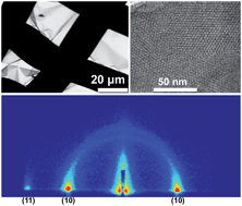
The synthesis of mesoporous silica thin films on nontraditional conductive substrates using an electro-assisted self-assembly (EASA) technique is described. This work extends prior demonstrations of EASA by exploring the effects of precursor sol pH, temperature, and substrate roughness and describes a new approach to synthesizing a mesoporous silica film that is detachable from the substrate. The latter uses a conductive polymer as a planarization layer for successful EASA on indium-tin oxide coated glass (ITO) and as a sacrificial layer that can be subsequently dispersed in water to release the silica film. This is a particularly important development because it opens up possibilities for synthesizing perpendicularly aligned nanoporous silica on a broad range of surfaces and non-conductive substrates and producing free standing nanostructured thin films. The silica films that are produced have well ordered hexagonally packed mesopores that are vertical to the substrate surface. The thicknesses of these mesoporous silica films were examined by scanning electron microscopy (SEM) and determined to be controllably variable between ∼100 and 200 nm. Transmission electron microscopy (TEM) showed organized porous structural features that were approximately 3 nm in diameter. Grazing-incidence small angle X-ray scattering (GISAXS) analysis yielded an ∼4.2 nm pore-to-pore distance and confirmed that a p6mm orientation persisted throughout the 6 cm2 mesoporous silica film samples.
1. Introduction
Mesoporous silica materials have drawn a great deal of attention because of their process-tunable pore diameters that can be varied from 2 to 30 nm, large surface areas and pore volumes,1–5 and stability in air and liquids. These advantages make them ideal hosts or “hard templates” for the preparation of ordered nanostructure arrays of metals,6 metal oxides,7,8 semiconductor materials,9–11 and carbon-based nanostructures,6 with applications in catalysis, electrochemistry, semiconductor devices, and photovoltaics. Moreover, the fabrication of films with well defined nanopores oriented perpendicular to the substrate surface allows direct through-film access and opens up new application areas where, for example, electrical or molecular transport along the length of the pores is important. These include nanowire arrays for electronic devices, solution based selective sensors and preconcentrators.12 Furthermore, the ability to detach the mesoporous films from the solid substrates will yield high pore density films that can be used as membranes or biosensors.13 Synthesizing free-standing through-film nanoporous arrays with well defined size and orientation across large areas is extremely desirable and very challenging.
Mesoporous silica thin films are often prepared by dip-coating, printing, or spin-coating silica-based precursors on to flat substrates.14 Such processes generally lead to randomly oriented pores or limited domain ranges with oriented pores. Evaporation induced self-assembly (EISA)13 is a versatile method for preparing films on flat surfaces. However, the mesopores of the EISA films13,15 generally form parallel to the substrate surface. Combining EISA with an applied field16–18 has been demonstrated as a method for achieving perpendicular pore orientation. In 1997, Firouzi19 and Tolbert20 created an aligned surfactant-silica mesophase on the centimeter scale by applying a high magnetic field during film formation. Yamauchi21 further demonstrated the influence of high magnetic fields on the orientation of a block copolymer surfactant that was used to form nanochannels in silica films. Although, these studies demonstrated the possibility of producing perpendicularly oriented pores, the use of a high magnetic field may not be practical for the synthesis of large area films. Richman22 obtained vertically oriented hexagonally packed nanoporous silica films by nanometer-scale epitaxy. This method required a precise lattice match between the pores of the surfactant-silica film and the cubic mesoporous substrates. Teng23 developed a Stöber-solution growth approach to obtain mesoporous silica thin films with perpendicular channels. However, the film formation took several days under strictly controlled high temperatures due to the slow film growth speed (2 nm h−1). Other approaches for orienting pores perpendicular to the substrate include optical lithography,24 ion track etching24 electrochemical etching,25 and anodization.24 These methods are usually limited to >10 nm pores or disordered pore structures.
Recently, Walcarius26 and Goux27 developed an intrinsically simple and fast electro-assisted self-assembly (EASA) method to prepare silica films with pores that are orthogonal to the surface of metals, glassy carbon, and conductive metal oxide substrates. EASA exploits the electrochemically driven self-assembly of cationic surfactant molecules,27 the electro-generation of hydroxyl ions,26 and silica condensation26 at the cathode surface. The first process leads to ordered surfactant self-assembly and alignment, the second catalyzes sol polycondensation and the third results in silica sol condensation around the surfactant nanostructures. The net result is the formation of a thin silica film consisting of hexagonally packed nanochannels that are aligned perpendicular to the cathode surface. EASA requires a conductive substrate that can serve as the cathode. Mesoporous silica film formation on gold, platinum, copper, indium tin oxide, and glassy carbon substrates has been successfully demonstrated over 10 mm2 areas. Pore sizes are varied between 2.6 and 3.1 nm depending on the carbon chain length of the alkyltrimethylammonium bromide surfactant CnTAB (n = 14–18).
Thus far, EASA has been performed only on conductive substrates. In addition, while removal of silica films for electron microscopy was accomplished by mechanically scraping the cathode, this removal process is not a practical method for obtaining large, substrate free, film areas for further study or applications. Furthermore, the adhesion28 of thin silica films to noble metal (such as Au, Pt, etc.) substrates is weak and leads to defects in the form of cracks. The local detachment from the substrate causes changes in the film morphology during surfactant removal due to the reduction in the surface energy.29 Conductive metal oxides present a surface that could be used with EASA with advantages that include good adhesion to silica thin film and good conductivity. However, the effect of the relatively high surface roughness30 of glass-coated conductive metal oxide substrates on the formation of uniform perpendicular oriented mesoporous films is undetermined. This roughness can be reduced by coating the metal oxide with conductive polymers.31
This paper describes the successful synthesis of mesoporous silica films on two non-traditional conductive substrates using the EASA technique and the subsequent detachment of the film from the substrate. Poly(3,4-ethylenedioxythiophene):poly(styrenesulfonate) (PEDOT:PSS) is a conductive polymer that was spin coated onto surfaces such as indium-tin oxide (ITO) to improve the surface flatness and adhesion of silica. This PEDOT:PSS coated ITO will be referred to as P-ITO. The second substrate investigated in this work is a heavily doped n-type silicon wafer, also with a flat surface32 and good attachment to silica.28 Synthesis and EASA conditions are optimized and explanations are given for the successful formation of silica films with mesopores oriented perpendicular to the substrate surface. The process for detaching or lifting off the mesoporous silica film from the P-ITO substrate is also described.
2. Experimental
Synthesis of the mesoporous silica films occurs in different stages starting with preparation of the precursor sol, followed by preparation of the conductive substrates, and ending with electro-assisted self-assembly of rod-shaped surfactant micelles and polycondensation of silica around the micelles at the cathode/substrate surface. Each stage required optimization and was performed as described below. All chemicals were used as purchased without further purification.
2.1. Preparation of precursor sol
A solution was prepared by mixing 0.82 g (2.18 mmol) cetyltrimethylammonium bromide (CTAB, 99%, Fluka, Denmark), 20 mL ethanol (95%, Pharmco Products Inc., CT, USA), and 20 mL aqueous 0.1 M NaNO3 (98%, J.T. Baker Chemical Co., NJ, USA) and adjusting the pH with HCl (37%, Pharmco-AAPER Subsidiaries of Commercial Alcohols Inc., CT, KY, USA). To this solution, 1.52 mL (1.42 g, 6.80 mmol) tetraethyl orthosilicate (TEOS, 98%, Aldrich, MO, USA) was added under stirring. The resulting precursor sol had an optimum [CTAB]:[TEOS] ratio of 0.32 and was allowed to hydrolyze for 2.5 hours.26,27 Fresh precursor sol was made for each experiment. The role of the NaNO3 in the precursor sol was to increase the conductivity of the sol and subsequently facilitate the EASA process. The pH and temperature of the precursor sol were varied to determine optimum conditions for the formation of ordered silica mesopores.
2.2. Preparation of substrates
The conductive substrates used in this work are an indium-tin oxide coated glass (ITO) (Colorado Concept Coatings, CO, USA) with a surface resistivity of ∼25.6 ohms (measured in lab), indium-zinc oxide coated glass (IZO) (Colorado Concept Coatings, CO, USA) with a surface resistivity of ∼15.2 ohms (measured in lab), PEDOT-PSS (Clevios P VP al 4083, Germany) modified ITO (P-ITO) and a heavily doped conductive silicon wafer n-Si [100] with phosphorus dopants, 14–22 ohm cm (University Wafer, MA, USA). ITO and IZO are cleaned by sequential sonication in acetone and isopropanol for 5 min in each solvent followed by oxygen plasma treatment for 5 min. The P-ITO is prepared by first filtering PEDOT:PSS through a Pall Acrodisc 0.45 μm syringe filter (CELLTREAT Scientific Products, LLC, MA, USA), then depositing two layers of PEDOT:PSS by spin coating each layer successively at 6000 rpm onto a plasma cleaned ITO surface, and finally annealing the PEDOT:PSS-ITO at 120 °C for 20 min. The last substrate, n-Si [100] wafer, is etched in 5% HF solution for 3 minutes to remove the surface oxide layer and improve conductivity across the surface. All substrates are approximately 2.54 cm × 2.54 cm squares.
2.3. Electro-assisted self-assembly (EASA)
The electrochemical system consists of a 2.54 cm × 2.54 cm planar graphite electrode (anode, counter electrode) and an ITO, IZO, P-ITO or silicon wafer substrate (cathode, working electrode) that is submerged in the precursor sol solution. The two electrodes are held parallel to each other, one inch apart. A Model 362 Scanning Potentiostat (Princeton Applied Research, TN, USA) is used to apply the current needed for aligning CTAB molecules and generating the hydroxyl ions essential for polycondensation of silica thin films at the substrate surface. The current is set at a constant current of 0.75 mA cm−2 substrate and the EASA time is varied between 10 and 20 seconds (as previously optimized).26,27
2.4. Characterization
After EASA, the resulting structure consisted of CTAB molecules surrounded by silica. The final step to producing mesoporous silica films involved removal of the CTAB to create open pores. This is accomplished by immersing the sample in a 0.01 M HCl ethanol–water solution (50
:
50 v/v) for 30 minutes under stirring.26,27 FTIR characterization confirmed the complete removal of surfactant from the silica film on Si wafer (see ESI†). For metal oxides, the CTAB can also be removed by calcination at 300 °C for 30 min.
The silica film's pore-to-pore distance and pore alignment on the silicon wafer and P-ITO substrates are characterized by Grazing Incidence Small Angle X-ray Scattering (GISAXS) using a Nonius Kappa-CCD diffractometer equipped with an Apex II CCD detector (copper cathode λαI = 0.154184 nm).
Cross-sectional scanning electron microscope (SEM) images of the silica films to confirm film formation and determine thickness are obtained at a 13° tilt using a JEOL JSM-7000F field emission SEM (JEOL USA, Inc. MA, USA) with an EDAX Genesis energy dispersive X-ray spectrometer in TSL electron backscatter diffraction mode. Top views showing the size and uniformity of the silica mesopores are obtained with a Phillips CM200 transmission electron microscope (Amsterdam, Netherlands) coupled with a Princeton Gamma-Tech prism energy dispersive X-ray spectrometer. TEM samples were prepared by either using a razor blade to mechanically scrape the silica template from the cathode onto the TEM grid or using a liftoff method (described later) that preserves knowledge of the film orientation.
The surface roughness of cleaned substrates is measured with a Bruker Nanoscope III multimode atomic force microscopy (AFM) (CA, USA) using SiN tips with tip curvature less than 10 nm and operating in tapping mode. The surface roughness is also measured by a Tencor P-10 Surface Profiler (CA, USA).
3. Results and discussion
Reactions pertinent to the preparation of silica films with mesopores oriented perpendicular to the substrate surface are shown in Scheme 1. The first step (Scheme 1A) is the acid catalyzed hydrolysis of TEOS. The pH of the precursor sol and the hydrolysis temperature play important roles in the subsequent formation of the desired mesoporous silica films. The second step is the EASA process which involves the simultaneous electrochemically driven self assembly of cationic surfactants, electro-generation of hydroxide ions (Scheme 1B) and hydroxyl ions catalyzed polycondensation of silica (Scheme 1C) at the cathode/substrate surface.
 |
| Scheme 1 Reactions pertinent to the formation of ordered and perpendicularly aligned mesopores. (A) Acid-catalyzed hydrolysis of TEOS. (B) Electro-generation of hydroxyl ions on cathode surface. (C) Hydroxyl ions catalyzed silica sol condensation on cathode surface. | |
The effect of precursor sol conditions and substrate surface roughness on the formation of aligned and ordered mesopores are investigated. The resultant silica films are characterized with respect to their thickness, pore size, orientation, and uniformity.
3.1. Optimization of mesoporous silica film formation
3.1.1. Effect of sol pH.
The pH of the precursor sol is important for the formation of uniform silica films because there must be sufficient amounts of hydrolyzed TEOS for polycondensation, but without a large excess of H+ in solution. The optimum pH is determined by maintaining a constant temperature of 25 °C and varying the solution pH. TEM images of the silica films formed on the P-ITO substrate surface are shown in Fig. 1. At pH = 1.0 and 2.0, silica particles (Fig. 1A) and a multilayer silica film (Fig. 1B) are observed, respectively. At pH < 2, silica condensation can occur in the bulk solution through an acid catalyzed mechanism33 and lead to the formation of silica particles. Since this pH is below the isoelectric point of silica, the particles are positively charged34 and are attracted to and deposited on the cathode/substrate. At pH = 3.0, the desired silica films with highly ordered aligned nanopores were obtained (Fig. 1C and D). At pH = 4.0 and higher (not shown), no silica film is formed. We speculate that an insufficient amount of hydrolyzed TEOS to create a film is produced at this pH.
 |
| Fig. 1 TEM images of silica films formed on P-ITO substrates using precursor sols maintained at 25 °C and different pHs. (A) pH = 1.0, (B) pH = 2.0, (C) and (D) pH = 3.0. | |
3.1.2. Effect of sol temperature.
EASA was performed using the optimized precursor sol pH (pH 3). Fig. 2 shows TEM images of the top view of silica films formed on a P-ITO substrate. Temperatures of 15 °C and 35 °C (Fig. 2A and C) produced silica films with varying pore patterns and domains. The 25 °C precursor sol produced a regular array of hexagonally close packed pores across the entire TEM viewing area (Fig. 2B).
 |
| Fig. 2 TEM images of silica films formed on P-ITO substrates using pH = 3.0 precursor sols and different temperatures (A) T = 15 °C, (B) T = 25 °C, and (C) T = 35 °C. | |
3.1.3. Effect of substrate surface roughness.
The relative roughness of ITO, P-ITO, and IZO coated glass and heavily doped silicon wafer are qualitatively evaluated by top view SEM and quantified using AFM. The SEM micrographs in Fig. 3 show that ITO possesses the roughest surface and that the PEDOT:PSS coating does indeed planarize the ITO surface. These observations are reflected in the AFM root mean square values (RMS) of 4.98 ± 0.37 nm (ITO), 0.96 ± 0.02 nm (P-ITO), 0.08 ± 0.01 nm (Si wafer), and 0.96 ± 0.03 nm (IZO) over a 500 nm × 500 nm area. (The IZO image also shows the presence of several raised particle-like features which significantly affect the peak-to-valley values and thus these numbers are not reported here.)
 |
| Fig. 3 SEM (top view) images of (A) ITO, (B) P-ITO, (C) heavily doped silicon wafer and (D) IZO. | |
TEM images of silica films formed on each substrate are shown in Fig. 4. While mesopores are sometimes observed in silica films prepared on ITO coated glass, the quality is low with considerable pore disorder and mis-orientation. In contrast, silica films on PEDOT:PSS modified ITO and heavily doped silicon wafer have hexagonally packed mesopores that extend laterally over several hundred square nanometers. Surprisingly, the silica film on IZO does not exhibit a well defined array of pores despite its comparable RMS to P-ITO. The AFM image of the IZO substrate surface shows small grain sizes that are not apparent on the P-ITO surface (data not shown). The large tilt angles associated with these small grain sizes and their dense packing may hinder coherent micelle assembly during the EASA process. It is possible that substrate surface roughness and the size and density of surface convolutions play an important role in the successful formation of silica films with uniformly aligned mesopores.
 |
| Fig. 4 TEM images of silica films formed on (A) ITO, (B) P-ITO, (C) heavily doped silicon wafer and (D) IZO at precursor sol TEOS hydrolysis of pH = 3.0 and T = 25 °C. | |
3.2. Structural characterization
The orientation of mesopores in silica thin films formed on P-ITO and heavily doped silicon wafer substrates was characterized using 2D GISAXS. The results in Fig. 5 show scattering spots in the equatorial plane in the 2D GISAXS patterns of mesoporous silica films and are indicative of a high level of mesostructural order in the silica film and a vertical orientation of mesopores over several square centimeters. These spots arise from scattering of the (11) and (10) planes of the pore arrays in the silica thin films on P-ITO and Si wafer substrates. The same peaks are also visible in the one dimensional GISAXS traces derived from Fig. 5A and B and shown in Fig. 5C and D. The scattering maximum appears at qmax = 1.722 ± 0.009 nm−1 and qmax = 1.699 ± 0.009 nm−1 for the mesoporous silica films on P-ITO and Si wafer, respectively. From this, the pore periodicities of the samples are found to be d = 3.65 ± 0.02 nm and 3.67 ± 0.02 nm for mesoporous silica films on P-ITO and Si wafer, respectively. Taking into account the hexagonal pore pattern, the pore-to-pore distances were determined to be 4.22 ± 0.02 nm and 4.23 ± 0.02 nm. The difference in mesopores sizes measured for the two substrates is <0.5%. These GISAXS results confirm that the hexagonal patterns in the TEM images of Fig. 1D, 2B, and 4B represent vertical pores and not Moire patterns produced by overlapping stripes from the side view of overlaid hexagonally packed mesopores. The faint rings observed in Fig. 5A and B are due to spherical silica particles that form on the surface of the mesoporous silica thin films via silica condensation in the bulk solution.29
 |
| Fig. 5 2D GISAXS pattern of mesoporous silica thin films on different substrates (A) P-ITO and (B) heavily doped silicon wafer; 1D GISAXS pattern of mesoporous silica thin films on (C) P-ITO and (D) heavily doped silicon wafer. Precursor sol pH = 3.0 and T = 25 °C. | |
The silica films formed on P-ITO and heavily doped silicon wafer substrates were further examined by SEM. Cross sectional SEMs in Fig. 6A and B allowed the various layers in the films to be identified and from this, a growth rate could be obtained. Using optimized pH and temperature and holding the current between electrodes constant at 0.75 mA cm−2 for 10–20 s during EASA growth resulted in the formation of 100–200 nm thick films (growth rate of 10 nm s−1) on both the P-ITO and heavily doped Si wafer substrates. EDX confirmed that the top layer in both SEM images was silica. TEM images show that the silica films formed on both substrates have well-ordered hexagonally packed mesopores that are ∼3 nm in diameter (Fig. 6C and D). This is in good agreement with the GISAXS pore-to-pore distance of ∼4.2 nm. Uniform mesopores are observed when different regions of the 6.5 cm2 silica film are examined. Fig. 6E shows a TEM image of the silica film with a striped pattern that is ∼100 nm in length and ∼3 nm in width. These dimensions correspond to the measured thickness of the silica film and the size of the mesopores and thus this image is attributed to a cross section view of the silica film. In combination, the GISAXS measurements and electron micrographs provide evidence that the mesopores in the silica film are oriented perpendicular to the substrates' surface. The TEM images of silica film on P-ITO and silicon wafer in Fig. 4 and 6 are from different samples and illustrate the reproducibility of the EASA process. The high resolution images confirm the quality of the close packed mesopores.
 |
| Fig. 6 Cross sectional SEM images of silica thin films on different substrates (A) P-ITO and (B) heavily doped silicon wafer; TEM images (top view) of silica templates on (C) P-ITO and (D) heavily doped silicon wafer and (E) cross section of a silica template on P-ITO. Precursor sol pH = 3.0 and T = 25 °C. | |
3.3. Using PEDOT:PSS to obtain free standing silica thin films
The ability to form mesoporous silica films on substrates coated with conducting organics such as PEDOT:PSS greatly expands the range of substrates and, hence, novel applications. The polymer can be used to planarize rough surfaces and to impart conductivity to insulating substrates. If desired, the PEDOT-PSS coating on P-ITO can be easily eliminated by calcining at 300 °C for 30 min. This effectively results in a well organized nanoporous silica thin film in contact with a relatively rough metal oxide substrate or an insulating substrate.
Perhaps more importantly, mesoporous film formation on a PEDOT:PSS coated substrate opens up the possibility of film liftoff to yield a free standing nanoporous silica film or for direct transfer to an alternative surface on which it would not normally be possible to synthesize such a film. To demonstrate liftoff, narrow strips of two-sided adhesive tape are attached to the outer periphery of a TEM grid. The grid is then pressed onto the surface of the mesoporous silica thin film formed on a PEDOT:PSS coated ITO substrate to adhere and liftoff the silica film only. The low magnification TEM image of Fig. 7A shows a large section of the silica film positioned on the TEM copper grid. Pore uniformity is clearly maintained as demonstrated by the higher magnification image shown in Fig. 7B. This film transfer has the additional benefit of allowing examination of the pores from the side of the film that was originally attached to the substrate and further confirmed the nanopores' vertical orientation and the interpretation of TEM results shown in earlier figures as “top view”. The silica film can also be detached by submersing the sample in water to disperse the PEDOT:PSS and sonicating for 90 s at 135 W and 42 kHz. The released film floated to the surface and was ‘fished out’ with a TEM grid. Similar results (see ESI†) to those shown in Fig. 7 are obtained. Again, in spite of the unoptimized detachment process, the structural integrity of the resulting free standing nanoporous silica film is maintained.
 |
| Fig. 7 TEM of silica film after “liftoff” from P-ITO substrate. (A) Low magnification image showing a small square of the TEM grid (dark straight rectangles) with a section of silica film and (B) high magnification image of the mesoporous silica film. | |
4. Conclusions
Silica thin films with ∼3 nm mesopores that are hexagonally packed and aligned perpendicularly to the surface were rapidly synthesized on P-ITO and heavily doped silicon wafer substrates using an electro-assisted self assembly method. Optimum conditions that led to formation of mesoporous films on these surfaces were identified. TEM and GISAXS confirmed the presence of highly ordered mesopores aligned perpendicular to the substrate surface. The use of a PEDOT:PSS layer opened up the possibility for producing aligned mesopores on a much broader range of surfaces and non-conductive substrates. In addition to being a nontraditional conductive substrate, the PEDOT:PSS coated substrates have the additional feature of providing a facile route for detaching and transferring the silica film to other substrates and for forming free standing mesoporous silica thin films.
Acknowledgements
This material is based upon work supported by the National Science Foundation sponsored Renewable Energy Material Research Science and Engineering Center (REMRSEC) under DMR-0820518. We gratefully acknowledge the assistance of John Chandler and Gary Zito for electron microscopy, David Grosso for GISAXS, Tom Brenner for AFM measurements, and all REMRSEC members for insightful discussions.
References
- C. T. Kresge, M. E. Leonowicz, W. J. Roth, J. C. Vartuli and J. S. Beck, Nature, 1992, 359, 710 CrossRef.
- D. Zhao, J. Feng, Q. Huo, N. Melosh, G. H. Fredrickson, B. F. Chmelka and G. D. Stucky, Science, 1998, 279, 548 CrossRef.
- Y. Sakamoto, I. Diaz, O. Terasaki, D. Zhao, J. Perez-Pariente, J. M. Kim and G. D. Stucky, J. Phys. Chem. B, 2002, 106, 3118 CrossRef.
- J. Fan, C. Yu, T. Gao, J. Lei, B. Tian, L. Wang, Q. Luo, B. Tu, W. Zhou and D. Zhao, Angew. Chem., Int. Ed., 2003, 42, 3146 CrossRef PubMed.
- C. Gao, Y. Sakamoto, K. Sakamoto, O. Terasaki and S. Che, Angew. Chem., Int. Ed., 2006, 45, 4295 CrossRef PubMed.
- F. Kleitz, S. Choi and R. Ryoo, Chem. Commun., 2003, 2136 RSC.
- C. Dickinson, W. Zhou, R. P. Hodgkins, Y. Shi, D. Zhao and H. He, Chem. Mater., 2006, 18, 3088 CrossRef.
- K. Jiao, B. Zhang, B. Yue, Y. Ren, S. Liu, S. Yan, C. Dickinson, W. Zhou and H. He, Chem. Commun., 2005, 5618 RSC.
- S. H. Woo and D. Whang, J. Korean Phys. Soc., 2009, 54, 152 CrossRef.
- N. R. B. Coleman, M. A. Morris, T. R. Spalding and J. D. Holmes, J. Am. Chem. Soc., 2001, 123, 187 CrossRef.
- N. R. B. Coleman, N. O'Sullivan, K. M. Ryan, T. A. Crowley, M. A. Morris, T. R. Spalding, D. C. Steytler and J. D. Holmes, J. Am. Chem. Soc., 2001, 123, 7010 CrossRef PubMed.
- P. Xu, H. Yu and X. Li, Anal. Chem., 2011, 83, 3448 CrossRef PubMed.
- P. Innocenzi and L. Malfatti, Chem. Soc. Rev., 2013, 42, 4198 RSC.
- D. Grosso, F. Cagnol, G. J. de A. A. Soler-Illia, E. L. Crepaldi, H. Amenitsch, A. Brunet-Bruneau, A. Bourgeois and C. Sanchez, Adv. Funct. Mater., 2004, 14, 309 CrossRef.
- H. Yang, N. Coombs and G. A. Ozin, J. Mater. Chem., 1998, 8, 1205 RSC.
- M. Lukaschek, D. A. Grabowski and C. Schmidt, Langmuir, 1995, 11, 3590 CrossRef.
- K. Amundson, E. Helfand, X. Quan and S. D. Hudson, Macromolecules, 1994, 27, 6559 CrossRef.
- W. Schnepp, S. Disch and C. Schmidt, Liq. Cryst., 1993, 14, 843 CrossRef.
- A. Firouzi, D. J. Schaefer, S. H. Tolbert, G. D. Stucky and B. F. Chmelka, J. Am. Chem. Soc., 1997, 119, 9466 CrossRef.
- S. H. Tolbert, A. Firouzi, G. D. Stucky and B. F. Chmelka, Science, 1997, 278, 264 CrossRef.
- Y. Yamauchi, M. Sawada, T. Noma, H. Ito, S. Furumi, Y. Sakka and K. Kuroda, J. Mater. Chem., 2005, 15, 1137 RSC.
- E. K. Richman, T. Brezesinski and S. H. Tolbert, Nat. Mater., 2008, 7, 712 CrossRef PubMed.
- Z. Teng, G. Zheng, Y. Dou, W. Li, C. Mou, X. Zhang, A. M. Asiri and D. Zhao, Angew. Chem. Int. Ed., 2012, 51, 2173 CrossRef PubMed.
- P. Stroeve and N. Ileri, Trends Biotechnol., 2011, 29, 259 CrossRef PubMed.
- Z. P. Huang, N. Geyer, L. F. Liu, M. Y. Li and P. Zhong, Nanotechnology, 2010, 21, 465301 CrossRef PubMed.
- A. Walcarius, E. Sibottier, M. Etienne and J. Ghanbaja, Nat. Mater., 2007, 6, 602 CrossRef PubMed.
- A. Goux, M. Etienne, E. Aubert, C. Lecomte, J. Ghanbaja and A. Walcarius, Chem. Mater., 2009, 21, 731 CrossRef.
-
J. W. Dini, Electrodeposition: The Materials Science of Coatings and Substrates, Noyes Publications, Norwich, NY, 1993 Search PubMed.
- S. Sayen and A. Walcarius, Electrochem. Commun., 2003, 5, 341 CrossRef.
- G. Kavei, Y. Zare and M. A. Gheidari, Scanning, 2008, 30, 232 CrossRef PubMed.
- S. Na, G. Wang, S. Kim, T. Kim, S. Oh, B. Yu, T. Lee and D. Kim, J. Mater. Chem., 2009, 19, 9045 RSC.
- G. Udupa and B. K. A. Ngoi, Proc. Annu. Meet. – Am. Soc. Precis. Eng., 2000, 421 Search PubMed.
-
C. J. Brinker, and G. W. Scherer, Sol-Gel Science-The Physics and Chemistry of Sol-Gel Processing, Academic Press, Boston, MA, 1990 Search PubMed.
-
Colloidal Silica: Fundamentals and Applications, ed. H. E. Bergna and W.O. Roberts, Taylor and Francis Group, Boca Raton, FL, 2006 Search PubMed.
Footnote |
† Electronic supplementary information (ESI) available. See DOI: 10.1039/c3ra46666c |
|
This journal is © The Royal Society of Chemistry 2014 |
Click here to see how this site uses Cookies. View our privacy policy here.