Yiming Tang,
Yun Hau Ng*,
Jung-Ho Yun and
Rose Amal*
ARC Centre of Excellence for Functional Nanomaterials, School of Chemical Engineering, The University of New South Wales, Sydney, New South Wales 2052, Australia. E-mail: yh.ng@unsw.edu.au; r.amal@unsw.edu.au
First published on 2nd December 2013
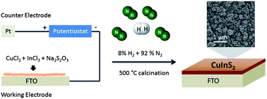
n-type CuInS2 thin films were fabricated by a one-step electrodeposition of Cu/In/S precursors on a transparent fluorine-doped tin oxide (FTO) substrate followed by calcination in a mixture of N2 and H2 at 500 °C without the need of toxic H2S gas for sulfurization. The analyses of structural and optical properties revealed that tetragonal chalcopyrite CuInS2 thin films were obtained when heat treated in a mixture of 8% H2 and 92% N2; whereas calcination in pure N2 resulted in the formation of CuInS2 with a considerable amount of In2O3 and CuxS impurities. The synthesized n-CuInS2 thin film has an optical bandgap of 1.3 eV with the conduction band at ca. −1.2 V vs. Ag/AgCl at pH 6.5. The heat treatment in a mixture of H2 and N2 provided a reducing atmosphere to suppress the oxide formation of the electrodeposited Cu/In/S elements. It also increased the donor density of CuInS2 sixfold by increasing the density of the sulfur vacancies (known to be electron donors) at the grain surface. As a result of the improved purity and increased donor density, the hydrogen treated CuInS2 thin film yielded a photocurrent density of ∼8 mA cm−2 at 0.5 V vs. Ag/AgCl in 0.25 M Na2S and 0.35 M Na2SO3 under visible light illumination, which is a fourfold enhancement as compared to that obtained from the CuInS2 film calcined in pure N2.
Fabrication of chalcopyrite thin films traditionally involves a high-vacuum evaporation/deposition technique.12 To reduce the high preparation cost associated with the high vacuum, a two-step process has been developed where the metallic components (Cu, In, Ga, Zn or Sn) are initially deposited on a conducting substrate at milder conditions followed by a sulfurization step at a high temperature.13 A variety of techniques has been used for metallic deposition such as sputtering,14 spray pyrolysis,15 molecular beam deposition16 and electrodeposition.2 In the subsequent sulfurization process at a high temperature, H2S or elemental sulfur are the most used precursors despite their toxicity in the gas phase. Regardless of the deposition technique of the metallic precursors and the source of sulfurization, an annealing process is necessary to crystallize the deposited components into their chalcopyrite structure. The morphology (formation of pinholes) as well as the film stability (adherence) can be optimized by altering the annealing conditions.17
Considering the advantages of using the non-vacuum and two-step film synthesis, electrodeposition is an attractive option for depositing the metallic components of CuInS2 since it can proceed at low/room temperature, requires a simple equipment setup, and generates no waste emission. As a greener fabrication process is increasingly required, efforts have been made in excluding H2S throughout the synthesis of chalcopyrite semiconductor thin films.18–20 This motivated us to investigate the simultaneous deposition of sulfides during the metal deposition in this work eliminating the use of H2S in the subsequent high temperature annealing. We have recently reported the formation of a CuInS2–TiO2 nanotube composite using a square wave pulse electrodeposition technique that enables the penetration of soluble CuInS2 (CuCl2, InCl3 and Na2S2O3) precursors into the capillary force resistant pore channels of the TiO2 nanotubes for deposition.21 Despite the successful synthesis of TiO2 nanotubes completely wrapped with CuInS2 nanoparticles, the formation of In2O3 impurities was observed. The oxidation of the deposited metallic In induced a stoichiometric imbalance of metallic Cu:
In ratio and, therefore, promoted the formation of oxides of Cu or CuxS. Thus, the suppression of the formation of In2O3 during the synthesis is important. In this study, we attempted to fabricate CuInS2 thin film using a single-step electrodeposition method followed by crystallization of the deposited precursors in a reducing atmosphere. Specifically, the effects of using a mixture of N2 and H2 on the suppression of impurities as related to the electronic properties and the PEC performance is discussed.
The electrochemical impedance experiments were carried out in a three-electrode electrochemical system with a 0.5 M K2SO4 electrolyte (pH 6.3–6.5). The counter and the reference electrodes were platinum wire and Ag/AgCl, respectively. The Mott–Schottky plot of the CuInS2 film was measured using a potentiostat (Autolab Model PGSTAT 12) with a frequency response analyzer (Autolab FRA2 modules). The frequencies of 10 Hz, 100 Hz and 1000 Hz were used for the measurements. Additionally, the applied potential was scanned from −1 V to 0.1 V (vs. Ag/AgCl) with a scan rate 50 mV s−1.
![]() | ||
Fig. 1 XRD patterns of electrodeposited films with different precursor molar ratios of Cu![]() ![]() ![]() ![]() |
It is known that a partial evaporation of In component during the synthesis will result in an actual lower amount of deposited In; therefore, a higher concentration of the In-precursor was necessary to ensure the desired stoichiometry of the resulting crystalline CuInS2.22 For a similar reason, sulfur depletion was expected during the annealing treatment, especially when it was performed in the absence of a gas phase sulfur source in the calcination environment. Hence, an excess amount of sulfur in the precursor solution was needed. Besides the crystalline CuInS2, a significant amount of In2O3 was detected in all samples independent of the precursor molar ratios used. The incomplete replacement of air by N2 purging together with the diffusion of oxygen from the FTO substrate at 500 °C may contribute to the oxidation of CuInS2 or In in its elementary form. As the intermediate formation of the CuxInx alloy phases (such as Cu7In3 and Cu11In9) takes place before CuInS2 is formed, the reaction between Cu and In as the temperature is raised is important. When the deposited In was melted at 157 °C the inter-diffusion of solid Cu and liquid In led to an alloy formation. The contact of liquid In with a possible oxygen source from the annealing atmosphere and the FTO substrate at a high temperature promoted the crystallization of In2O3.
Based on Fig. 1, the optimum precursor molar ratio of Cu:
In
:
S = 1
:
0.8
:
10 was chosen for the subsequent preparation of CuInS2 with a suitable film thickness. The high absorption coefficient of CuInS2 implies that the film thickness of only a few μm is required to absorb the light across the visible spectrum.7 The electrodeposition duration is a well-established tool to control the film thickness as it systematically follows Faraday's law where the coulomb of electrodeposition (charge transported, i.e. the amount of deposited elements) is a function of the deposition time under the potentiostatic conditions. Fig. 2 shows XRD patterns of a CuInS2 thin films deposited with increasing deposition duration at −1.0 V with the precursor molar ratio of Cu
:
In
:
S = 1
:
0.8
:
10. The diffraction peaks at 27.9°, 46.5° and 54.8° attributed to the CuInS2 planes (112), (204)/(220) and (116)/(312) were clearly seen in the samples with the electrodeposition time of 15 min and longer. The comparison of the peak intensity for 27.9° (CuInS2) and 26.6° (SnO2 from the FTO substrate) confirms the increasing amount of CuInS2 deposited onto FTO substrates with time. However, the peaks attributed to In2O3 and CuxS appeared to be overwhelming when prolonging deposition time (120 min) was employed. As In2O3 and CuxS are in general undesired impurities in a sulfide-type chalcopyrite crystal,23,24 a 30 min electrodeposition time was picked as the optimum also supported by the suitable film thickness as revealed by the SEM analysis discussed below.
![]() | ||
Fig. 2 XRD patterns of CuInS2 samples with different deposition times. All films were the electrodeposited with precursor molar ratio of Cu![]() ![]() ![]() ![]() ![]() ![]() ![]() ![]() |
Fig. 3 shows the SEM images of the CuInS2 film electrodeposited for 30 min. An evenly distributed layer composed of compact aggregates of angular-shaped particles was observed (Fig. 3(a)). The surface coverage of the film was considerably uniform and the grain size was about 400 nm. The relatively rough surface of the film could facilitate light trapping through the internal reflection of the incoming illumination on the particles and thus benefit the light absorption. A cross-sectional SEM image of the corresponding thin film (Fig. 3(b)) indicates a CuInS2 thickness of ∼1.27 μm. Given the high optical absorption coefficient of CuInS2 at 105 cm−1, 1–2 μm thick layer is sufficient for absorbing most of the incident light. Furthermore, cracks at the interface between CuInS2 particles and the FTO substrate normally found in samples synthesized using the high temperature sulfurization methods were not observed. This is highly advantageous as such defects cause complications when films are used in photoelectrochemical cells with liquid electrolytes.
![]() | ||
Fig. 3 SEM images of CuInS2 electrodeposited for 30 min, with the precursor molar ratio of Cu![]() ![]() ![]() ![]() ![]() ![]() ![]() ![]() |
In the absence of H2S in the annealing process, N2 purging was ineffective in sealing the thin films from the remaining air as O2 has a higher density than N2. This resulted in the formation of In2O3. When In forms In2O3, the resulting Cu/In/S stoichiometry makes CuxS more favorable. Therefore, the suppression of the liquid In oxidation (as In was first melted at 157 °C under the annealing conditions) is important. Instead of pure N2, a mixture of 92% N2 and 8% H2 was introduced in the annealing process to provide a reducing atmosphere during the crystallization. (The sample is named “H2-annealed CuInS2” for simple reference.) Fig. 4 shows the XRD patterns of CuInS2 films electrodeposited for 30 min and annealed in either pure N2 or a mixture of N2 and H2. It is clearly seen from the XRD patterns that the H2-annealed CuInS2 film demonstrated high purity since the contribution from In2O3 and CuxS was hardly detected. Thus the strategy of suppressing the oxidative reactions was found to be effective to prepare CuInS2. As-deposited film without annealing was also included for comparison to clarify the amorphous nature of the deposited elements. There was no appreciable difference in the morphological features of the H2-annealed CuInS2 as compared with the N2-annealed CuInS2 (SEM data shown in the ESI† document).
Fig. 5(a) and (b) shows the Tauc plots of N2- and H2-annealed annealed CuInS2. The direct bandgap for N2 annealed CuInS2 derived from the intercept of the absorbance edge and the background line was 2.25 eV, indicating the composite nature of the sample containing significant amount of In2O3. In contrast, Tauc plot of H2-annealed CuInS2 reveals a 1.3 eV direct bandgap, which is in good agreement with the XRD pattern of CuInS2 in Fig. 4. The improvement in purity of CuInS2 influenced the electronic properties of the films. In the study of the semiconductor–electrolyte interface, Mott–Schottky analysis is used to determine the flat band potential, carrier (doping) density and the nature (p-type or n-type) of the semiconductor. When the carrier distribution and the electric field within the space charge region are described by Boltzmann distribution and Gauss' law, the Mott–Schottky equation can be expressed as:
1/C2 = (2/εε0eND)[E − Efb − (kT/e)] | (1) |
![]() | ||
Fig. 5 Tauc plots and Mott–Schottky plots of N2-annealed CuInS2 (a and c) and H2-annealed CuInS2 (b and d). |
The Mott–Schottky plots of the N2-annealed and H2-annealed CuInS2 are shown in Fig. 5(c) and (d). The positive slopes of 1/C2 verified that both samples are n-type semiconductors. The Efb value was determined from extrapolating for 1/C2 to 0. The Efb potentials for N2-annealed and H2-annealed CuInS2 were estimated to be −0.62 V and −1.2 V vs. Ag/AgCl at pH 6.5. These negative values of Efb are also indicative of the n-type behavior. For H2-annealed CuInS2, considering that the Fermi level of an n-type semiconductor is close to the conduction band, its conduction band edge (VCB) and valance band edge (VVB) were estimated to lie at ∼−1.2 V and ∼+0.1 V vs. Ag/AgCl, respectively. These band edges are in good agreement with the previously reported values.7 On the other hand, due to the presence of considerable amounts of In2O3 as indicated by the XRD and Tauc analyses, the equilibrated Efb has shifted to a more positive value in N2-annealed CuInS2. Meanwhile, the donor density level (ND) can be calculated from the slope of the Mott–Schottky plot (ND is inversely proportional to the slope). However, since the Mott–Schottky method is based on a flat electrode model which the CuInS2 films in this work do not fall under, the estimation of the absolute value of the donor density may result in inaccuracy. Hence, the donor densities for N2-annealed and H2-annealed CuInS2 were compared qualitatively based on the slopes of the plots. The slope values as shown in Fig. 5(c) and (d) revealed a sixfold enhancement in donor density of H2-annealed CuInS2 over N2-annealed CuInS2. Improved purity of CuInS2 is one of the plausible explanations. The activation of sulfur vacancies in the grain surface in the presence of H2 during calcination is another contributing factor since it is known to be an electron donor for CuInS2.25 The increased donor density is beneficial for the charge transport within the bulk CuInS2 film thus improving its overall photoconversion performance.
Fig. 6 shows the photocurrent generated from the N2-annealed and H2-annealed CuInS2 films under repeated on-off visible light illumination (λ ≥ 435 nm) cycles. Both CuInS2 films generated anodic current upon photoexcitation which is another indication of their n-type behavior. Although the photoresponses were reproducible during the illumination cycles, the promptness of the response was generally inferior to the oxide-based photoactive semiconductors (e.g. TiO2 and ZnO).26 The slow photoresponses are associated with the relatively slow electron transfer kinetics and the gradual photocorrosion of CuInS2 (its intrinsic instability). In these n-type CuInS2 films, the generated holes, when not consumed effectively, might be responsible for the self-oxidation of CuInS2.27,28 This is supported by the poorer photostability of the CuInS2 film when Na2SO4 solution was used as the electrolyte in PEC experiments (data not shown). A careful selection of electrolyte (including holes scavenging or redox electrolytes) is, therefore, helpful to improve its photostability. A photocurrent density of 8 mA cm−2 was generated in H2-annealed CuInS2 whereas a value of only 2 mA cm−2 was observed in N2-annealed CuInS2 under the identical conditions. This suggests that the improved purity and the populated donor density in H2-annealed CuInS2, as proven by the XRD and Mott–Schottky analyses, are beneficial to the overall electron–hole pair generation and the collection efficiency.
![]() | ||
Fig. 6 Photocurrent responses of N2- and H2-annealed CuInS2 measured at 0.5 V vs. Ag/AgCl in aqueous electrolyte containing 0.25 M Na2S and 0.35 M Na2SO3 under visible illumination (λ ≥ 435 nm). |
Footnote |
† Electronic supplementary information (ESI) available: Surface morphology of CuInS2 thin films on FTO substrate using 30 min deposition time calcined under (a) N2; (b) 92% N2 + 8% H2 for 1 h at 500 °C, with the precursor molar ratio for electrodeposition of CuCl2![]() ![]() ![]() ![]() ![]() ![]() ![]() ![]() |
This journal is © The Royal Society of Chemistry 2014 |