DOI:
10.1039/C3RA45387A
(Paper)
RSC Adv., 2014,
4, 5092-5104
The impact of surface structure and band gap on the optoelectronic properties of Cu2O nanoclusters of varying size and symmetry†
Received
26th September 2013
, Accepted 10th December 2013
First published on 11th December 2013
Abstract
A systematic characterization of Cu2O nanoclusters using classical electrodynamics and time-dependent density functional theory (TDDFT) is performed to investigate their response to light with the alteration of size and symmetry. Absorption and scattering play a crucial role in tuning the surface plasmon resonance (SPR), which is the focal feature of optoelectronic properties. In larger dimensions the SPR is found to be strongly influenced by scattering and in smaller NPs it is dominated by absorption. A blue shift of the SPR peak is observed with decreasing cluster size. The optical properties of Cu2O nanoclusters are also affected by the symmetry aspect. With the variation of size and symmetry the associated surface structure and band gap are also varied. The TDDFT calculation is performed to explore the impact of these two fundamental factors on the optoelectronic nature of (Cu2O)n clusters. The TDDFT study on Cu2O nanoclusters reveals the nature of electronic excitations in photoirradiated (Cu2O)n clusters for n = 1, 2, and 3. The transitions involved in (Cu2O)n are basically categorized as ligand to metal charge transfer (LMCT) and metal to metal charge transfer (MMCT) processes. The change in absorption with varying cluster dimension and symmetry is found to be critically controlled by the relative probabilities of LMCT and MMCT processes. A competing surface reconstruction effect and occupied–virtual energy gap are also found to govern the SPR pattern of the Cu2O nanoclusters. All of these observations provide an appropriate guideline to tune SPR of Cu2O NPs for specific applications.
1. Introduction
Multifarious application of optoelectronic properties of nanoparticles (NPs) tantalize the scientific community to take a closer look at the interior of photo-responsive nanoclusters.1,2 The central theme of this field of research has been the study of Surface Plasmon Resonance (SPR), which is defined as the collective oscillation of electrons brought about by the irradiation of light.3–5 The noble metal nanoparticles are the main representatives of SPR till date.6–8 Interestingly, a number of semiconductor materials have also been found to be SPR-active and can be explored for potential applications.9–12 Through modification of the size and shape of NPs, the plasmon wavelength can be tuned for a wide range of applications such as in catalysis, optics, chemical and biological sensing, and medical therapeutics.13–17
The effect of size of NPs on SPR has already been explored in terms of surface area to volume ratio (S/V).18 Along with the size, alteration in the shape of NPs also changes the S/V ratio.19 With the variation of S/V, surface reconstruction takes place.20–22 The surface reconstruction creates energy levels in the forbidden energy gap of bulk component which is responsible for change in optoelectronic property of semiconductor NPs.10 Pitarke et al. have reported that SPR can be evaluated by dynamical structure factor,23,24 inverse dielectric function, and screened interaction which vary with shapes.25 According to Maxwell, dielectric function is the key operator to characterize the optical property of NPs. Except for the sphere, the solution of Maxwell equation for other arbitrary shaped Nps are very limited.26,27 Noguez has explored the shape effect by spectral representation formalism where polarizability and dielectric function are considered as spectral variables.2 Coronado et al. have suggested the geometrical probability model which exhibits the size and shape dependent contribution to the dielectric function of material in terms of mean free path (Leff) = 4V/S.28
Though the effect of shape on optical properties is well understood in terms of dielectric function and polarizability, which vary with S/V ratio, the connection between the symmetry and optical properties is not yet properly addressed. Lowering of symmetry leads to extension of photonic band gap (PBG) in photonic crystals,29,30 which undoubtedly infers a pronounced effect of symmetry on energy gap shift (ΔE). In this work, the role of electronic transitions engaged in collective excitation of electrons is also cultivated. To evaluate the effect of band gap on optoelectronic properties in NPs of different size and shape, Discrete Dipole Approximation (DDA)31–34 based on electrodynamic method is employed. The absorption, scattering and extinction spectra are computed on NPs with different shapes, such as nanospheres, nanocubes and nanocylinders. Optoelectronic property basically depends on valence electron density. The core electronic part belonging to periodic nature has no significant role to tune this property. The surface atoms of a nanoparticle are not periodic; unlike the bulk core which resemble periodic structure. Insufficient bonding and imperfect coordination number of surface atoms leads to variation in the hybridization of atomic orbitals (AOs). Due to this change in the composition of molecular orbitals (MOs), the nature of electronic excitation becomes distinct, which in turn brings about the diversity of optical response of nanoclusters of different sizes and shapes. Therefore, surface reconstruction has a sound impact in tuning optoelectronic nature of NPs. In this connection, the electronic excitations of small Cu2O molecular clusters of varying size and symmetry are computed in the platform of Time Dependent Density Functional Theory (TDDFT).35–38 Each atom in the nano-clusters sits in a different environment from that in the bulk structure, and hence is treated as surface atom in TDDFT calculation. Subsequently larger nanoclusters (of diameter 1 nm and 1.2 nm) are also considered to substantiate the nature of electronic and optical properties of the small clusters, with concomitant verification of the bulk nature of the core part. This deviation of electronic configuration in surface structure with respect to bulk structure enables the proper mapping of DDSCAT data with TDDFT results. Hence, the present work plans to systematically change the size and symmetry of the NPs so as to examine the correlated variation in surface structure reconstruction and band gap, which partakes in tuning the optoelectronic properties of NPs.
As a representative congener of this study, we choose Cu2O nanoparticle for its interesting exitonic features.39–45 Cuprous oxide (Cu2O) is a p-type semiconductor with a band gap of 2.2 eV.46 Due to its high optical absorption coefficient, it is potentially used for gas sensing,47 solar energy photovoltaics,48–51 photocatalysis,52–54 cell imaging and for identification of proteins.55 Various interesting Cu2O nanostructures such as nanocubes,56–59 octahedra,46,60–62 nanospheres,63–65 nanocages,66–68 hollow spheres,69 nanowires,58,70 nanorods and other highly symmetrical structures have been reported.71,72 Cu2O NPs not only lead to the local structural alteration of proteins but also acts as a novel optical probe applied in cell or molecular biology imaging.73 The effect of band gap variation and surface reconstruction on the optoelectronic properties of Cu2O NPs are understood by altering the size of NPs with different shape symmetries, namely sphere, cube and cylinder, through Discrete Dipole Approximation. In order to draw a meaningful quantum chemical interpretation of the DDA simulation results, the electronic excitations in the optimised structures of (Cu2O)1, (Cu2O)2 and (Cu2O)3 are performed in the platform of time-dependent density functional theory (TDDFT). The effect of variation in size is investigated keeping the symmetry constant at C2v. On the other hand, the variation in symmetry from Cs to C3v is studied keeping the size constant at (Cu2O)3. For convenience, electronic excitations in larger and more realistic cluster of 1 nm diameter ([Cu28O15]6+) and 1.2 nm diameter ([Cu44O15]6+) are also computed. The comprehensive comparison of optical properties of Cu2O nanoclusters having different size and symmetry guides the proper selection of nanoparticles for specific bio-medical applications and therapeutic uses.
2. Theoretical background and computational details
A. DDA simulation method
The computation of optical response of isolated NPs of different shapes and sizes are performed using the Discrete Dipole Approximation algorithm implemented in the DDSCAT 7.1.0 code developed by Draine and Flatau.31 The isolated nanoparticles are represented as a lattice of polarizable cubic elements (N-point dipoles) with positions and polarisabilities ri and αi (i = 1,2,…,N) respectively. The target is excited by monochromatic incident plane wave. The polarization induced in each dipole is expressed as
Here Eloc,i(ri) is the local field, which is the sum of the incident radiation field and the field radiated by the other N − 1 dipoles. For a given value of incident wavelength λ, the field can be expressed as
| |
 | (2) |
where
E0 and

are the amplitude and wave number of the incident wave respectively. The interaction matrix
A can be represented as
| |
 | (3) |
where |
rij| = |
ri −
rj| and
P is the polarization vector. Substituting
eqn (2) and
(3) into
eqn (1) and with subsequent rearrangement one gets
The matrix A′ is derived from the matrix A of eqn (3) and is a 3N × 3N matrix for a target with a total of N dipoles. E and P in eqn (4) are 3N dimensional vectors. The polarization vector P can be obtained by solving these 3N linear equations. Then the extinction and absorption cross sections of the NPs can be calculated by
| |
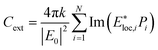 | (5) |
| |
 | (6) |
here * implies complex conjugate.
74 The scattering cross section is obtained from the following relation
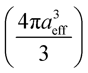
The extinction efficiency (Qext), absorption efficiency (Qabs), and scattering efficiency (Qsca) are obtained through the following set of equations
| |
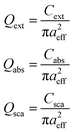 | (8) |
where
aeff is the effective radius of a sphere with volume

equal to the volume of the particle of any arbitrary shaped NP.
B. TDDFT method
For the calculation of excitation energy of molecular clusters the unrestricted density functional formalism is adopted, which is implemented in the Amsterdam Density Functional (ADF) program.75,76 The ground states of all molecular clusters are studied within the Local Density Approximation (LDA)77 and Generalized Gradient Approximation (GGA).78 For the GGA, the Becke's exchange79 and Lee–Yang–Parr correlation80 functional (BLYP) is chosen. The double-ζ (DZ) and the triple-ζ with double polarization (TZ2P) Slater type basis sets are used for geometry optimization. To check the vibrational stability of the clusters, all the frequencies and normal modes are calculated using both of the prior mentioned approximations (LDA and GGA). To calculate the excitation energy within frozen core condition, LB94 (ref. 81) is employed as exchange and B3LYP82 as correlation functional. The basis sets employed is similar to that used in geometry optimization process.
3. Results and discussion
A. DDA calculation
The calculations are performed for spherical, cubic and rod shaped Cu2O nanoparticles. In order to produce accurate result from DDA, the inter-dipole separation d should be made smaller than the structural length of the target.83 Hence, with the decrease in the target size; the dipole size is also reduced. Thus the typical cube size of each dipole is altered from 3.0 nm to 1.5 nm with subsequent variation in the number of dipoles (N) from 2.6 × 10⁵ to 4.5 × 10³. Though, polarizability αi depends on the refractive index of Cu2O;84 here the nanoparticles are assumed to be embedded in vacuum with refractive index one. The incident wavelength is varied from 150 nm to 750 nm.
Effect of size on absorption and scattering properties.
Cu2O nanospheres. The spherical Cu2O NPs are found to absorb in the UV region up to a limit of 80 nm in diameter, beyond which the absorption starts to occur at visible spectrum. Hence, the efficiency of absorption (Qabs), scattering (Qsca) and extinction (Qext) are calculated for Cu2O nanospheres ranging from diameter (D) 100 nm to 240 nm [Fig. 1(a)–(c)]. The absorbance is displayed within the wavelength region 150 nm to 750 nm. It is evident from the plots that decrease of the particle size causes blue shift of the peaks. A close inspection of the plots also reveals that with decrease in particle dimension there occurs a decrease in scattering and vis-à-vis increase in absorbance of the nanoparticles. As a consequence, the SPR peaks resemble to absorption and scattering peaks in smaller and larger dimensions respectively. This observation suits the relation displayed in eqn (7) and (8). The absorbance of the nanosphere of diameter 220 nm, obtained through DDA simulation is in well agreement with experimental value.85 This reinforces the accuracy of the DDA simulation, as is reported earlier.86 The molar absorption (εabs) and scattering (εsca) coefficients of nanospheres show a similar variation with size as that of equivalent cross sectional areas, which is in agreement with the proportionality between equivalent sectional area and the coefficients, εabs and εsca.87 The values of εabs and εsca in nanospheres, both measured at the same wavelength where SPR shows maximum efficiency, are reported in Table 1. The SPR maxima of nanospheres of diameters with 140 nm to 180 nm are close to the reported values (Table 1).88–90 With increase of size, the magnitude of visible light scattering (εsca) exhibits a steeper increase than εabs, which is attributed to the decrease of band gaps with increasing size of NPs. (Table 1 and Fig. 2). This observation is in qualitative agreement with the experimental findings for other semiconductors also.91 Here, the band gap (Eg) is estimated from the absorbance spectra,where, A is a frequency independent constant, hν is the energy of photons, n in the index depends upon the type of transition. For direct allowed band gap  .92 The calculated band gaps are close to the value of bulk band gap and the trend of variation of the band gap values also follow the literature.93 The spectra for efficiency of absorption shows two distinct peaks at larger dimension of the NPs. With the decrease in size, these two peaks approach each other and ultimately merge to a hump at a diameter of 120 nm (Fig. 1a).
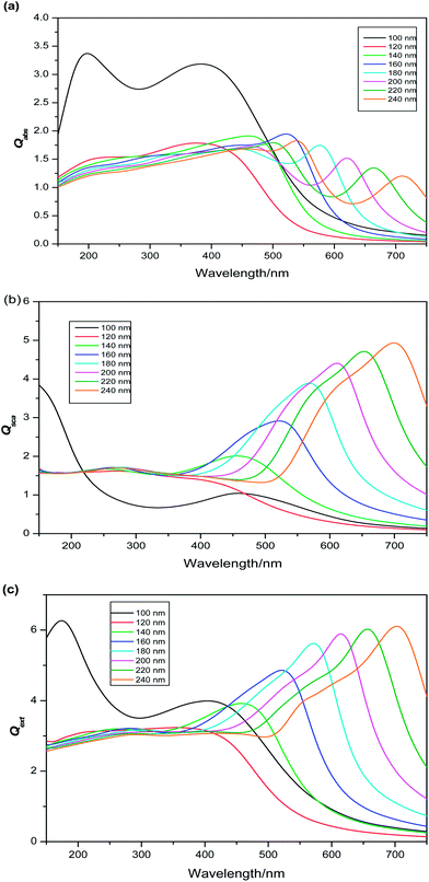 |
| | Fig. 1 Simulated spectra of (a) absorption (b) scattering and (c) extinction of Cu2O nanospheres with diameter 100 nm to 240 nm. | |
Table 1 Calculated molar absorption coefficients (εabs), molar scattering coefficient (εsca), surface area to volume ratio (S/V) and band gaps of NPs of varying shapes (sphere, cylinder, cube) and sizes at their corresponding surface plasmon resonance wavelength maximum (λmax)
| Shape |
Size nm |
λmax nm |
εabs × 1010 M−1 cm−1 |
εsca × 1010 M−1 cm−1 |
Band gap eV |
S/V (nm−1) |
| Sphere |
Diameter |
|
|
|
|
|
| |
100 |
404.7 |
6.46 |
1.75 |
2.32 |
0.06 |
| 120 |
386.87 |
5.31 |
4.36 |
2.48 |
0.05 |
| 140 |
459.79 |
4.37 |
8.1 |
2.29 |
0.043 |
| 160 |
522.83 |
10.2 |
15 |
2.17 |
0.037 |
| 180 |
576.56 |
11.6 |
26 |
2.03 |
0.033 |
| 200 |
622.03 |
12.5 |
36 |
1.7 |
0.03 |
| 220 |
663.32 |
13.4 |
47 |
1.65 |
0.027 |
| 240 |
711.46 |
14.4 |
58 |
1.64 |
0.025 |
| Cylinder |
Long axis |
Diameter |
Aspect ratio |
|
|
|
|
|
| 553 |
34 |
16.26 |
181 |
9.49 |
5.50 |
3.24 |
0.116 |
| 692 |
40 |
17.3 |
197 |
11.91 |
6.02 |
3.18 |
0.099 |
| 796 |
54 |
14.74 |
229 |
13.97 |
6.03 |
2.89 |
0.073 |
| 899 |
57 |
15.77 |
249 |
18.78 |
7.03 |
2.81 |
0.069 |
| 937 |
63 |
14.87 |
233 |
25.29 |
9.87 |
2.89 |
0.063 |
| 980 |
72 |
13.61 |
403 |
29.19 |
10.93 |
2.52 |
0.055 |
| 1145 |
77 |
14.87 |
427 |
38.88 |
13.26 |
2.49 |
0.052 |
| 1385 |
80 |
17.31 |
443 |
47.39 |
16.21 |
2.44 |
0.050 |
| Cube |
Diameter |
|
|
|
|
|
| 100 |
339.47 |
4.27 |
3.2 |
2.69 |
0.074 |
| 120 |
393.09 |
5.86 |
4.54 |
2.46 |
0.062 |
| 140 |
454.17 |
8.31 |
8.96 |
2.34 |
0.053 |
| 160 |
511.35 |
10.8 |
16.7 |
2.19 |
0.046 |
| 180 |
559.24 |
12.2 |
28.4 |
2.04 |
0.041 |
| 200 |
603.08 |
12.9 |
39.9 |
1.93 |
0.041 |
| 220 |
642.58 |
13.5 |
51.2 |
1.78 |
0.034 |
| 240 |
687.98 |
14.3 |
63.2 |
1.65 |
0.031 |
 |
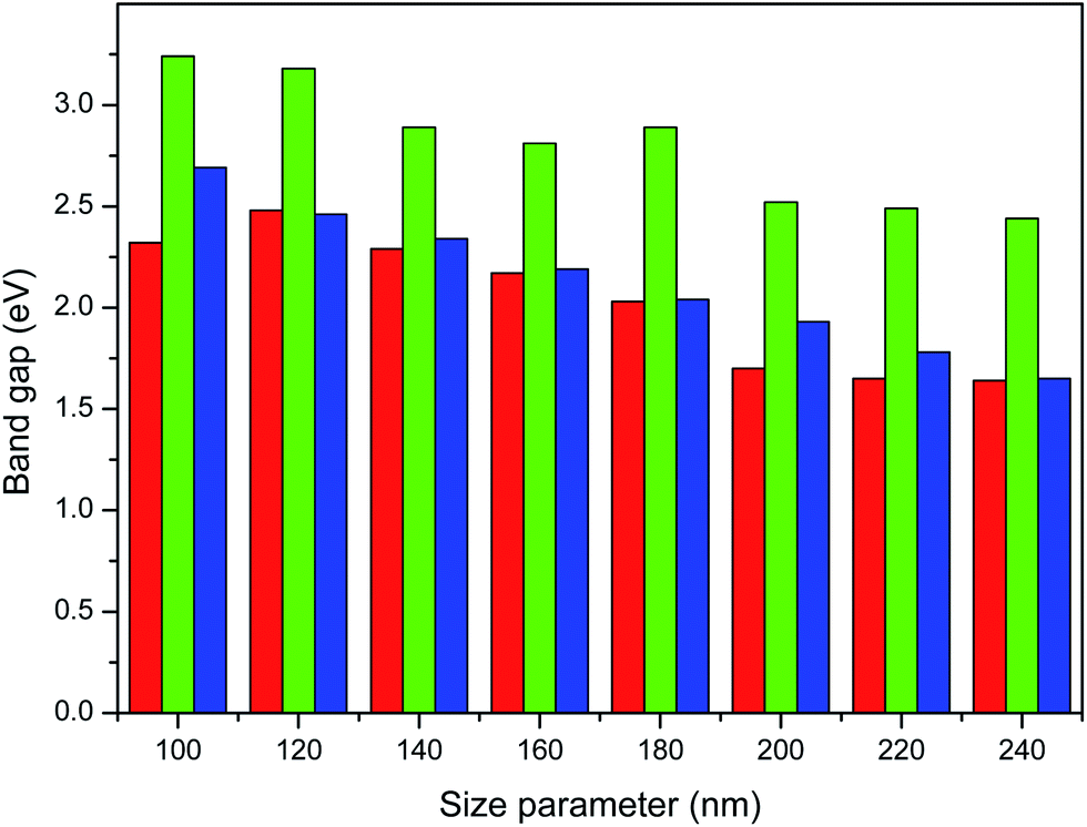
| | Fig. 2 Variation of calculated band gaps of spheres (red), cylinders (green) and cubes (blue) with increasing size parameters. | |
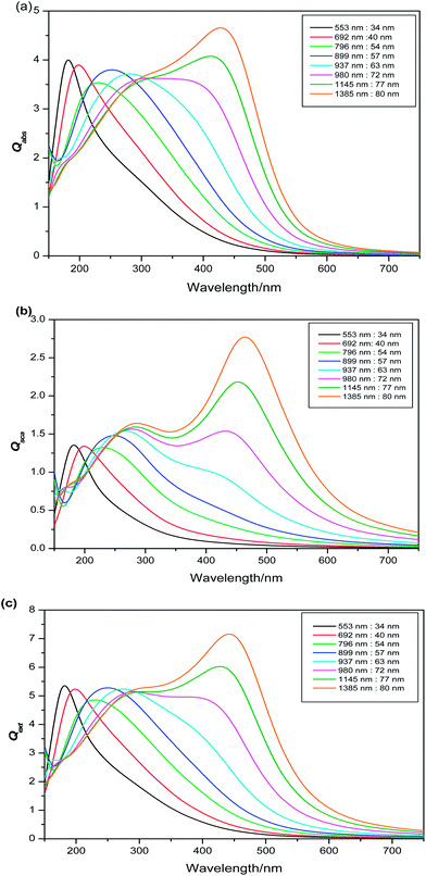 |
| | Fig. 3 Simulated spectra of (a) absorption (b) scattering (c) extinction of Cu2O nanocylinders with size parameters long axis![[thin space (1/6-em)]](https://www.rsc.org/images/entities/char_2009.gif) :diameter from 553 nm:30 nm to 1185 nm:80 nm. :diameter from 553 nm:30 nm to 1185 nm:80 nm. | |
 |
| | Fig. 4 Variation of absorption with shapes [sphere (red), cylinder (green), cube (black)] of NPs having equal volume of a sphere with effective radius 100 nm. | |
 |
| | Fig. 5 Variation of scattering with shapes [sphere(red), cylinder(green), cube(black)] of NPs having equal volume of sphere with effective radius 100 nm. | |
 |
| | Fig. 6 Simulated spectra of (a) absorption (b) scattering (c) extinction of Cu2O nanocubes having equal volume of nanospheres of diameter 100 nm to 240 nm. | |
Effect of symmetry on absorption and scattering properties. Usually the 3D shapes are represented by several descriptors, of which symmetry and surface area to volume ratio are maximally used. Symmetry is known as shape similarity descriptor and measures the similarity between two 3D shapes. Whereas, surface area to volume ratio (S/V) is termed as shape dissimilarity descriptor and measures the dissimilarity between two 3D shapes.95–99 Though, the dependence of absorption and scattering properties of the nano particle on the S/V ratio is well-cultivated;2,28,90–103 the same dependence on the symmetry needs a detail attention. According to nanothermodynamics,104 with increase of surface area the surface energy increases due to increment of density of elastic strain energy of lattice relaxation, density of dangling bonds and coordination imperfection. This enhancement of surface energy leads to the blue shift of band gap.105 According to chemical bond theory106,107 the optical gap shift (measured from the shift of absorption threshold of nanocrystal with respect to the bulk) appears from two types of effects. First is the quantum effect, responsible for quantum effect shift (ΔEkubo), which arises from the discretization of the band structure due to decrease in the dimension. Second is the surface effect, arising from termination of lattice periodicity on the surface of nanoclusters and responsible for surface effect shift (ΔEsurface). Thus, the energy gap shift (ΔE) can be represented as the sum of the two mentioned shifts (ΔE = ΔEkubo + ΔEsurface). The electronic structure, that defines the optical properties of NP is intimately related to the atomic structure and its symmetry. NPs with higher symmetry exhibit highly degenerate states. Reducing the symmetry split the degenerate MOs leads multiple energy states. Therefore tuning of symmetry affects the energy gap shift (ΔE) in nanoclusters.108 Since the S/V ratio of nanosphere and nanocube is comparable (Table 1), the distinction of absorption and scattering properties in those shapes is hardly correlated with surface effect shift (ΔEsurface) and symmetry becomes the chief reason behind the difference of their optical properties. To investigate this issue, the absorption and scattering efficiencies of Cu2O cluster of different symmetries are calculated keeping their size constant (D = 100 nm). The variation of scattering efficiency (Qsca) against different symmetries are shown in Fig. 5, which delineates highest efficiency for lowest symmetric cube. Hence, aligning with this order, minimum scattering efficiency should be displayed by most symmetric nanospheres. However, opposed to this trend, the cylinder shape is found to be associated with lowest Qsca and highest value of Qabs. This anomaly can be explained by the highest S/V ratio of cylinder compared to other shapes (Table 1). A considerable contribution from surface effect (ΔEsurface) also acts to enhance the value of ΔE in nanocylinder, for which the band gap becomes highest in case of nanocylinders. In a nutshell, the symmetry turns into an effective parameter to tune the band gap, which is in turn responsible for differentiation of optical response in nanoclusters.
B. TDDFT calculation
GGA functionals are reported to produce reasonably well prediction of excitation behavior in transition metal complexes.109 This functional is also found to reproduce the experimentally reported structure as evident from Table S1 in the ESI.† Hence, we finalized the optimized structure of the GGA functional for further calculation. A complete list of harmonic frequencies is given in the electronic (ESI†) for the optimized structures considered in this work. (Cu2O3)3 cluster with different symmetries imaginary frequencies of magnitude less than 31 cm−1 are found. This is reported to be likely due to small inaccuracy in the numerical grid.110
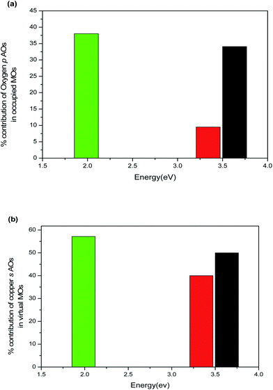
Effect of size. The TDDFT is exercised to obtain the excitation energy of (Cu2O)1, (Cu2O)2 and (Cu2O)3 clusters in their C2v symmetry (Fig. 7). The structural parameters in the optimized geometries of (Cu2O)n clusters [n = 1, 2, and 3] are found to be in well agreement with the reported bond distance111,112 (Table S3 of electronic (ESI†)). Analysis of the structure of Cu2O molecular clusters reveals four different coordination environments for Cu and O atoms which are designated as CuCSA, CuCUS, OCSA, OCUS. Here, the CSA and CUS in the suffix imply coordinatively saturated and coordinatively unsaturated respectively following the notations of Soon et al.113 In bulk state, each O atom is surrounded by four tetrahedron Cu atoms and referred to as OCSA. On the other hand, the coordination number varies from two to three in OCUS, which are denoted by OCUS2 and OCUS3 respectively. Similarly, CuCSA and CuCUS denote copper with coordination number two and one respectively. The alteration in size of the cluster brings about the change in the coordination number of surface atoms, which in turn leads to the change in structural parameters in the clusters.114–116 Due to the change in coordination with increase of size (in C2v symmetry), the CuCSA–OCUS and CuCUS–OCUS bond lengths decrease and CuCSA–CuCSA bond lengths increase (Table S3†). As a consequence, the bond angle ∠CuCSA–OCUS–CuCSA linearly increases with size. The increase in the size of cluster increases the population of surface atoms. Due to unsaturated coordination number, the surface atoms show a greater tendency to participate in the electronic transition for having more valence electrons compared to the bulk atoms. Thus, the variation in electronic transitions taking place between occupied and virtual MOs in clusters of increasing size is attributed to the reduction in coordination number (Table 2). For simplicity, only the peaks with highest oscillator strength (OS) (designated as 1 in Fig. 8) are reported for each cluster. The excitation peaks are directly dependent on the energy gap between occupied and virtual MOs (ΔEocc–vir), which can be found from Fig. 8 and Table 2. To find out the MO and its component AOs participating in the electronic transition, the partial density of states (PDOS) of fragments is analysed in Table S1 of ESI.† From Table S1,† it is seen that the occupied MOs are dominated by p AOs of O fragments with minor contribution of d AOs of Cu fragments. On the other hand the virtual MOs are dominated by s and p AOs of Cu fragments. Again, (Cu2O)3 and (Cu2O)2 are found to have highest and lowest percentage contribution of oxygen p AO in their occupied MOs (Fig. 9a). Nevertheless, the OS of electronic transition also increases with increase in percentage contribution of s AOs of Cu fragments in virtual MOs (Table 2 and Fig. 9b). A marked effect of variation of coordination number on the nature of electronic excitation has been revealed from MO diagram analysis (Fig. 8). In (Cu2O)1 and (Cu2O)3 the peaks designated as 1 are basically produced from 5A1 to 5B1 and 14A1 to 13B2 transitions respectively (Table 2). Here, nA1, nA2, nB1 and nB2 represent the n-th SCF molecular orbitals as generated in ADF. A1, A2,… are the subspecies of irreducible representation internally used by ADF. The labels A, B and subscripts 1, 2 are associated with standard notations in literature.117 The source MOs (5A1 and 14A1) are dominated by pz AOs of O1CUS2 and O7CUS2 in (Cu2O)1 and (Cu2O)3 respectively (the number in the subscript such as 1 and 7 implies the atom number of the clusters depicted in Fig. 7). On the other hand, the destination MOs (5B1 and 13B2) are formed through major contributions from s AOs of Cu2CUS, Cu3CUS in (Cu2O)1 and s AOs of Cu8CUS, and Cu9CUS in (Cu2O)3 (Fig. 8b). No OCUS2 atom is present in (Cu2O)2. The peak 1 in case of (Cu2O)2 is associated with transition from 10B2 to 17A1 MO. The 10B2 MO is composed of Cu2CUS, Cu3CUS dx2−y2 AOs and 17A1 MO is composed Cu2CUS, Cu3CUS s AOs. Hence from the above discussion it becomes apparent that the nature of electronic excitation is typically ligand to metal charge transfer (LMCT) in (Cu2O)1 and (Cu2O)3 and metal to metal charge transfer (MMCT) in (Cu2O)2. This observation is in concordance with XPS (X-ray photoelectron spectroscopy) study and other quantum chemical computations which concludes that charge transfer takes place in Cu2O from oxygen to copper.118 The peak 1 at 720 nm in case of (Cu2O)3 is found to be highest with full width at half maxima (FWHM) of 31.8 nm and that of (Cu2O)2 at 334 nm is lowest with FWHM of 13.6 nm among three sizes of the cluster (Fig. 8). Intensity of absorption is proportional to the product of square of OS and transition energy. The OS of peak 1 is lowest for (Cu2O)2 and highest for (Cu2O)3 while the OS of peak 1 of (Cu2O)1 with FWHM 7.28 nm is in between the two. Therefore intensity of absorption is lowest in case of (Cu2O)2 and highest for (Cu2O)3 (Fig. S1†). Hence, it can be expected that variation of absorption intensity basically depends on nature of electronic transition. The calculated values of Eexc of Cu2O quantum dots in Table 2 shows the similar trend of quantum size effect as reported in ref. 85 and thus validate the TDDFT results.
 |
| | Fig. 7 Molecular clusters of Cu2O (a) (Cu2O)1, (b) (Cu2O)2, (d) (Cu2O)3 in C2v symmetry, (c) and (e) are (Cu2O)3 in Cs and C3v symmetry respectively. | |
Table 2 Discrete electronic excitations of Cu2O clusters of different sizes in C2v symmetry calculated through TDDFT and compared with reported values in ref. 85
| Clusters |
Symmetry |
Peaks |
Occupied orbital |
Virtual orbital |
ΔEocc–vir (eV) |
Oscillator strength |
Excitation energy (eV) |
Reported excitation energy (eV) |
| (Cu2O)1 |
C2v |
1 |
5A1(HOMO − 2) |
5B1(LUMO + 1) |
3.42 |
0.095 |
3.90 |
3.54 (6.7 nm) |
| (Cu2O)2 |
C2v |
1 |
10B2(HOMO − 1) |
17A1(LUMO + 2) |
3.395 |
0.0822 |
3.69 |
2.76 (8 nm) |
| (Cu2O)3 |
C2v |
1 |
14A1(HOMO − 1) |
13B2(LUMO + 1) |
1.313 |
0.1923 |
1.72 |
2.63 (14 nm) |
 |
| | Fig. 8 (a) TDDFT valence excitation spectra (oscillator strength vs. excitation energy) of (Cu2O)1 (black), (Cu2O)2 (red) and (Cu2O)3 (green) clusters having same symmetry (C2v). Only the most intense discrete transitions are reported and labelled as 1. (b) The representation of MOs participating in the electronic transitions to form the most intense peaks labelled as 1 in (Cu2O)n clusters (n = 1, 2 and 3). x, y and z are the reference axis of the MOs. | |
 |
| | Fig. 9 Variation of extent of LMCT in terms of % contribution of (a) ligand AOs in occupied MOs and (b) metal AOs in virtual MOs in molecular clusters of (Cu2O)1(black), (Cu2O)2 (red) and (Cu2O)3 (green). | |
Effect of symmetry. In case of DDSCAT computation we have considered the effect of shape and associated symmetry of nanoparticles on the optical properties. During variation of symmetry the energy gap shift (ΔE) is predominantly regulated by ΔEkubo and ΔEsurface. To further verify how the interplay between ΔEkubo and ΔEsurface play a crucial role in tuning optical features, TDDFT is performed by varying the symmetry of (Cu2O)3 to Cs, C2v and C3v. Elevation of symmetry causes change in structural parameters due to variation in coordination numbers. The CuCSA–CuCSA bond length is shorter in C2v compared to the C3v geometry. Similarly the CuCSA–OCUS2 bond length descends from C2v to Cs. Consequently the relevant bond angles increases in higher symmetry, while the CuCSA–OCUS bond length remains approximately same in all the cases. The blue shift of Eexc of higher symmetry appears due to increase in ΔEocc−vir. For ease of analysis two types of peaks are chosen. Peak 1 corresponds to electronic transition of lowest excitation energy. The peaks are labelled as 1_Cs, 1_C2v and 1_C3v of their respective symmetries (Fig. 10a). The blue shift of peak 1 is attributed to ascending trend of ΔEocc–vir with increase of symmetry from Cs to C3v (Fig. 10a and Table 3). With the increase of symmetry degeneracy of energy levels increase. On the contrary reducing the symmetry split the degenerate levels to multiple states, which is attributed to the highest ΔEocc–vir value of C3v and lowest of Cs. The other type of peaks labelled as 2 are chosen on the basis of electronic transition with highest oscillator strength. The peaks are labelled as 2_Cs, 2_C2v and 2_C3v according to the symmetry with ascending order (Fig. 10a). The peak 2 for C2v symmetry (designated as 2_C2v) is found to be most intense than the other peaks (designated as 2_Cs and 2_C3v). The proper reason behind the variation of OS can be explored by analysis of PDOS data and MO diagram (Table S2† and Fig. 10b). The peak 2_C2v is generated due to the transition from 14A1 to 13B2 (vide supra) whereas, peak 2_Cs and 2_C3v are associated with transition from MO 20AAA to MO 22AAA and MO 95A to MO 100A. The transition from 14A1 to 13B2 in 2_C2v is purely LMCT type; whereas transition of 20AAA to 22AAA and 95A to 100A contains approximately equal d AOs contribution in 2_Cs and 2_C3v respectively (Table S3 in ESI†). Therefore oscillator strength varies linearly with extent of LMCT type transition. A remarkable agreement of the calculated values of Eexc of two different symmetries having approximately similar size (nanocubes and nanosphere) with reported results119,120 confirms the reliability of TDDFT computation (Table 3).
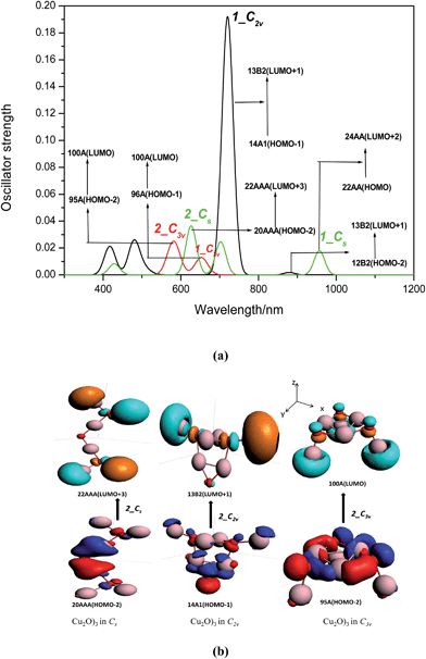 |
| | Fig. 10 (a) TDDFT valence excitation spectra (oscillator strength vs. excitation energy) of (Cu2O)3 clusters having different symmetries C2v (red) and D3h (black). The transitions with lowest excitation energy are reported as 1_Cs, 1_C2v, 1_C3v. The most intense discrete transitions are labelled as 2_Cs, 2_C2v and 2_C3v for respective symmetries. The MOs involved in corresponding transitions are also displayed. (b). The representation of MOs participating in the electronic transitions to form the most intense peaks labelled as 2_Cs, 2_C2v, 2_C3v for respective symmetries of (Cu2O)3 cluster. x, y and z are the reference axis of the MOs. | |
Table 3 TDDFT data of discrete electronic excitations of Cu2O clusters of same sizes in different symmetries
| Clusters |
Symmetry |
Peaks |
Occupied orbital |
Virtual Orbital |
ΔEocc–vir (eV) |
Oscillator strength |
Excitation energy (eV) |
Reported excitation energy (eV) |
| Is from ref. 119. Is from ref. 120. |
| (Cu2O)3 |
Cs |
1 |
22AA(HOMO) |
24AA(LUMO + 2) |
1.173 |
0.015 |
1.296 |
|
| 2 |
20AAA(HOMO − 2) |
22AAA(LUMO + 3) |
1.876 |
0.0302 |
1.98 |
|
| (Cu2O)3 |
C2v |
1 |
12B2(HOMO − 2) |
13B2(LUMO + 1) |
1.337 |
0.0018 |
1.409 |
2.36a (420 nm) |
| 2 |
14A1(HOMO − 1) |
13B2(LUMO + 1) |
1.313 |
0.1923 |
1.72 |
2.407a |
| (Cu2O)3 |
C3v |
1 |
96A(HOMO − 1) |
100A(LUMO) |
1.804 |
0.0064 |
1.898 |
2.25b |
| 2 |
95A(HOMO − 2) |
100A(LUMO) |
2.017 |
0.0126 |
2.13 |
2.38b |
C. Interpreting optical absorption spectra of Cu2O NPs with TDDFT data
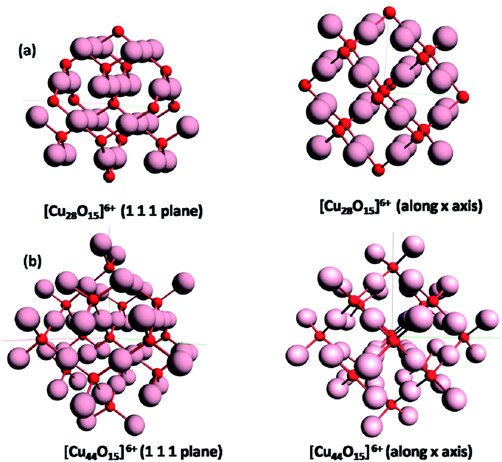
The analysis of electronic excitation of molecular clusters of (Cu2O)n clearly reveals that the variation in absorption spectra of NPs with different size and shape depends on two factors. The shifting of spectra (blue or red) takes place due to the variation of gaps between energy levels (ΔE). The measure of ΔE in case of NPs is ΔEkubo and in molecular cluster is ΔEocc−vir. The blue shift of spectra occurs when ΔE increases with decrease of size of nanoclusters. The second factor is the surface structure effect, which is dictated by the enhancement of ΔEsurface with increase of S/V ratio. This ΔEsurface contributes to the total energy gap (ΔE) and enhances the band gap value as well as absorption in NPs. The reason behind the increment of absorption can be rationalized by TDDFT results. The OS of excitation spectra predominantly depends on the nature of electronic transition among MOs. As it is suggested from earlier discussion, the nature of electronic transition depends on the structure of surface atoms. Two types of electronic transition takes place on Cu2O surface, LMCT and MMCT. Reduction in coordination number of O at the surface increases the p-orbital-density at the valence band compared to conduction band. Thus, the valence to unoccupied orbital transition is dominated by ligand to metal transition when the surface is oxygen terminated. On the other hand, the valence band will be dominated by d or s orbital of Cu if the surface is Cu terminated. This is clearly observed in the larger clusters calculation of [Cu28O15]6+ and [Cu44O15]6+(Fig. 11(a) and (b)). The peaks are blue shifted with decrease of size (Fig. 12(a) and (b)). This blue shift occurs due to increase of ΔEocc–vir (Table 4). This result shows a similar trend and similar kind of electronic excitation (Table S5 in ESI†) behavior as the smaller clusters which is easily observable from Fig. 12(a) and (b). In both of the larger clusters the AOs of core part do not take part in the excitation, which is in accordance with the results obtained for smaller clusters (Fig. S2 in ESI†). Enhancement of LMCT with lowering of cluster size can be attributed to the exposition of the O atoms to surface and thereby diminish their coordination environment. This is also observable from the simulated absorption spectra (Fig. 1a, 2a and 3a). Therefore, it can be concluded that the intensity of the peaks depend on the surface structure of nanoclusters. The peak intensity is influenced by LMCT if the surface is O-terminated and that of MMCT when the surface is Cu-terminated. Therefore, two types of peaks will arise, one of which is due to LMCT (OCUS2 to CuCUS) and another is due to MMCT (CuCSA to CuCUS). The peaks due to LMCT are found to appear in the lower energy region, while the higher energy region is dominated by peaks of MMCT type. Bruneval et al. who have explored from DOS and energy distribution curve (EDC) analysis that optical absorption spectra of Cu2O arises from two distinct energy levels; one between −8 and −5 eV which is typically O 2p level and the other within −5 eV to Fermi level recognized as the Cu d level.121 Therefore, the two distinct absorption peaks appearing in DDSCAT results is justifiable on the basis of the above observation.
 |
| | Fig. 11 Molecular clusters of (a) [Cu28O15]6+ and (b) [Cu44O30]6+ in Td symmetry. | |
 |
| | Fig. 12 TDDFT valence excitation spectra (oscillator strength vs. excitation energy) of (a) [Cu28O15]6+ and (b) [Cu44O30]6+ in Td symmetry. The most intense discrete transitions are labelled as peak_1. | |
Table 4 TDDFT data of discrete electronic excitations of larger Cu2O clusters of different sizes in same symmetry
| Clusters |
Symmetry |
Peaks |
Occupied orbital |
Virtual orbital |
ΔEocc–vir (eV) |
Oscillator strength |
Excitation energy (eV) |
| [Cu28O15]6+ |
Td |
1 |
71T2 |
38A1 |
2.157 |
0.00024 |
2.2 |
| 2 |
71T2 |
73T2 |
2.405 |
0.00011 |
2.4 |
| [Cu44O15]6+ |
Td |
1 |
19A1 |
43T2 |
1.198 |
0.116 |
1.514 |
| 2 |
19A1 |
44T2 |
1.567 |
0.0268 |
1.786 |
4. Conclusion
The present work unravels the effect of surface structure reconstruction and variation in band gap upon their surface plasmon resonance and associated electronic transition of Cu2O nanoparticles. The SPR peaks are found to be blue shifted with decrease in the size of the nanoparticles irrespective of the shapes, which is attributed to the increase of Kubo gap. This blue shift of SPR peak is also correlated with surface effect shift due to surface reconstruction during NP formation. As the shape of NP changes the related symmetry and S/V ratio also changes. Lowering of symmetry leads to splitting of degenerate energy levels. This is the reason behind the systematic change in optical response in between nanosphere and nanocube following the symmetry trend. The anomalous nature of optical response in case of cylinder can be explained from the enhancement of the band gap due to the inclusion of significant contribution of S/V ratio. The band gap varies linearly with S/V ratio as is apparent from Table 1. As a consequence the cylinder symmetry of Cu2O NPs are following completely different trend. Irrespective of diameter, the surface plasmon wavelength maximum (λmax) of the cylinder is completely blue shifted compared to sphere and cube. This is due to the largest band gap of the cylinders among the three shapes of same volume.
TDDFT computation is also performed to explore the phenomena of tuning optical response through surface structure reconstruction. The effect of size is traced by increasing the size of (Cu2O)n with n = 1, 2 and 3, keeping the C2v symmetry intact. On the other hand, the effect of symmetry on absorption is studied for a specific cluster (Cu2O)3 varying its symmetry from C2v to D3h. The energy gap between occupied and virtual MOs (ΔEocc–vir), increases with decrease of cluster size from (Cu2O)3 to (Cu2O)1. Increase of symmetry leads to the blue shift of peaks, which is realized due to a increase in ΔEocc–vir. The reconstruction of surface induces the variation in structural parameters due to change in coordination number of the surface atoms. The nature of electronic transition depends on the coordination number of surface atoms. On this account, two types of absorption occur on the surface of Cu2O NPs. As the coordination number of O atom decrease the absorption becomes LMCT type and with decrease of coordination number of Cu atoms the absorption becomes MMCT type. A similar result of the increase in the size of NP is also tested with clusters of larger and more realistic sizes. The results invariably show the same trend as is observed for smaller clusters. The blue shift in peaks with decrease in size is attributed to the increase of ΔEocc–vir. Therefore we can conclude that with change of size and symmetry the variation of two major factors play an important role to tune the absorption as well as surface plasmon resonance of Cu2O nanoclusters.
In the present work, it has been systematically shown that the optical property, i.e., SPR, absorption, and scattering can be tuned by manipulating size and symmetry of Cu2O nanostructures. Hence, these observations find sophisticated applications in the fields of biosensors, solar cells, photodiodes, photo catalysts etc.13–17 With the increment of size of Cu2O nanospheres the value of scattering coefficients become larger than the gold sphere, which is already employed for the selective imaging of cancer cells.122,123 The Cu2O nanospheres of D = 140 nm, 160 nm, 180 nm, 220 nm, and 240 nm have εsca greater than that of gold NPs. So these size ranges for Cu2O nanospheres can be used as cell imaging and detection of proteins as reported earlier.73 Therefore, this work can also guide the selection of appropriate size and shape of nanoclusters with desired band-gap for some specific application.
Acknowledgements
We sincerely thank the Department of Science and Technology, India, for financial support. TG thanks CSIR for senior research fellowship.
References
- S. M. Morton, D. W. Silverstein and L. Jensen, Chem. Rev., 2011, 111, 3962–3994 CrossRef CAS PubMed.
- C. Noguez, J. Phys. Chem. C, 2007, 111, 3806–3819 CAS.
- U. Kreibig and M. Völlmer, Optical Properties of Metal Clusters, Springer, Berlin, 1995 Search PubMed.
- M. L. Brongersma and P. G. Kik, Surface Plasmon Nanophotonics, Springer, Berlin, 1988 Search PubMed.
- S. A. Maier, Plasmonics, Springer, Berlin, 2006 Search PubMed.
- L. M. Liz-Marzán, Langmuir, 2006, 22, 32–41 CrossRef PubMed.
- A. Jakab, C. Rosman, Y. Khalavka, J. Becker, A. Trügler, U. Hohenester and C. Sönnichsen, ACS Nano, 2011, 5(9), 6880–6885 CrossRef CAS PubMed.
- C. Noguez and I. L. Garzón, Chem. Soc. Rev., 2009, 38, 757–771 RSC.
- G. Irmer, J. Monecke and P. Verma, Encyclopedia of Nanoscience and Nanotechnology, American Scientific Publishers, Los Angeles, California, USA 2003, vol. X, pp. 1–26 Search PubMed.
- A. P. Alivisatos, Science, 1996, 271, 933–937 CAS.
- M. A. Hines and P. Guyot-Sionnest, J. Phys. Chem., 1996, 100, 468–471 CrossRef CAS.
- B. O. Dabbousi, J. Rodriguez-Viejo, F. V. Mikulec, J. R. Heine, H. Mattoussi, R. Ober, K. F. Jensen and M. G. Bawendi, J. Phys. Chem. B, 1997, 101, 9463–9475 CrossRef CAS.
- W. P. Halparin, Rev. Mod. Phys., 1986, 58, 533 CrossRef.
- S. Link and M. A. El-Sayed, Annu. Rev. Phys. Chem., 2003, 54, 331 CrossRef CAS PubMed , PMID: 12626731.
- A. Kalsin, M. Fialkowski, M. Paszewski, S. K. Smoukov, K. J. M. Bishop and B. A. Grzybowski, Science, 2006, 312, 420 CrossRef CAS PubMed.
- D. A. Stuart, J. M. Yuen, N. Shah, O. Lyandres, C. R. Yonzon, M. R. Glucksberg, J. T. Walsh and P. V. Duyne, Anal. Cham., 2006, 78, 7211 CrossRef CAS PubMed.
- X. Huang, I. H. El-Sayed, W. Qian and M. A. El-Sayed, J. Am. Chem. Soc., 2006, 128, 2115 CrossRef CAS PubMed.
- E. Roduner, Chem. Soc. Rev., 2006, 35, 583–592 RSC.
- K. D. Sattler, Handbook of Nanophysics: Nanoparticles and Quantum Dots, CRC Press, United States of America, 2011 Search PubMed.
- K. S. Hamad, R. Roth, J. Rockenberger, T. Buuren and A. P. Alivisatos, Phys. Rev. Lett., 1999, 83, 17 CrossRef.
- L. Pizzagalli and G. Galli, Mater. Sci. Eng., B, 2002, 96, 86–89 CrossRef.
- F. Djurabekova and K. Nordlund, Phys. Rev. B: Condens. Matter Mater. Phys., 2008, 77, 115325 CrossRef.
- D. N. Pines, The Theory of Quantum Liquids, Addison-Wesley, New York, 1989 Search PubMed.
- A. L. Fetter and J. D. Walecka, Quantum Theory of Many-Particle Systems, McGraw-Hill, New York 1971 Search PubMed.
- J. M. Pitarke, V. M. Silkin, E. V. Chulkov and P. M. Echenique, Rep. Prog. Phys., 2007, 70, 1–87 CrossRef CAS.
- S. Asano and G. Yamamoto, Appl. Opt., 1980, 14, 29 CrossRef PubMed.
- A. C. Lind and J. M. Greenberg, J. Appl. Phys., 1966, 37, 3195 CrossRef PubMed.
- E. A. Coronado and G. C. Schatz, J. Chem. Phys., 2003, 119, 7 CrossRef PubMed.
- C. M. Anderson and K. P. Giapis, Phys. Rev. B: Condens. Matter Mater. Phys., 1997, 56, 12 CrossRef.
- M. E. Zoorob, M. D. B. Charlton, G. J. Parker, J. J. Baumberg and M. C. Netti, Mat. Sci. Eng., B, 2000, 74, 168–174 CrossRef.
- B. T. Draine and P. J. Flatau, J. Opt. Soc. Am. A, 1994, 11, 4 CrossRef.
- N. Félidj, J. Aubard and G. Lévi, J. Chem. Phys., 1999, 111, 3 CrossRef PubMed.
- M. A. Yurkin and A. G. Hoekstraa, J. Quant. Spectrosc. Radiat. Transfer, 2007, 106, 558–589 CrossRef CAS PubMed.
- A. Penttila, E. Zubko, K. Lumme, K. Muinonen, M. A. Yurkin, B. Draine, J. Rahola, A. G. Hoekstra and Y. Shkuratov, J. Quant. Spectrosc. Radiat. Transfer, 2007, 106, 417–436 CrossRef PubMed.
- F. Wang and T. Ziegler, Mol. Phys., 2004, 102, 23–24 CrossRef , 2585–2595.
- M. Seth and T. Ziegler, J. Chem. Phys., 2005, 123, 144105 CrossRef PubMed.
- N. Durante, A. Fortunelli, M. Broyer and M. Stener, J. Phys. Chem. C, 2011, 115, 6277–6282 CAS.
- C. M. Aikens, S. Li and G. C. Schatz, J. Phys. Chem. C, 2008, 112, 11272–11279 CAS.
- D. Snoke, J. P. Wolfe and A. Mysyrowicz, Phys. Rev. Lett., 1987, 59, 827–830 CrossRef CAS.
- D. Snoke, Science, 1996, 273, 1351–1352 CrossRef CAS.
- D. Snoke, Science, 2002, 298, 1368–1372 CrossRef CAS PubMed.
- A. Jolk and C. F. Klingshirn, Phys. Status Solidi B, 1998, 206, 841–850 CrossRef CAS.
- H. Matsumoto, K. Saito, M. Hasuo, S. Kono and N. Nagasawa, Solid State Commun., 1996, 97, 125–129 CrossRef CAS.
- A. Ettema and J. Versluis, Phys. Rev. B: Condens. Matter Mater. Phys., 2003, 68, 235101 CrossRef.
- K. Karpinska, M. Mostovoy, M. A. van der Vegte, A. Revcolevschi and P. H. M. van Loosdrecht, Phys. Rev. B: Condens. Matter Mater. Phys., 2005, 72, 155201 CrossRef.
- C. H. B. Ng and W. Y. Fan, J. Phys. Chem. B, 2006, 110, 20801 CrossRef CAS PubMed.
- J. Zhang, J. Liu, Q. Peng, X. Wang and Y. Li, Chem. Mater., 2006, 18, 867 CrossRef CAS.
- R. N. Briskman, Sol. Energy Mater. Sol. Cells, 1992, 27, 361–368 CrossRef CAS.
- A. O. Musa, T. Akomolafe and M. J. Carter, Sol. Energy Mater. Sol. Cells, 1998, 51, 305–316 CrossRef CAS.
- L. C. Olsen, F. W. Addis and W. Miller, Sol. Cells, 1982, 7, 247–279 CrossRef CAS.
- B. P. Rai, Sol. Cells, 1988, 25, 265–272 CrossRef CAS.
- P. E. de Jongh, D. Vanmaekelbergh and J. J. Kelly, Chem. Commun., 1999, 1069–1070 RSC.
- M. Hara, T. Kondo, M. Komoda, S. Ikeda, K. Shinohara, A. Tanaka, J. N. Kondo and K. Domen, Chem. Commun., 1998, 357–358 RSC.
- L. Xu, L. P. Jiang and J. J. Zhu, Nanotechnology, 2009, 20, 045605 CrossRef PubMed.
- L. Gou and C. J. Murphy, Nano Lett., 2003, 3, 231 CrossRef CAS.
- L. Gou and C. J. Murphy, J. Mater. Chem., 2004, 14, 735 RSC.
- D. Wang, M. Mo, D. Yu, L. Xu, F. Li and Y. Qian, Cryst. Growth Des., 2003, 3, 717 CAS.
- Z. Wang, X. Chen, J. Liu, M. Mo, L. Yang and Y. Qian, Solid State Commun., 2004, 130, 585 CrossRef CAS PubMed.
- M. J. Siegfried and K. S. Choi, J. Am. Chem. Soc., 2006, 128, 10356 CrossRef CAS PubMed.
- D. P. Singh, N. R. Neti, A. S. K. Sinha and O. N. Srivastava, J. Phys. Chem. C, 2007, 111, 1638 CAS.
- H. Xu, W. W. Wang and W. Zhu, J. Phys. Chem. B, 2006, 110, 13829 CrossRef CAS PubMed.
- M. J. Siegfried and K. S. Choi, Adv. Mater., 2004, 16, 1743 CrossRef CAS.
- H. Li, R. Liu, R. Zhao, Y. Zheng, W. Chen and Z. Xu, Cryst. Growth Des., 2006, 6, 2795 CAS.
- S. Jiao, L. Xu, K. Jiang and D. Xu, Adv. Mater., 2006, 18, 1174 CrossRef CAS.
- C. Lu, L. Qi, J. Yang, X. Wang, D. Zhang, J. Xie and J. Ma, Adv. Mater., 2005, 17, 2562 CrossRef CAS.
- J. J. Teo, Y. Chang and H. C. Zeng, Langmuir, 2006, 22, 7369 CrossRef CAS PubMed.
- Y. Chang, J. J. Teo and H. C. Zeng, Langmuir, 2005, 21, 1074 CrossRef CAS PubMed.
- W. Wang, G. Wang, X. Wang, Y. Zhan, Y. Liu and C. Zheng, Adv. Mater., 2002, 14, 67 CrossRef CAS.
- M. J. Siegfried and K. S. Choi, Angew. Chem., Int. Ed., 2005, 44, 3218 CrossRef CAS PubMed.
- Y. Chang and H. C. Zeng, Cryst. Growth Des., 2004, 4, 273 CAS.
- J. H. Jung, T. W. Kim, M. S. Song, Y. H. Kim and K. H. Yoo, J. Appl. Phys., 2007, 101, 093708 CrossRef PubMed.
- B. Balamurugan and B. R. Metha, Thin Solid Films, 2001, 396, 90–96 CrossRef CAS.
- W. J. Qi, C. Z. Huanga and L. Q. Chen, Talanta, 2010, 80, 1400–1405 CrossRef CAS PubMed.
- M. A. Yurkin and A. G. Hockstra, J. Quant. Spectrosc. Radiat. Transfer., 2007, 106, 558–589 CrossRef CAS PubMed.
- E. J Baerends, D. E. Ellis and P. Ros, Chem. Phys., 1973, 2, 41 CrossRef.
- C. F. Guerra, J. G. Snijders, G. Velde and E. J. Baerends, Theor. Chem. Acc., 1998, 99, 391 CAS.
- S. H. Vosko, L. Wilk and M. Nusair, Can. J. Phys., 1980, 58, 1200 CrossRef CAS PubMed.
- A. Cohen, Chem. Phys. Lett., 2000, 316, 160–166 CrossRef CAS.
- A. D. Becke, Phys. Rev. A: At., Mol., Opt. Phys., 1988, 38, 3098 CrossRef CAS.
- C. Lee, W. Tang and R. G. Parr, Phys. Rev. B: Condens. Matter Mater. Phys., 1988, 37, 785 CrossRef CAS.
- R. V. Leeuwen and E. Baerends, J. Phys. Rev. A, 1994, 49, 2421 CrossRef.
- P. J. Stephens, F. J. Devlin, C. F. Chablowski and M. J. Frisch, J. Phys. Chem., 1994, 98, 11623 CrossRef CAS.
- B. T. Draine and P. J. Flatau, User Guide for the Discrete Dipole Approximation Code DDSCAT 7.1, 2010, http://arxiv.org/abs/1002.1505 Search PubMed.
- E. D. Palik, Handbook of Optical Constants of Solids, Academic Press, Boston, 1985 Search PubMed.
- J. Zhang, J. Liu, Q. Peng, X. Wang and Y. Li, Chem. Mater., 2006, 18, 867–871 CrossRef CAS.
- C. Salzemann, A. Brioude and M.-P. Pileni, J. Phys. Chem. B, 2006, 110, 7208–7212 CrossRef CAS PubMed.
- P. K. Jain, K. S. Lee, I. H. El-Sayed and M. A. El-Sayed, J. Phys. Chem. B, 2006, 110, 7238–7248 CrossRef CAS PubMed.
- L. Zhang, H. Jing, G. Boisvert, J. Z. He and H. Wang, ACS Nano, 2012, 6, 3514–3527 CrossRef CAS PubMed.
- L. Zhang, D. A. Blom and H. Wang, Chem. Mater., 2011, 23, 4587–4598 CrossRef CAS.
- L. Zhang and H. Wang, ACS Nano, 2011, 5, 3257–3267 CrossRef CAS PubMed.
- C. S. Cheng, M. Serizawa, H. Sakata and T. Hirayama, Mater. Chem. Phys., 1998, 53, 225 CrossRef CAS.
- E. Rosencher and B. Vinter, Optoelectronics, Cambridge University Press, Cambridge, 2002 Search PubMed.
- D. Y. Liu, S. Y. Ding, H. X. Lin, B. J. Liu, Z. Z. Ye, F. R. Fan, B. Ren and Z. Q. Tian, J. Phys. Chem. C, 2012, 116, 4477–4483 CAS.
- L. Guan, H. Pang, J. Wang, Q. Lu, J. Yinac and F. Gao, Chem. Commun., 2010, 46, 7022–7024 RSC.
- N. Iyer, S. Jayanti, K. Lou, Y. Kalyanaraman and K. Ramani, Comput. Aided Des., 2005, 37, 509–530 CrossRef PubMed.
- M. A. Kassimi and O. El beqqali, International Journal of Computer Science Issues, 2011, 8, 3 Search PubMed.
- M. Kazhdan, B. Chazelle, D. Dobkin, A. F. Stein, T. A. Funkhouser, Reflective symmetry descriptor ECCV 2002, vol. 642, p. 656 Search PubMed.
- M. Kazhdan, B. Chazelle, D. Dobkin, T. Funkhouser, S. A. Rusinkiewicz, Reflective symmetry descriptor for 3d models. Algorithmica: Special Issue 2004 Search PubMed.
- P. Papadakis, I. Pratikakis, T. Theoharis and S. Perantonis, Int. J. Comput. Vis, 2010, 89, 177 CrossRef.
- C. Bauer, J.-P. Abid, D. Fermin and H. H. Girault, J. Chem. Phys., 2004, 120, 19 Search PubMed.
- J. Requejo-Isidro, R. Coso, J. Solis, J. Gonzalo and C. N. Afonso, Appl. Phys. Lett., 2005, 86, 193104 CrossRef PubMed.
- M. A. K. Abdelhalim, M. M. Mady and M. M. Ghannam, J. Nanomed. Nanotechnol., 2012, 3, 3 Search PubMed.
- C. Burda and M. A. El-Sayed, Pure Appl. Chem., 2000, 72, 1–331 CrossRef.
- G. Ouyang, X. L. Li, X. Tan and G. W. Yang, Appl. Phys. Lett., 2006, 89, 031904 CrossRef PubMed.
- G. Ouyang, A. Zhang, Z. Zhu, W. Zhu and G. Yang, J. Appl. Phys., 2011, 110, 033507 CrossRef PubMed.
- F. Gao, Inorg. Chem., 2010, 49, 10409–10414 CrossRef CAS PubMed.
- F. Gao, Appl. Phys. Lett., 2011, 98, 193105 CrossRef PubMed.
- H. Häkkinen, M. Moseler, O. Kostko, N. Morgner, M. A. Hoffmann and B. v. Issendorff, Phys. Rev. Lett., 2004, 93, 9 CrossRef.
- A. Rosa, G. Ricciardi, O. Gritsenko and E. J. Baerends, Struct. Bonding, 2004, 112, 49–116 CrossRef CAS.
- L. Zhao, L. Jensen and G. C. Schatz, J. Am. Chem. Soc., 2006, 128, 2911–2919 CrossRef CAS PubMed.
- M. Jadraque and M. Martin, Chem. Phys. Lett., 2008, 456, 51–54 CrossRef CAS PubMed.
- L.-S. Wang, H. Wu and S. R. Desai, Phys. Rev. B: Condens. Matter Mater. Phys., 1996, 53, 12 CrossRef.
- A. Soon, M. Todorova, B. Delley and C. Stampfl, Phys. Rev. B: Condens. Matter Mater. Phys., 2007, 75, 125420 CrossRef.
- D. Le, S. Stolbov and T. S. Rahman, Surf. Sci., 2009, 603, 1637–1645 CrossRef CAS PubMed.
- M. M. Islam, B. Diawara, V. Maurice and P. Marcus, THEOCHEM, 2009, 903, 41–48 CrossRef CAS PubMed.
- M. Altarawneh, M. W. Radny, P. V. Smith, J. C. Mackie, E. M. Kennedy, B. Z. Dlugogorski, A. Soon and C. Stampfl, J. Chem. Phys., 2009, 130, 184505 CrossRef PubMed.
- M. Ladd, Symmetry and Group Theory in Chemistry, Horwood Publishing, Chichester, 1998, pp. 89–91 Search PubMed.
- J. Morales, J. P. Espinos, A. Caballero and A. R. Gonzalez-Elipe, J. Phys. Chem. B, 2005, 109, 7758–7765 CrossRef CAS PubMed.
- K. Borgohain, N. Murase and S. Mahamuni, J. Appl. Phys., 2002, 92, 3 CrossRef PubMed.
- C.-H. Kuo, C.-H. Chen and M. H. Huang, Adv. Funct. Mater., 2007, 17, 3773–3780 CrossRef CAS.
- F. Bruneval, N. Vast, L. Reining, M. Izquierdo, F. Sirotti and N. Barrett, Phys. Rev. Lett., 2006, 97, 267601 CrossRef.
- K. Sokolov, M. Follen, J. Aaron, I. Pavlova, A. Malpica, R. Lotan and R. Richards-Kortum, Cancer Res., 2003, 63, 1999 CAS.
- I. H. El-Sayed, X. Huang and M. A. El-Sayed, Nano Lett., 2005, 5, 829 CrossRef CAS PubMed.
Footnote |
| † Electronic supplementary information (ESI) available: Optimised structural parameters and partial DOS (PDOS) data of Cu2O clusters with increasing size at C2v symmetry and of different symmetries at fixed size are given in tabulated form. TDDFT valence excitation spectra (intensity vs. wavelength) of (Cu2O)n (n = 1, 2 and 3) clusters having same symmetry (C2v) and of different symmetries are displayed. See DOI: 10.1039/c3ra45387a |
|
| This journal is © The Royal Society of Chemistry 2014 |
Click here to see how this site uses Cookies. View our privacy policy here. 
 are the amplitude and wave number of the incident wave respectively. The interaction matrix A can be represented as


 equal to the volume of the particle of any arbitrary shaped NP.
 .92 The calculated band gaps are close to the value of bulk band gap and the trend of variation of the band gap values also follow the literature.93 The spectra for efficiency of absorption shows two distinct peaks at larger dimension of the NPs. With the decrease in size, these two peaks approach each other and ultimately merge to a hump at a diameter of 120 nm (Fig. 1a).