DOI:
10.1039/C3RA45316B
(Communication)
RSC Adv., 2014,
4, 7476-7482
Hydrogen sensing based on nanoporous silica-embedded ultra dense ZnO nanobundles†
Received
24th September 2013
, Accepted 3rd January 2014
First published on 7th January 2014
Abstract
ZnO nanobundles were grown via a nano-templating technique over a porous silica bed using an aqueous chemical route. The growth of nanobundles initiated from ZnO nano-seeds positioned at various levels over a nanoporous matrix of self-assembled polymethylsilsesquioxane nanoparticles. Bundles of different features like nanowires, nanorods and nanotubes with a high surface roughness were grown over these templates by a day-long incubation in an aqueous solution of hexamethylene tetra-amine and zinc nitrate. We envisage these ZnO nanostructures for sensitive hydrogen detection. Photoluminescence spectra indicate the nanotubes to be most sensitive towards H2. We observe high reconditionability, moderate sensitivity and a temperature dependent charge carrier reversal phenomenon.
I. Introduction
Being a promising research material, ZnO nanostructures have been widely used in different applications like gas sensors, biosensors, visible light and UV sensors etc.1–6 Still, there is a colossal scope for new development in sensing aspects. Particularly important in this context are ways and means to develop highly reconditionable, high surface area, high aspect ratio ZnO structures with greater numbers of adsorption sites on their surface.1,2 Several complex fabrication techniques like physical vapor deposition,7,8 molecular beam epitaxy,9 sputtering methods,10 pulsed laser deposition methods,11 chemical methods etc. have been employed for obtaining these nanostructures. Among all these the aqueous chemical route is the most cost effective and simplest approach used to synthesize ZnO nanostructures. Some structures such as nanotubes,12–15 nanowires,16,17 nanorods,17 tetra pods,18 ribbons,19 nanopropellar,20 nanocombs21,22 etc. have been synthesized using this route. Aqueous chemical method of synthesizing ZnO nanostructures was developed by Vayssieres et al.23 wherein he observed the vertical structures by using the concentrations of precursors. Reactions in the process are usually driven by the minimization of the free energy of the system.24 Reason for the vertical growth of ZnO nanostructures has been explained on the basis of high energy polar surfaces of wurtzite crystals of ZnO containing alternating Zn2+ and O2− terminated surfaces.25,59 Although the vertical growth and associated enhancement of surface area has been explored by many researchers yet very few attempts have been made to realize high aspect ratio vertically standing nanostructures with different heights causing an extreme rough brush bed formulated at the nanoscale. Such a structure if realized would enhance the surface area many folds thereby creating additional sites and defects for sensing of gases. Furthermore, When a reducing gas such as hydrogen comes in contact with the nanostructures, Oxygen being most reactive gas in air participates in the reaction with the nanostructures by getting chemisorbed over the surface and creating O−1/O−2 state possibly by taking up all the free electrons, thereby realizing a potential barrier and reduction in conductivity which is shown in Fig. 1.
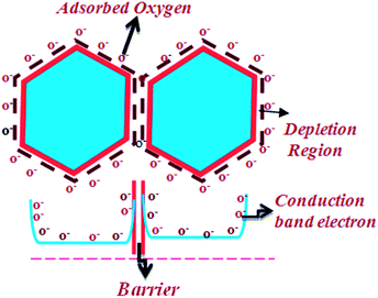 |
| | Fig. 1 Representation of the surface charge region over the surface and appearance of inter-grain contact resistance. | |
After reaction of H2 with ionosorbed oxygen, Electrons are given back to the bulk reducing the potential barrier and therefore increasing the conductivity. Bielanski et al. and Seiyama et al. have reported a change in the surface resistance upon such gas–solid interactions by looking at concentration effects of oxygen and cation vacancy on the gas sensing characteristics for nano-structured metal oxides.26,27 Most often, characteristics of gas sensing are correlated with band gap energy and defect concentration.28–31 Variegated nanostructures have been synthesized previously with wet chemical route and various other routes for sensitive gas detection.32–41 In order to address the surface area enhancement due to vertical growth of ZnO nanostructures at variable heights thereby achieving a highly rough brush bed configuration we have used a novel nano-templating technique (realized using the aqueous chemical route) which places ZnO nanoseeds at various levels along the cross-section of a high nanostructured PMSSQ nanoparticle self-assembly. Thorough characterization of the surface morphology of such structures with respect to the use of different combinations of precursors has been performed. These structures demonstrate novel aspects of sensing hydrogen gas like reconditionability of the films, a unique phenomenon of carrier reversal from n to p type, which has not been observed in ZnO utilized for hydrogen sensing prior to this as a function of the operating temperature.
II. Experimental section
A. Materials and methods
Three polymers namely PGMEA (propylene glycol methyl ether acetate, purchased from Sigma Aldrich) (CAS: 484431-4L) (empirical formula: C6H12O3), PPG (poly propylene glycol), (SARC CAQ 5322-69-4, (empirical formula: (CH(CH3)CH2O)n, molecular weight: 20![[thin space (1/6-em)]](https://www.rsc.org/images/entities/char_2009.gif) 000 g mol−1) and PMSSQ (SGR650F, Techmiglon) (empirical formula: (CH3SiO1.5)n) are mixed and the zinc oxide nanoseeds formulated using zinc acetate dehydrate (source: SDFCL, India) and isopropyl alcohol (source: SDFCL) are dispersed in the solution by using ultrasonication and vortexing methods. Silicon (100) p-type substrates (source: Logistic inc. NY) were thoroughly cleaned using AMD (acetone, methanol, de-ionized water) and 40% hydrofluoric acid (source: SDFCL, India) mixed in a 1:10 ratio with de-ionized water was used for passivating the silicon surface thereby resulting in a highly hydrophobic surface.42 A two step procedure was followed wherein the mixture of PMSSQ, PPG and nanoseeds in PGMEA was prepared as detailed later and spin coated on the treated silicon substrates as thin films of thicknesses up to 1.2 microns and was heated to achieve a porous template holding the embedded ZnO nanoseeds. The vertical structures were obtained on this template by holding the substrate upside down for 24 hours over a solution of zinc nitrate [Zn(NO3)2·6H2O] (source: Merck Specialties Pvt Ltd) and hexamethylenetetramine [C6H6N4] (source: Merck Specialties Pvt Ltd). The solution acted as a carrier of the zinc-oxide and transported this over the nanoseeds after passing through the pores and thus vertical nanostructures of zinc oxide of unequal heights were realized. The natural placement of the nanoseeds by the dispersion process was thoroughly characterized by performing elemental mapping on the films using a field emission scanning electron Microscope (FESEM) (Zeiss Supra 40V, Germany) and the morphology of the films with vertical nanostructure growing out was visualized using this setup. Further characterization of the nanostructures using X-ray diffraction (XRD) (Seift X-ray generator (ISO Debyeflex 2002, Germany)) with Cu-Kα source radiation (having wavelength 1.54 Å) for recording the vertical growth and also measurement of the built in stresses offered by the nano-template and a correlation to the oxygen defects using photoluminescence (Xenon Lamp Spectrofluorometer (Jobin Yvon, Fluorolog-3)) was successfully carried out on these vertical structures. Gas sensing trials were performed on these nanostructures using a dynamic measurement setup wherein hydrogen was varied up to concentrations 50–500 ppm and various aspects like sensitivity range, optimization of the operating temperature has been performed.
000 g mol−1) and PMSSQ (SGR650F, Techmiglon) (empirical formula: (CH3SiO1.5)n) are mixed and the zinc oxide nanoseeds formulated using zinc acetate dehydrate (source: SDFCL, India) and isopropyl alcohol (source: SDFCL) are dispersed in the solution by using ultrasonication and vortexing methods. Silicon (100) p-type substrates (source: Logistic inc. NY) were thoroughly cleaned using AMD (acetone, methanol, de-ionized water) and 40% hydrofluoric acid (source: SDFCL, India) mixed in a 1:10 ratio with de-ionized water was used for passivating the silicon surface thereby resulting in a highly hydrophobic surface.42 A two step procedure was followed wherein the mixture of PMSSQ, PPG and nanoseeds in PGMEA was prepared as detailed later and spin coated on the treated silicon substrates as thin films of thicknesses up to 1.2 microns and was heated to achieve a porous template holding the embedded ZnO nanoseeds. The vertical structures were obtained on this template by holding the substrate upside down for 24 hours over a solution of zinc nitrate [Zn(NO3)2·6H2O] (source: Merck Specialties Pvt Ltd) and hexamethylenetetramine [C6H6N4] (source: Merck Specialties Pvt Ltd). The solution acted as a carrier of the zinc-oxide and transported this over the nanoseeds after passing through the pores and thus vertical nanostructures of zinc oxide of unequal heights were realized. The natural placement of the nanoseeds by the dispersion process was thoroughly characterized by performing elemental mapping on the films using a field emission scanning electron Microscope (FESEM) (Zeiss Supra 40V, Germany) and the morphology of the films with vertical nanostructure growing out was visualized using this setup. Further characterization of the nanostructures using X-ray diffraction (XRD) (Seift X-ray generator (ISO Debyeflex 2002, Germany)) with Cu-Kα source radiation (having wavelength 1.54 Å) for recording the vertical growth and also measurement of the built in stresses offered by the nano-template and a correlation to the oxygen defects using photoluminescence (Xenon Lamp Spectrofluorometer (Jobin Yvon, Fluorolog-3)) was successfully carried out on these vertical structures. Gas sensing trials were performed on these nanostructures using a dynamic measurement setup wherein hydrogen was varied up to concentrations 50–500 ppm and various aspects like sensitivity range, optimization of the operating temperature has been performed.
B. Synthesis of zinc oxide nanoseeds
We started processing the nanostructures by synthesizing the nanoseeds separately by first using a well ultra-sonicated solution of zinc acetate dehydrate (concentrations varying from 0.005–0.025 M) in isopropyl alcohol (milky white in color) followed by filtration using 0.45 μm micro-syringe filters (source: Millipore) and applying the filtered solution in a drop wise, manner onto a pre-cleaned silicon substrate. Seeds of average size ∼5 nm got precipitated as the silicon substrate was heated to 200 °C and kept for a few seconds. The cycle was repeated five to six times to ensure the formation of a uniform nanoseed layer on the substrate surface. At 200 °C, the zinc acetate crystals decompose to formulate ZnO seeds.
Fig. 2 shows the representative scanning electron micrograph of such a seed coated silicon wafer using 0.01 M zinc acetate dehydrate. The layer deposited is then scrapped off the silicon surface using a sharp razor edge and collected in powder form in a vial. After accumulating sufficient weight of this powder their nanotemplating is performed as described below:
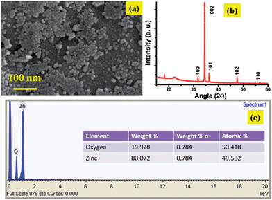 |
| | Fig. 2 (a) Scanning Electron Micrograph of zinc oxide seeds deposited over Si substrate. (b) XRD plot for seeded substrate shows that the seed exists in wurtzite crystal form with their c axis (002 plane). This orientation acts as an epitaxial site for the vertical growth of structures. (c) EDAX analysis confirms the zinc and oxygen presence. | |
C. Fabrication of nano-templated platform
Self-assembly of polymer nanoparticles due to their entropic and enthalpic interactions with another polymer medium in which these particles are dispersed result in highly self organized porous films. In this paper we have used the power of this self assembly for templating the placement of ZnO nanoseeds. The polymeric system used by us to achieve this task is a combination of PMSSQ nanoparticles and PPG all dissolved together with the nanoseeds formulated in the earlier step in a homogenous dispersion using PGMEA (solvent) in the following manner. PGMEA (5 g) is mixed separately with PMSSQ (5 g) and sonicated till a clear solution was obtained (solution 1). PGMEA (5 g) was mixed with PPG (5 g) (solution2). The powdered form of ZnO nanoseeds (0.1 g) as obtained in the last step were dispersed in solution 2 by ultrasonication resulting in an uniform coating of the PPG (surfactant) around the nanoseeds preventing their coagulation in solution.
UV-Vis spectroscopy of this solution was carried out to ascertain the size of the dissolved ZnO55 [ESI, S3†]. 3 g of the resulting solution was mixed with 7 g of solution-1 and again ultrasonicated for homogenous dispersion. Another silicon wafer (100) was cleaned using AMD protocol and hydrogen passivated by immersing it in 1:10 HF: DI water solution for 10 seconds. The solution prepared in the last step was immediately spin coated on this wafer at 3000 rpm for 30 seconds and the film obtained was ramped up to 450 °C in a hotplate and held at this temperature for 5 minutes. The film was thus heated above the decomposition temperature of PPG (>200 °C) caused the evaporation of PPG and entropic disturbances in the dispersed nanoparticles (both PMMSQ and ZnO) leading to random collisions between them and eventually particle–particle cross linking. The bonds thus formulated are ‘Si–O–Si’ and ‘Si–O–Zn’. FTIR spectra for these films [Fig. 3] reflect the presence of Zn–O–Si bond at wave number 939 per cm, Si–O–Si linkages at 1130 per cm, Zn–O stretching at 440 per cm.60 Fig. 4(a) shows a scanning electron micrograph of the highly nano-porous films with entrapped Zn–O nanoseeds. Fig. 4(b) shows the elemental mapping for zinc across the thickness of the films.
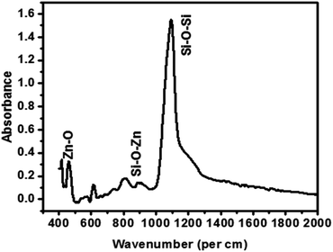 |
| | Fig. 3 FTIR spectra indicating the presence of various bond formulations in the film developed. | |
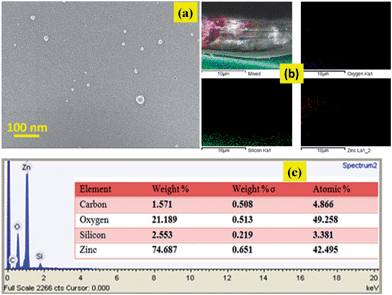 |
| | Fig. 4 (a) SEM image of the highly porous film with entrapped ZnO seeds, (b) elemental mapping clarifies the distribution of elements at various levels in the film matrix, (c) energy dispersive X-ray spectroscopy (EDAX) for chemical purity and percentage of the elements present in the film. | |
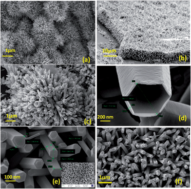 |
| | Fig. 5 FESEM images of ZnO nano structures, (a) and (b) at 0.01 M Zn(NO3)2; (c) and (d) at 0.005 M Zn(NO3)2 and (e) and (f) at 0.02 M Zn(NO3)2. | |
D. Fabrication of ZnO structures grown on the nanotemplate obtained in earlier step
For fabrication of the nanowires of ZnO, we use a mixture of zinc nitrate (Zn(NO3)2 and hexa methylene tetra amine (HMTA). This reaction is well explored by Green et al. (2006).44 The HMTA readily hydrolyses in water to slowly release formaldehyde (HCHO) and ammonia (NH3). The slow release of NH3 assists slow release of OH− thus enabling the minimization of bulk nucleation of Zn2+ in the solution; Further, the basic environment formed through the formation of OH− is needed for the formation of Zn(OH)2 which finally dehydrates to form ZnO under heated conditions. In our case, we consider three different [Zn2+]/HMTA ratios of 1:5, 2:5 and 0.5:5 (0.005 M: 0.05 M) maintained at neutral pH containing three immersed silicon wafers pre-coated with the nanoseeds containing templates (obtained in the last step) at temperature 90 °C in a gravity fed convection oven for 24 hours to grow nanowire, nanorod and nanotube structures over the nanotemplates respectively. Based on the reaction kinetics during this growth process the solution pH was regularly monitored and substrates were transferred into fresh solutions every time the precursor concentrations exhausted (reflected by a change in pH). Due to heated atmosphere ammonia formed bubbled out of the solution regularly and also the Zn2+ ions got exhausted,43–46 hence the replenishment of the precursors was necessary. The resultant structures formulated on the nanotemplate after this growth process of 24 hours were analyzed further for morphology using FESEM (Fig. 5a–f) and crystallographic orientation through X-ray diffraction (XRD) (Fig. 7) and room temperature photoluminescence (PL) (Fig. 6).
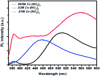 |
| | Fig. 6 Photoluminescence spectra for three different nano structures obtained at various concentration ratio of [Zn2+]/HMTA as 1:5, 2:5 and 0.5:5. | |
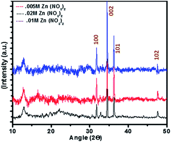 |
| | Fig. 7 XRD data plot for three different concentrations of zinc nitrate in the precursor solution. | |
Gas sensing setup controls the flow rates of the test and carrier gases and is able to maintain a desired gas concentration in the test chamber under a dynamic gas flow environment. There are three subunits in the setup, viz., a gas delivery unit, a reactor unit and a (resistance) measurement unit with temperature control [schematic provided as ESI, S1†]. The gas delivery line consists of a manifold, electro-magnetic/needle valves and mass flow controller unit to control the test gas concentration. The gas delivery system is designed to be dynamic in nature to make it realistic to the actual sensor development. The reactor unit has a temperature controlled thermal stage to heat the sensor material up to 375 °C and a Keithley 6517 A electrometer which are both controlled by a PC through RS 232 and GPIB interface using Lab view 8.5 (National Instruments). All measurements are performed at 1 V operating voltage at 1 Hz sampling frequency. Interdigitated electrodes needed for establishing electrical contacts on the brush bed is sputter deposited using a shadow mask wherein a thick layer of gold layer (∼1 μm) is sputter coated using the NSC400 sputtering system. (M/s Nano Master, USA). [Schematic representing the electrical connection of the film with electrodes is shown in ESI, S2†].
III. Results and discussions
A. Defect analysis
The nanoseeds produced as a result of decomposition of zinc acetate crystals are found to be in the size range of ∼9–10 nm. SEM images and the corresponding EDAX analysis of the structures are given in Fig. (4a–c). Analysis shows that the primary nanostructures are not exactly as per the stoichiometry and there are crystals defects present in them. A number of surface defects viz. Zn vacancies, interstitial oxygen, interstitial hydroxyl group or oxygen vacancies48 etc. can give rise to such defects. Wurtzite crystal lattice of ZnO reveals 60% of empty space47 which attracts the possibility of many surface defects. Synthesis carried out in closed oven cuts off the atmospheric oxygen supply, this together with the fact that ZnO growth was mainly carried out by condensation and dehydration reactions at the aggregates indicates the possibility of oxygen vacancies to be formed during synthesis. An analysis to confirm the type of defects is performed on morphologically variegated ZnO nanostructures prepared under different conditions.
Samples are given excitation wavelength 350 nm which is greater than the wavelength corresponding to the band gap energy of ZnO. All samples show two peaks which have been arisen at ∼500 nm which corresponds to (2.4 eV) broad green band and ∼370 nm which is attributed to near band edge transition. The green band emission is obtained from the radial recombination of photo generated hole with e− belonging to single ionized oxygen vacancy (Vo+) present on the surface50–54 and is observed when ZnO is fabricated under oxygen deficient condition.55 UV band emission at a room temperature can be featured to the radial quantum confinement effect of ZnO nano structures.56–58
Structures having 0.01 M Zn2+ have peak at ∼450 nm which corresponds to green band emission. For structures having 0.02 M Zn2+, the peak is shifted to right indicating the presence of more oxygen vacancies. Hollow structures (0.005 M Zn2+) do have largest peak corresponding to green emission. The greater the oxygen vacancy on the surface, the stronger would be the green band peak.56 So it can be interpreted that the hollow structures have more oxygen vacancies because of much higher surface area which can be better explanation to better gas sensing response. Further, Annealing of the zinc oxide films for oxygen defect confirmation was carried out with a heating rate 10° C min−1 in the presence of oxygen for 1 hour. The flow rate of oxygen was set to 300 sccm. An apparent blue shift in the annealed sample could be observed with the green emission peak shifting from 560 nm to ∼520 nm on annealing, which could be possibly due to corrections in crystal imperfections and lattice relaxations (Fig. 8). That can also be attributed to the decrease in number of oxygen interstitials with improvement of the structural order in ZnO nanowires upon annealing.
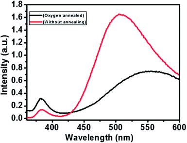 |
| | Fig. 8 PL spectra showing the comparison of ZnO nanowires with and without annealing. | |
B. Gas sensing investigation
Dynamic response of this sensor to different hydrogen gas concentration is shown in the Fig. 9. Changes in conductivity at temperatures less than 400 °C in the semiconducting oxide viz., SnO2, ZnO are commonly observed.49,61 Thus a critical step involved in the measurement scheme using the films of nanostructures is to ascertain the right temperature conditions for the optimum change in conductivity of the nanostructures. Once the operating temperature is determined the response and recovery time can be found for various gas concentrations. Sensitivity of the film is calculated by (Ra − Rg)/Ra × 100, where Ra is the resistance in air and Rg is the resistance of testing gas. These gas–sensor reactions normally take place at high temperatures (150–500 °C), providing the sensors to be internally heated for maximum response. The operating temperature must be optimized for the sensor material and the gas to be sensed.
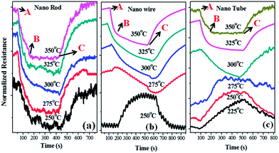 |
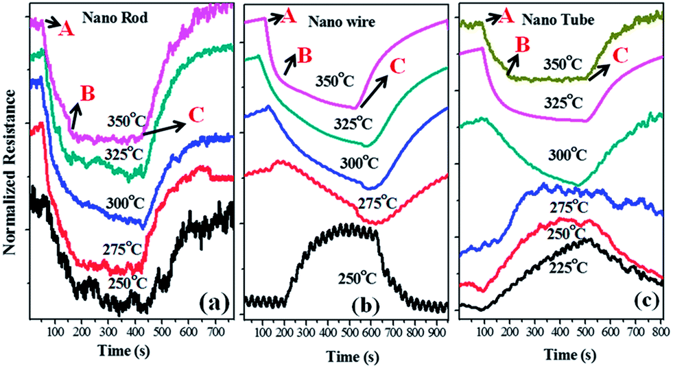
| | Fig. 9 Sensing plots for (a) nanorods, (b) nanowires and (c) nanotubes in which gas injection point, resistance saturation in gas atmosphere, gas supply off to bring back its original base resistance in air as point A, B and C respectively. | |
Fig. 9 shows the dynamic response of the nanowires, nanorods and nano-hollow tubes, at different ambient temperatures (varying from 225–350 °C). The hydrogen gas is cyclically injected into the testing chamber for around 7 minutes followed by its flushing out with normal air for an equal duration while the resistance of the film is measured real time. The normalized resistance is seen to decrease with gas injection at all temperatures (representative gas injection point shown as “A”, resistance saturation in gas atmosphere as “B” and gas supply off to bring back its original base resistance in air as “C” for 350 °C in Fig. 9. As can be observed from the resistance plots the sensing films recover its base resistance reasonably when the test gas is completely flushed out showing good reconditionability of the films. We observe a charge carrier reversal indicated by an increase in normalized resistance with gas injection in Fig. 9(b) at temperature 250 °C for the nanowire samples and in Fig. 9(c) at temperature 275 °C for the nanotube samples. Also, the prompt uplifting of the curve at point C in the graphs shows the higher time constant meaning thereby that the sensing can be performed with great rapidity.
Fig. 10 shows the plot for sensitivity variation with temperatures. The conductivity of a semi-conducting material can be represented by the following relation:
where
n and
p are the concentrations of electron and hole respectively,
q is the charge associated with the carrier and
μn and
μp are the mobility of electron and hole respectively.
61 The parameters
n,
p and their respective mobility are temperature dependent. For ZnO, the majority charge carriers are electrons, and minority carriers are hole. So a change in surface charge carrier may alter the overall conductivity by behaving n or p type in presence of gas. This phenomenon is observed by several authors due to several reasons like microstructure, operating temperature, humidity, gas concentration, doping,
etc. In the present report we have tuned the nanostructure for solid nano rod, thin rod or wire and highly porous nanotube. We have observed for nano rod sample that there is no carrier alteration in the entire temperature range (250–350 °C) and the material behaves as purely n type. However as the rod becomes thinner, a carrier alteration begins to occur at relatively low temperature 250 °C and this effect is more pronounced for hollow nano tube structure.
 |
| | Fig. 10 Sensitivity variation plot against temperature for (a) nanorods, (b) nanowires and (c) nanotubes. | |
The real mechanism of the observation lies in the fact that due to highly porous nature of one dimensional nanostructure, high surface area and very thin wall of the nanotube, the oxygen species can absorb on both inner and outer side of the nano tube (as depicting in Fig. 11) because larger amount of defect is produced inside/outside the wall which also can be observed from green emission of PL. When external oxygen molecules approach and chemisorb to sensor surface and replace the oxygen vacancies they thereby create large amount of holes. At this situation the concentration of holes is increased as the morphology is tuned from solid nano rod to porous nano tube.
where
V‥o is positive charge oxygen vacancies and h
˙ is the hole. The total carrier concentration, controlled by the space charge region, penetrates deeply into the ZnO nanotubes.
59,62–66 When the temperature is raised further the electron gets enough energy to reach conduction band and the concentration of electron is increased further thereby producing the n type conductivity at higher temperature for all types of nano structure. Sensitivity dependence on temperature is also presented in
Fig. 11. Although the sensitivity is high for nano rod sample at 325 °C. Porous nanotube structure at elevated temperatures gives significantly good sensitivity than the nanorod sample. Thus the change in morphology from rod to highly porous tube of ZnO can enhance the sensitivity compared to bulk and thin nanorod structure.
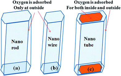 |
| | Fig. 11 Representation of oxygen adsorption over different nanostructures (a) nanorod (b) nanowire and (c) hollow nanotube. | |
IV. Conclusion
Another route has been investigated for the fabrication of high aspect ratio ZnO nanostructure having ultra high density. Sensing behavior has also been studied in dynamic condition where hydrogen gas response is tested. Because of the high surface area and gas diffusion towards whole surface area led to better gas response and adsorption–desorption phenomenon. Having observed the carrier transition in specific concentrations of zinc nitrate in the solution, behavior of these films can be altered to p or n type semiconductors by optimizing the operating temperature and concentration of reagents used. So, key role in enhanced gas sensing behavior is played by higher specific surface area structures which has enormous application in various other fields because of their higher surface energy.
Acknowledgements
Authors would like to thank the DST Unit on Soft Nanofabrication, I.I.T. Kanpur and the National Programme for Materials and Smart Structures (NPMASS) for providing financial support for this work.
References
- N. Yamazoe, Sens. Actuators, B, 1991, 5, 7–19 CrossRef CAS.
- E. Comini, C. Baratto, G. Faglia, M. Ferroni, A. Vomiero and G. Sberveglieri, Prog. Mater. Sci., 2009, 54, 1–67 CrossRef CAS PubMed.
- Y. Xi, C. G. Hu, X. Y. Han, Y. F. Xiong, P. X. Gao and G. B. Liu, Solid State Commun., 2007, 141, 506–509 CrossRef CAS PubMed.
- A. Manekkathodi, M. Lu, C. W. Wang and L. J. Chen, Adv. Mater., 2010, 22, 4059–4063 CrossRef CAS PubMed.
- S. Xu, Y. Ding, Y. G. Wei, H. Fang, Y. Shen, A. K. Sood, D. L. Polla and Z. L. Wang, J. Am. Chem. Soc., 2009, 131, 6670–6671 CrossRef CAS PubMed.
- A. Wei, X. W. Sun, J. X. Wang, Y. Lei, X. P. Cai, C. M. Li, Z. L. Dong and W. Huang, Appl. Phys. Lett., 2006, 89, 123902 CrossRef PubMed.
- Z. W. Pan, Z. R. Dai and Z. L. Wang, Science, 2001, 291, 1947–1949 CrossRef CAS PubMed.
- M. H. Huang, Y. Y. Wu, H. Feick, N. Tran, E. Weber and P. D. Yang, Adv. Mater., 2001, 13, 113–116 CrossRef CAS.
- Y. W. Heo, V. Varadarajan, M. Kaufman, K. Kim, D. P. Norton, F. Ren and P. H. Fleming, Appl. Phys. Lett., 2002, 81, 3046–3048 CrossRef CAS PubMed.
- T. W. Chiou, W. Y. Wu and J. M. Ting, Relat. Mater., 2003, 12, 1841–1844 CrossRef.
- Y. Sun, G. M. Fuge and M. N. R. Ashfold, Chem. Phys. Lett., 2004, 396, 21–26 CrossRef CAS PubMed.
- L. Vayssieres, K. Keis, A. Hagfeldt and S. E. Linquist, Chem. Mater., 2001, 13, 4395–4398 CrossRef CAS.
- H. D. Yu, Z. P. Zhang, M. Y. Han, X. T. Hao and F. R. Zhu, J. Am. Chem. Soc., 2005, 127, 2378–2379 CrossRef CAS PubMed.
- L. F. Xu, Q. Liao, J. P. Zhang, X. C. Ai and D. S. Xu, J. Phys. Chem. C, 2007, 111, 4549–4552 CAS.
- G. W. She, X. H. Zhang, W. S. Shi, X. F. Jack, C. Chang, C. S. Lee, S. T. Lee and C. H. Liu, Appl. Phys. Lett., 2008, 92, 053111 CrossRef PubMed.
- M. H. Huang, S. Mao, H. Feick, H. G. Yan, Y. Y. Wu, H. Kind, E. Weber, R. Russo and P. D. Yang, Science, 2001, 292, 1897 CrossRef CAS PubMed.
- L. Vayssieres, Adv. Mater., 2003, 15, 464–466 CrossRef CAS.
- Y. Qiu and S. Yang, Adv. Funct. Mater., 2007, 17, 1345–1352 CrossRef CAS.
- X. Fan, M. L. Zhang, I. Shafiq, W. J. Zhang, C. S. Lee and S. T. Lee, Adv. Mater., 2009, 21, 2393–2396 CrossRef CAS.
- P. X. Gao and Z. L. Wang, Appl. Phys. Lett., 2004, 84, 2883–2885 CrossRef CAS PubMed.
- F. Xu, K. Yu, G. D. Li, Q. Li and Z. Q. Zhu, Nanotechnology, 2006, 17, 2855–2859 CrossRef CAS.
- Y. H. Zhang, X. B. Song, J. Zheng, H. H. Liu, X. G. Li and L. P. You, Nanotechnology, 2006, 17, 1916–2192 CrossRef CAS.
- L. Vayssieres, K. Keis, A. Hagfeldt and S.-E. Lindquist, Chem. Mater., 2001, 13, 12 CrossRef.
- S. Xu, Y. Shen, Y. Ding and Z. L. Wang, Adv. Funct. Mater., 2010, 20, 1493–1495 CrossRef CAS.
- P. W. Tasker, J. Phys. C: Solid State Phys., 1979, 12, 4977–4984 CrossRef CAS.
- A. Bielanski, J. Deren and J. Haber, Nature, 1957, 179, 668–669 CrossRef CAS.
- T. Seiyama, A. Kato, K. Fujiishi and M. Nagatani, Anal. Chem., 1962, 34, 1502–1503 CrossRef CAS.
- M. Batzill and U. Diebold, Phys. Chem. Chem. Phys., 2007, 9, 2307–2318 RSC.
- M. W. Ahn, K. S. Park, J. H. Heo, J. G. Park, D. W. Kim, K. J. Choi, J. H. Lee and S. H. Hong, Appl. Phys. Lett., 2008, 93, 263103 CrossRef PubMed.
- N. Han, L. Chai, Q. Wang, Y. Tian, P. Deng and Y. Chen, Sens. Actuators, B, 2010, 147, 525–530 CrossRef CAS PubMed.
- P. P. Sahay and R. K. Nath, Sens. Actuators, B, 2008, 133, 222–227 CrossRef CAS PubMed.
- A. M. Ruiz, A. Cornet, K. Shimanoe, J. R. Morante and N. Yamazoe, Sens. Actuators, B, 2005, 109, 7–12 CrossRef CAS PubMed.
- J. H. Lee, Sens. Actuators, B, 2009, 140, 319–336 CrossRef CAS PubMed.
- R. A. Gerlitza, K. D. Benkstein, D. L. Lahr, J. L. Hertz, C. B. Montgomery, J. E. Bonevich, S. Semancik and M. J. Tarlov, Sens. Actuators, B, 2009, 136, 257–264 CrossRef PubMed.
- B. Deb, S. Desai, G. U. Sumanasekera and M. K. Sunkara, Nanotechnology, 2007, 18, 285501 CrossRef.
- M. H. Seo, M. Yuasa, T. Kida, J. S. Huh, K. Shimanoe and N. Yamazoe, Sens. Actuators, B, 2009, 137, 513–520 CrossRef CAS PubMed.
- A. Kolmakov, D. O. Klenov, Y. Lilach, S. Stemmer and M. Moskovits, Nano Lett., 2005, 5, 667–673 CrossRef CAS PubMed.
- J. Huang and Q. Wan, Sensors, 2009, 9, 9903–9924 CrossRef PubMed.
- H. Zhang, J. Wu, C. Zhai, N. Du, X. Ma and D. Yang, Nanotechnology, 2007, 18, 455604 CrossRef.
- K. Galatsis, L. Cukrov, W. Wlodarski, P. McCormick, K. Kalantar-zadeh, E. Comini and G. berveglieri, Sens. Actuators, B, 2003, 93, 562–565 CrossRef CAS.
- A. Gurlo, N. Barson, A. Opera, M. Sahm, T. Sahm and U. Weimar, Appl. Phys. Lett., 2004, 85, 2280–2282 CrossRef CAS PubMed.
- V. Korampally, M. Yun, T. Rajagopalan, P. K. Dasgupta, K. Gangopadhyay and S. Gangopadhyay, Nanotechnology, 2009, 20, 425602 CrossRef PubMed.
- S. Xu and Z. L. Wang, Nano Res, 2011, 4(11), 1013–1098 CrossRef CAS.
- Lori E. Greene, Benjamin D. Yuhas, M. Law, D. Zitoun and P. Yang, Inorg. Chem., 2006, 45, 7535–7543 CrossRef CAS PubMed.
- M. Law, L. E. Greene, J. C. Johnson, R. Saykally and P. D. Yang, Nat. Mater., 2005, 4, 455–459 CrossRef CAS PubMed.
- M. Oner, J. Norwig, W. H. Meyer and G. Wegner, Chem. Mater., 1998, 10, 460–463 CrossRef.
- L. Bin and Z. H. Chun, J. Am. Chem. Soc., 2003, 125(15), 4430–4431 CrossRef PubMed.
- S. Tuzemen, G. Xiong, J. Wilkinson, B. Mischuck, K. B. Ucer and R. T. Williams, Physica B, 2001, 1197, 308–310 Search PubMed.
- N. Barsan and U. Weimer, J. Electroceram., 2001, 7, 143–167 CrossRef CAS.
- T. Andelman, Y. Gong, M. Polking, M. Yin, I. Kuskovsky, G. Neumark and S. O'Brien, J. Phys. Chem. B, 2005, 109, 14314–14318 CrossRef CAS PubMed.
- G. W. She, X. H. Zhang, W. S. Shi, X. Fan and J. C. Chang, Electrochem. Commun., 2007, 9, 2784–2788 CrossRef CAS PubMed.
- Y. Sun, D. Riley and M. N. R. Ashfold, J. Phys. Chem. B, 2006, 110, 15186–15192 CrossRef CAS PubMed.
- Y. C. Kong, D. P. Yu, B. Zhang, W. Fang and S. Q. Feng, Appl. Phys. Lett., 2001, 78, 407 CrossRef CAS PubMed.
- K. Vanheusden, W. L. Warren, C. H. Seager, D. K. Tallant, J. A. Voigt and B. E. Gnade, J. Appl. Phys., 1996, 79, 7983 CrossRef CAS PubMed.
- A. van Dijken, E. A. Meulenkamp, D. Vanmaekelbergh and A. Meijerink, J. Lumin., 2000, 90, 123 CrossRef CAS.
- S. C. Lyu, Y. Zhang, H. Ruh, H.-J. Lee, H.-W. Shim, E.-K. Suh and C. J. Lee, Chem. Phys. Lett., 2002, 363, 134 CrossRef CAS.
- D. Banerjee, J. Y. Lao, D. Z. Wang, J. Y. Huang and Z. F. Ren, Appl. Phys. Lett., 2003, 83, 10 Search PubMed.
- L. E. Greene, M. Law, J. Goldberger, F. Kim, J. C. Johnson, Y. Zhang, R. J. Saykally and P. Yang, Angew. Chem., Int. Ed., 2003, 42, 3031–3034 CrossRef CAS PubMed.
- J. X. Wang, X. W. Sun, Y. Yang and C. M. L. Wu, Nanotechnology, 2009, 20, 465501 CrossRef CAS PubMed.
- J. W. Soars, J. E. Whitten, D. W. Oblas and D. M. Steeves, Langmuir, 2008, 24, 371–374 CrossRef PubMed.
- A. Gupta, S. S. Pandey and S. Bhattacharya, AIP Conf. Proc., 2013, 1536, 291–292 CrossRef CAS PubMed.
- K. Mukherjee and S. B. Majumder, Sens. Actuators, B, 2013, 177, 55–63 CrossRef CAS PubMed.
- Y. Cheng, R. S. Yang, J. P. Zheng, Z. L. Wang and P. Xiong, Mater. Chem. Phys., 2012, 137(1), 372–380 CrossRef CAS PubMed.
- A. Gurlo and R. Riedel, Angew. Chem., Int. Ed., 2007, 46, 3826–384865 CrossRef CAS PubMed.
- L. L. Fields, J. P. Zheng, Y. Cheng and P. Xiong, Appl. Phys. Lett., 2006, 88(26), 263102 CrossRef PubMed.
- N. Barsan and U. Weimar, J. Electroceram., 2001, 7(3), 143–167 CrossRef CAS.
Footnote |
| † Electronic supplementary information (ESI) available. See DOI: 10.1039/c3ra45316b |
|
| This journal is © The Royal Society of Chemistry 2014 |
Click here to see how this site uses Cookies. View our privacy policy here.