Surface-enhanced Raman scattering substrate based on a Ag coated monolayer array of SiO2 spheres for organic dye detection

Ming-Chung Wu *a, Min-Ping Linb, Shih-Wen Chenc, Pei-Huan Leea, Jia-Han Lic and Wei-Fang Su*bd
aDepartment of Chemical and Materials Engineering, Chang Gung University, Taoyuan 333-02, Taiwan. E-mail: mingchungwu@mail.cgu.edu.tw
bInstitute of Polymer Science and Engineering, National Taiwan University, Taipei 106-17, Taiwan. E-mail: suwf@ntu.edu.tw
cDepartment of Engineering Science and Ocean Engineering, National Taiwan University, Taipei 106-17, Taiwan
dDepartment of Materials Science and Engineering, National Taiwan University, Taipei 106-17, Taiwan

Received 20th September 2013 , Accepted 5th December 2013

First published on 5th December 2013


Abstract

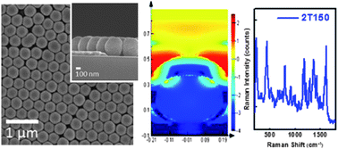
In this study, we developed a facile technique to fabricate a surface-enhanced Raman scattering (SERS) substrate. The technique involves self-assembling monodispersive SiO2 spheres on silicon wafer, then coating with a thin Ag film to form a SERS substrate comprised of a Ag coated monolayer array of SiO2 spheres. The substrate can detect minute amounts of organic dye. By optimizing the fabrication process, including controlling the size of the SiO2 spheres, the distribution of the SiO2 spheres on the silicon wafer, and the thickness of the Ag film, a dramatic increase in the enhancement of Raman scattering signals by surface plasmon resonance can be achieved. The enhancement of Raman scattering is closely correlated to the absorption peak of the organic dye and the excitation wavelength of the Raman system. A 40[thin space (1/6-em)]000-fold enhancement has been observed for a substrate prepared with 350 nm SiO2 spheres self-assembled on silicon wafer and coated with a 150 nm Ag layer. Through experimental and theoretical calculations (FDTD), such a strong signal intensity originates from the closeness between the absorption peak of the organic dye and the Raman excitation wavelength occurring at the hot spots of the SERS substrate. The high sensitivity, low cost and quick response provided by this type of SERS substrate are useful for the design and fabrication of functional devices and sensors.


Introduction

The technology for fabricating periodic metallic structures has been advanced rapidly due to the increased applications of surface-enhanced Raman scattering (SERS) spectroscopy in recent years.1–4 Conventional Raman spectroscopy is not sufficient to detect all matter, but impressive progress has been made in the development of surface-enhanced Raman scattering spectroscopy.5–10 The SERS spectroscopy technique has been developed as a fast and non-invasive analytical method for detecting environmental pollutants, bacteria, conducting polymers, metal oxides, etc.11–15 The SERS signal intensities are related to the size,16,17 shape,18–20 and distributions of the nanostructures.21–23 The SERS signals can be enhanced by a strong local electromagnetic field due to localized surface plasmon resonances (LSPR) coupled with the vibration intensities of the molecules near the nanostructures. Metallic nanostructures are usually used to study surface plasmon resonance and can be fabricated by lithography techniques, followed by thermal evaporation of a noble metal. However, some lithography techniques are time consuming and/or high cost, such as photolithography,24 focus ion beam etching,25 and electron beam lithography.26,27 Recent advances in colloidal lithography28,29 provide a number of advantages: firstly, the technique can form nanopatterns in a single step. Secondly, it is of a lower cost compared to the other expensive lithographic techniques. However, the metallic surface morphology fabricated by colloidal lithography has quite a complex surface plasmon resonance effect due to the superimposition of two gratings consisting of half-shells and truncated tetrahedra that are formed in the spaces between the spheres.30 Among the metals with the SERS effect, silver is an excellent candidate for use as a SERS substrate because the plasmon resonance frequency is usually within the visible region, and silver has an acceptable price.31,32

The fast and convenient detection of a dye or pigment in effluents has attracted great interest in recent years because the presence of dye in wastewater can inhibit sunlight penetration into watercourses and, therefore, reduce or even cease photosynthetic reactions in the aquatic environment. Moreover, some synthetic dyes are quite toxic, even carcinogenic, and harmful to people. As a result, developing a quick and easy method to detect dyes in solutions becomes important from both a scientific and environmental point of view.33

In this study, we developed a highly-sensitive and low-cost SERS substrate, consisting of a Ag coated monolayer array of SiO2 spheres synthesized by the self-assembly of the SiO2 spheres on Si, then followed by thermal evaporation of a thin Ag film. The fabricated SERS substrate was used to enhance Raman scattering signals of organic dyes, such as methyl red, methyl orange, brilliant green, and methylene blue. The light intensity distributions of different SERS structures were simulated using the finite-difference time-domain (FDTD) method. The surface plasmon resonance behavior of dye on the SERS substrate was investigated. The physical mechanisms of SERS were discussed based on both experimental observations and numerical studies. The results of this study provide a useful strategy to fabricate highly-sensitive and low-cost SERS substrates for detecting organic molecules.

Results and discussion

Various SERS substrates were prepared by spin coating monodispersive SiO2 spheres onto Si at different spin rates, followed by coating a thin Ag film on top of them. Samples prepared from 380 nm SiO2 spheres are denoted as xTyyy. The first letter x can be 1, 2, 3, 4, or 5 and indicates a spin rate of 1000, 2000, 3000, 4000 and 5000 rpm respectively. The second letter T means the thickness of Ag and the last three letters yyy represent the thickness of the Ag, which can be 50, 100, 150, 200 or 250 nm. The microstructures of the different SERS substrates were investigated using SEM. Fig. 1(a) shows a multilayer morphology of SiO2 spheres for the substrate prepared at a spin rate of 1000 rpm. When the spin rate is increased to 2000 rpm, the microstructure becomes a close packed layer of SiO2 spheres as shown in Fig. 1(b). Subsequently, the amount of SiO2 spheres on the substrate decreases on increasing the spin rate up to 5000 rpm as shown in Fig. 1(c)–(e). Furthermore, the electromagnetic coupling between two spheres causes extremely large Raman enhancements, and it is called the “hot-spot” effect. It has been reported that a large amount of “hot-spots” can be used as very powerful detection tool.34 Finally, we chose the SERS substrate prepared at the 2000 rpm spin rate for further study due to its large amount of hot spots and periodic structure. Fig. 1(f) shows the cross-sectional SEM image of the SERS substrate prepared at a 2000 rpm coating rate. A monolayer of SiO2 spheres can be clearly observed.
image file: c3ra45255g-f1.tif
Fig. 1 SEM images of various SERS substrates prepared by first spin coating 380 nm SiO2 spheres on Si at different spin rates, then coating them with 100 nm Ag, (a) 1000 rpm (Sample 1T100), (b) 2000 rpm (Sample 2T100), (c) 3000 rpm (Sample 3T100), (d) 4000 rpm (Sample 4T100), (e) 5000 rpm (Sample 5T100), (f) the cross section image of the 2T100 SERS substrate.

The morphologies of the different sized SiO2 spheres on the SERS substrate fabricated at a fixed spin rate of 2000 rpm were also evaluated using SEM. Fig. 2 shows that the SiO2 spheres can be self-assembled into a close packed monolayer. The sample prepared with 380 nm SiO2 spheres (Fig. 2(a)) shows the closest self-assembly packing when compared with the samples either prepared with the 425 nm (Fig. 2(b)) or 525 nm (Fig. 2(c)) SiO2 spheres. Although some defects still existed in the imperfect hexagonally-arranged SiO2 sphere film, the proportion of defects was less than 10% as shown in Fig. 2(a). The extinction spectra of the different SERS substrates prepared by the self-assembly of different sizes of SiO2 spheres on silicon wafer are shown in Fig. 2(d). The extinction spectra show a red shift of λmax from 625.0 nm to 780.0 nm and then to 879.2 nm with an increase in the size of the SiO2 spheres from 380 nm to 425 nm and to 525 nm, respectively. For the 2T100 SERS sample, λmax (625 nm) is the closest to the excitation wavelength of 632.8 nm. Thus, as the peak position of the surface plasmon resonance approaches the excitation laser wavelength of 632.8 nm, we are able to obtain a larger enhancement of the surface-enhanced Raman scattering. Additionally, the SEM images (Fig. 2(a)–(c)) indicate that the sample prepared with the 380 nm SiO2 spheres has the largest amount of hot spots among the three different sizes of SiO2 spheres.


image file: c3ra45255g-f2.tif
Fig. 2 SEM images of the different SERS substrates prepared by self-assembly of different sizes of SiO2 spheres on silicon wafer using spin coating, (a) 380 nm (Sample 2T100), (b) 425 nm, and (c) 525 nm. (d) The extinction spectra of various SERS substrates. The spin coating rate was fixed at 2000 rpm.

In order to confirm the effect of surface-enhanced Raman scattering on our SERS substrate, we selected several organic dyes as model compounds to coat our SERS substrate. Fig. 3(a)–(d) are Raman spectra of methyl red, methyl orange, brilliant green, and methylene blue on SERS substrates respectively. The substrates were prepared using different spin rates for spin coating the SiO2 spheres. They are arranged in vertical rows and labeled from 1 to 5 from bottom to top with increasing spin rates as shown in Fig. 3(a-1)–(a-5) to (d-1)–(d-5). Fig. 3 indicates that the substrate prepared at 2000 rpm exhibits the strongest Raman scattering signals. The Raman peak at 1388 cm−1 in the spectra of methyl red is the deformation vibration of the aromatic C–N bonds.35 The Raman peak at 1141 cm−1 in the spectra of methyl orange is the deformation vibration of the aromatic C–C bonds.36,37 The Raman peak at 441 cm−1 in the spectra of brilliant green is the deformation vibration of the conjugated aromatic C–C bonds.38 The peak at 484 cm−1 in the spectra of methylene blue is the deformation vibration of the C–N–C bonds.39 We chose the characteristic peak of each dye to calculate its enhancement factor (EF). The EF value is defined by dividing the intensity of the Raman characteristic peak of the organic dye on the SERS substrate by its intensity on a glass slide as shown below:27,40

 
EF = ISERS substrate/Iglass slide (1)


image file: c3ra45255g-f3.tif
Fig. 3 Raman spectra of four kinds of organic dyes, (a) methyl red, (b) methyl orange, (c) brilliant green, and (d) methylene blue, on various SERS substrates prepared from self-assembled SiO2 spheres at different spin rates, (ϒ-1 series) 1000 rpm (Sample 1T100), (ϒ-2 series) 2000 rpm (Sample 2T100), (ϒ-3 series) 3000 rpm (Sample 3T100), (ϒ-4 series) 4000 rpm (Sample 4T100), (ϒ-5 series) 5000 rpm (Sample 5T100).

The EF values of the 2T100 SERS substrate for methyl red, methyl orange, brilliant green, and methylene blue are 200, 700, 27[thin space (1/6-em)]000, and 1500, respectively. Brilliant green on the 2T100 SERS substrate results in the largest SERS enhancement factor (27[thin space (1/6-em)]000 times), because its absorption λmax of 625 nm is close to the wavelength of the He–Ne laser (Fig. 4). The photon energy of the surface plasmon resonance is close to that of the excitation so the strongest enhancement is observed. In order to calculate the EF value in our study, some literature reported that the difference between the number of adsorbed molecules on the SERS substrate and a flat glass surface needs to be considered due to the fact that the surface areas are different.41,42 However, using the spin coating process to deposit organic dyes on the SiO2 sphere substrates will cause movement or outflow of the SiO2 spheres. Hence, we used eqn (1) to calculate the EF value here.


image file: c3ra45255g-f4.tif
Fig. 4 Absorption spectra of methyl red, methyl orange, brilliant green, and methylene blue.

The thickness of the metal on the SERS substrate is a key parameter in determining the position of surface plasmon resonance. The SiO2/Si sample, prepared by the self-assembly of SiO2 spheres at 2000 rpm on Si, exhibits the largest amount of hot spots and was selected for further study. The SiO2/Si sample was coated with five different thicknesses of silver: 50 nm, 100 nm, 150 nm, 200 nm and 250 nm, to make SERS substrates. The surface morphologies of these SERS substrates were investigated by AFM. Fig. 5(a)–(f) show that the Z-range surface roughness decreases from 373.0 nm to 103.0 nm upon increasing the metal thickness from 0 nm to 250 nm. Table 1 summarizes the results.


image file: c3ra45255g-f5.tif
Fig. 5 The topographic images and cross-section profiles of (a) self-assembled SiO2 spheres on the Si sample (2T000) and 5 different SERS substrates coated with different metal thicknesses, (b) 2T050, (c) 2T100, (d) 2T150, (e) 2T200 and (f) 2T250.
Table 1 The Z-range and enhancement factor of various SERS substrates coated with different metal thicknesses
Sample Metal thickness (nm) Z-range (nm) Enhancement factor (times)
2T050 50.0 352.7 17[thin space (1/6-em)]700
2T100 100.0 317.1 27[thin space (1/6-em)]000
2T150 150.0 288.2 40[thin space (1/6-em)]000
2T200 200.0 123.4 34[thin space (1/6-em)]000
2T250 250.0 103.0 32[thin space (1/6-em)]000


From the AFM topographic images and SEM images, we speculate that the growth mechanism of the SERS hot spots stems from the process of Ag deposition on the sample of self-assembled SiO2 spheres on silicon (SiO2/Si). The deposition of Ag on SiO2/Si gradually fills the gap between the SiO2 spheres as depicted in Fig. 6. We estimate that the gap is about 50 nm before the Ag deposition. With the increasing Ag thickness, the gap decreases to approximately 30, and then 10 nm as shown in Fig. 6(a)–(c). The gap closes when the thickness of Ag is over 150 nm and a shallow ditch forms as a hot spot as shown in Fig. 6(d)–(f).


image file: c3ra45255g-f6.tif
Fig. 6 Schematic sketch of the growth mechanism of SERS hot spots as shown by the cross-section of various samples (a) without Ag (2T000), with different Ag thicknesses: (b) 2T050, (c) 2T100, (d) 2T150, (e) 2T200 and (f) 2T250.

The finite-difference time-domain (FDTD) method is adopted to verify our speculation. This method calculates the electric field intensity distribution in our ordered SERS substrates. In our simulation, a plane wave is set to illuminate from the top to the bottom, the perfectly matched layers are set on the top and bottom surfaces, and the periodic boundary conditions are set on the side walls. The results are presented in Fig. 7. The strong electric field enhancement occurs at the bottom of the spheres where the Ag shell and SiO2 interact and is induced by the narrow ditch between spheres. The emitted light penetrates the Ag through to the SiO2 when the deposited Ag shell is thin (≤100 nm) as shown in Fig. 7(a) and (b). When the thickness of Ag increases (>100 nm), the margin between two spheres causes the strong field enhancement to couple with SiO2 in Fig. 7(c) and (d). The sample covered with 150 nm Ag (2T150), exhibits the strongest field enhancement above the Ag surface. When the thickness of Ag is increased further, the granules of Ag become larger and the Ag surface becomes smoother. The sample with the 250 nm Ag coating (2T250) behaves like bulk silver with a rough surface and the emitted light can't reach the SiO2 as shown in Fig. 7(e). Though the enhanced field is as strong as those shown in Fig. 7(a) and (b), it concentrates in SiO2 or the bottom of the spheres where the dyes can't reach or the Raman signal can't be detected. Thus, the Raman intensities of 2T050 and 2T100 are smaller than the others and 2T150, 2T200 and 2T250 achieve stronger Raman intensities because the field enhancement concentrates on the Ag surface of the ditch. The Raman spectra of brilliant green on various SERS substrates with different metal thicknesses are shown in Fig. 8. The results are summarized in Table 1. Sample 2T150 has the strongest Raman intensity due to its groove between the SiO2 spheres being the narrowest among the five samples. The result is in agreement with the extremely high surface plasmon enhanced resonance electric field observed in gold bowtie nanoantenna.43 Our proposed growth mechanism of “hot spots” in the SERS substrates is confirmed both theoretically and experimentally. From Fig. 9, increasing the Ag thickness of the SERS substrates can lead to the red shift of the extinction peak due to the different extent of coupling between the SiO2 spheres and the Ag surface plasmon resonance. We can tune the surface plasmon resonance by adjusting the Ag thickness to coincide with the excitation wavelength of 632.8 nm. As a result of the likely efficient energy transfer from silver surface plasmons to brilliant green, 2T150 exhibited the strongest Raman intensity of up to 40[thin space (1/6-em)]000 because its λmax (634.5 nm) of the extinction spectra is close to that of the excitation. Thus, as the peak position of the surface plasmon resonance approaches the excitation laser wavelength of 632.8 nm, we are able to obtain a larger enhancement of the surface-enhanced Raman scattering. Therefore, the high sensitivity, low cost and quick response provided by this type of SERS are useful for the design and fabrication of functional devices and sensors.


image file: c3ra45255g-f7.tif
Fig. 7 The electric field distributions of SERS substrates with different Ag thicknesses of 50, 100, 150, 200, and 250 nm for samples (a) 2T050, (b) 2T100, (c) 2T150, (d) 2T200, and (e) 2T250, respectively. They are the electric field distributions in the cross section of a sphere at a wavelength of 633 nm. The scale is logarithmic. The distribution is calculated using the FDTD method.

image file: c3ra45255g-f8.tif
Fig. 8 Raman spectra of brilliant green on various SERS substrates with different Ag thicknesses, 50, 100, 150, 200 and 250 nm for samples 2T050, 2T100, 2T150, 2T200 and 2T250, respectively.

image file: c3ra45255g-f9.tif
Fig. 9 Extinction spectra of various SERS substrates with different Ag thicknesses, 0, 50, 100, 150, 200 and 250 nm for samples 2T000, 2T050, 2T100, 2T150, 2T200 and 2T250, respectively.

Experimental details

Synthesis of amorphous monodispersive SiO2 spheres

Amorphous monodispersive SiO2 spheres were synthesized by using a sol–gel method reported in the literature.44 20 ml of tetraethylorthosilicate (TEOS, 98%, Acros Organics) was dissolved in 200 ml ethanol (95%) and the solution was stirred at 30 °C for 30 min. Then, different amounts of ammonia solution (ammonium hydroxide, 28–30 wt% solution of NH3 in water) ranging from 20 to 40 ml were added to the TEOS solution and stirred for 2 h. After 2 h of the reaction, SiO2 spheres with different particle sizes, such as 380, 425 and 525 nm, were obtained. Then, the SiO2 colloid solutions were centrifuged at 5000 rpm for 10 min to separate the SiO2 spheres from the liquid. The SiO2 spheres were then washed using 200 ml ethanol accompanied with ultrasonication. The washing procedure was repeated three times to ensure the complete removal of reactants. Finally, the SiO2 spheres were dried at 100 °C for 12 h.

Fabrication of the surface-enhanced Raman scattering substrate of Ag coated SiO2 spheres on Si

2.0 wt% of amorphous monodispersive spherical silica particles of different particle sizes were dispersed well in ethanol–deionized (DI) water solution (95%) by ultrasonication for 3 hours. The layer of amorphous monodispersive spherical silica particles on silicon wafer (10 × 10 mm2) was formed by spin coating the solution at different rotation speeds: 1000, 2000, 3000, 4000 and 5000 rpm. Then, these SiO2 coated silicon wafers were dried in a vacuum oven at 80 °C for 24 hours. Finally, a thin layer of silver of different thicknesses (50 nm, 100 nm, 150 nm, 200 nm and 250 nm) was deposited onto the SiO2 spheres/silicon wafer using a thermal evaporator (Kao Duen Tech. Corp., Taiwan) to make the Ag coated SiO2/Si SERS substrate.

Preparation of organic dye containing SERS substrates

In order to verify the effectiveness of our Ag coated SiO2 spheres on silicon SERS substrates in the detection of organic molecules, the following four kinds of organic dyes were chosen for the experiments: methyl red (C15H15N3O2, Acros, 99%), methyl orange (C14H14N3NaO3S, Acros, 99%), brilliant green (C27H34N2O4S, Acros, 99%), and methylene blue (C16H18N3SCl, Acros, 99%). These organic dyes were used as received without further purification. The chemical structures of the organic dyes are shown in Fig. 10. An aqueous solution of the organic dye (1 × 10⁻³ M) was prepared first, then it was coated onto the SERS substrates by spin coating at 5000 rpm.
image file: c3ra45255g-f10.tif
Fig. 10 Chemical structures of various organic dyes (a) methyl red, (b) methyl orange, (c) brilliant green and (d) methylene blue.

Characterization of the SERS substrate with and without dye

Field-emission scanning electron microscopy (FE-SEM, Elionix, ERA-8800FE, Japan) was used to observe the microstructures of the SERS substrates, and atomic force microscopy (AFM, Digital Instruments, Dimension-3100 Multimode) was used to measure the surface topography of the SERS substrates. For the optical measurements, UV-Visible absorption spectra were obtained using a UV/Vis spectrophotometer (Perkin-Elmer, Lambda 35). The extinction spectra of various SERS substrates were evaluated using a spectral microreflectometer (Mission Peak Optics, MP100-ME) equipped with an optical microscope. Unpolarized light was focused on the sample under the silicon substrate at a spot size of <20 mm to measure the difference between the incident and reflected light with wavelengths ranging from 450 nm to 900 nm. For Raman scattering spectra of the various organic dyes on the SERS substrates, the specimens were positioned on a high-resolution piezoelectric stage of the scanning microscope (WiTec, Alpha300S) and excited by a He–Ne laser of 632.8 nm (25 mW). The laser beam was focused with a 100× objective lens (Nikon plane objective, NA ≈ 0.9), and the diameter of the laser beam focus was about several μm.

Conclusions

In summary, we developed a facile technique to fabricate surface-enhanced Raman scattering substrates to detect minute amounts of dye. The technique involves preparing a monolayer array of self-assembled SiO2 spheres on silicon by spin coating, and then coating the ordered SiO2 with a thin layer of Ag to form the SERS substrate. By optimizing the fabrication process, the substrate can enhance Raman scattering signals dramatically. The enhancement of the Raman scattering is closely correlated to the absorption position of the organic dye and the excitation wavelength of the Raman system. A 40[thin space (1/6-em)]000-fold enhancement has been observed for brilliant green on the 2T150 SERS substrate. This technique can provide high sensitivity, low cost and quick response devices or sensors for the detection of organic compounds and environmental pollutants.

Acknowledgements

The authors are grateful to National Science Council of Taiwan for its financial support (Projects no. 102-2120-M-002-010 and 102-2633-E-182-001) and Chang Gung University Research Project.

Notes and references

  1. T. W. Ebbesen, H. J. Lezec, H. F. Ghaemi, T. Thio and P. A. Wolff, Nature, 1998, 391(12), 667–669 CAS.
  2. C. Genet and T. W. Ebbesen, Nature, 2007, 445(4), 39–46 CAS.
  3. N. L. Netzer, Z. Tanaka, B. Chen and C. Jiang, J. Phys. Chem. C, 2013, 117(31), 16187–16194 CAS.
  4. Q. Hao, B. Wang, J. A. Bossard, B. Kiraly, Y. Zeng, I. K. Chiang, L. Jensen, D. H. Werner and T. J. Huang, J. Phys. Chem. C, 2012, 116(13), 7249–7254 CAS.
  5. A. Campion and P. Kambhampati, Chem. Soc. Rev., 1998, 27(4), 241–250 CAS.
  6. Z. Xu, J. Hao, W. Braida, D. Strickland, F. Li and X. Meng, Langmuir, 2011, 27(22), 13773–13779 CAS.
  7. H. Xu, E. J. Bjerneld, M. Käll and L. Börjesson, Phys. Rev. Lett., 1999, 83(21), 4357–4360 CAS.
  8. N. P. W. Pieczonka and R. F. Aroca, Chem. Soc. Rev., 2008, 37(5), 946–954 CAS.
  9. C. M. Chuang, M. C. Wu, K. C. Cheng, Y. F. Chen and W. F. Su, Appl. Phys. Lett., 2006, 89(6), 061912 Search PubMed.
  10. J. H. Li, S. W. Chen, Y. Chou, M. C. Wu, C. H. Hsueh and W. F. Su, J. Phys. Chem. C, 2011, 115(49), 24045–24053 CAS.
  11. R. A. Alvarez-Puebla, D. S. dos Santos and R. F. Aroca, Analyst, 2007, 132(12), 1210–1214 CAS.
  12. W. R. Premasiri, D. T. Moir, M. S. Klempner, N. Krieger, G. Jones II and L. D. Ziegler, J. Phys. Chem. B, 2005, 109(1), 312–320 CAS.
  13. N. H. Mack, J. A. Bailey, S. K. Doorn, C. A. Chen, H. M. Gau, P. Xu, D. J. Williams, E. A. Akhadov and H. L. Wang, Langmuir, 2011, 27(1), 4979–4985 CAS.
  14. R. A. Tripp, R. A. Dluhy and Y. Zhao, Nano Today, 2008, 3(3–4), 31–37 CrossRef CAS.
  15. W. Xie and S. Schlücker, Phys. Chem. Chem. Phys., 2013, 15(15), 5329–5344 CAS.
  16. A. Sabur, M. Havel and Y. Gogotsi, J. Raman Spectrosc., 2008, 39(1), 61–67 CAS.
  17. B. Yan, A. Thubagere, W. R. Premasiri, L. D. Ziegler, L. D. Negro and B. M. Reinhard, ACS Nano, 2009, 3(5), 1190–1202 CAS.
  18. S. Boca, D. Rugina, A. Pintea, L. Barbu-Tudoran and S. Astilean, Nanotechnology, 2011, 22(5), 055702 Search PubMed.
  19. R. Boyack and E. C. Le Ru, Phys. Chem. Chem. Phys., 2009, 11(34), 7398–7405 CAS.
  20. C. H. Lee, L. Tian, A. Abbas, R. Kattumenu and S. Singamaneni, Nanotechnology, 2011, 22(27), 275311 Search PubMed.
  21. M. Fan and A. G. Brolo, Phys. Chem. Chem. Phys., 2009, 11(34), 7381–7389 CAS.
  22. S. Y. Huang, B. I. Wu and S. Foong, J. Appl. Phys., 2013, 113(4), 044304 Search PubMed.
  23. H. Y. Lin, C. H. Huang, C. H. Chang, Y. C. Lan and H. C. Chui, Opt. Express, 2010, 18(1), 165–172 CAS.
  24. W. Y. Zhang, X. Z. Xiao, C. Lv, J. Zhao, G. Wang, X. Gu, R. Zhang, B. B. Xu, D. D. Zhang, A. W. Li, Y. L. Zhang and H. B. Sun, Macromol. Res., 2013, 21(3), 306–310 CAS.
  25. T. Gao, Z. Xu, F. Fang, W. Gao, Q. Zhang and X. Xu, Nanoscale Res. Lett., 2012, 7(1), 399 Search PubMed.
  26. Q. Min, M. J. L. Santos, E. M. Girotto, A. G. Brolo and R. Gordon, J. Phys. Chem. C, 2008, 112(39), 15098–15101 CAS.
  27. M. C. Wu, Y. Chou, C. M. Chuang, C. P. Hsu, C. F. Lin, Y. F. Chen and W. F. Su, ACS Appl. Mater. Interfaces, 2009, 1(11), 2484–2490 CAS.
  28. S. M. Yang, S. G. Jang, D. G. Choi, S. Kim and H. K. Yu, Small, 2006, 2(4), 458–475 CAS.
  29. S. P. Bhawalkar, J. Qian, M. C. Heiber and L. Jia, Langmuir, 2010, 26(22), 16662–16666 CAS.
  30. L. Baia, M. Baia, J. Popp and S. Astilean, J. Phys. Chem. B, 2006, 110(47), 23982–23986 CAS.
  31. T. Liu, D. Li, D. Yanga and M. Jiangb, Colloids Surf., A, 2011, 387(1–3), 17–22 CAS.
  32. P. Massé, S. Mornet, E. Duguet, M. Tréguer-Delapierre, S. Ravaine, A. Iazzolino, J. B. Salmon and J. Leng, Langmuir, 2013, 29(6), 1790–1795 Search PubMed.
  33. Z. Rahmani, M. Kermani, M. Gholami, A. J. Jafari and N. M. Mahmoodi, Iran. J. Environ. Health Sci. Eng., 2012, 9(1), 14 Search PubMed.
  34. S. L. Kleinman, R. R. Frontiera, A. I. Henry, J. A. Dieringer and R. P. Van Duyne, Phys. Chem. Chem. Phys., 2013, 15(1), 21–36 RSC.
  35. A. Bisset and T. J. Dines, J. Chem. Soc., Faraday Trans., 1995, 91(3), 499–505 RSC.
  36. A. Zhang and Y. Fang, J. Colloid Interface Sci., 2007, 305(2), 270–274 CAS.
  37. A. Zhang and Y. Fang, Chem. Phys., 2006, 331(1), 55–60 CAS.
  38. Y. Wang, D. Li, P. Li, W. Wang, W. Ren, S. Dong and E. Wang, J. Phys. Chem. C, 2007, 111(45), 16833–16839 CAS.
  39. R. R. Naujok, R. V. Duevel and R. M. Corn, Langmuir, 1993, 9(7), 1771–1774 CAS.
  40. E. C. Le Ru, E. Blackie, M. Meyer and P. G. Etchegoin, J. Phys. Chem. C, 2007, 111(37), 13794–13803 CAS.
  41. Y. Yang, Z. Y. Li, K. Yamaguchi, M. Tanemura, Z. Huang, D. Jiang, Y. Chen, F. Zhoub and M. Nogamic, Nanoscale, 2012, 4(8), 2663–2669 CAS.
  42. A. Gutes, C. Carraro and R. Maboudian, ACS Appl. Mater. Interfaces, 2009, 1(11), 2551–2555 CAS.
  43. N. A. Hatab, C. H. Hsueh, A. Gaddis, S. T. Retterer, J. H. Li, G. Eres, Z. Zhang and B. Gu, Nano Lett., 2010, 10(12), 4952–4955 CAS.
  44. C. M. Chuang, W. B. Lu, W. F. Su, C. M. Lin and Y. F. Chen, J. Appl. Phys., 2005, 97(9), 096104 Search PubMed.

Footnote

These authors contributed equally to the work.

This journal is © The Royal Society of Chemistry 2014