Influence of Al doping on microstructural, optical and photocatalytic properties of sol–gel based nanostructured zinc oxide films on glass

Moumita Pal, Susanta Bera, Saswati Sarkar and Sunirmal Jana*
Sol–Gel Division, CSIR-Central Glass and Ceramic Research Institute (CSIR-CGCRI), P.O. Jadavpur University, 196 Raja S. C. Mullick Road, Kolkata-700032, West Bengal, India. E-mail: sjana@cgcri.res.in; janasunirmal@hotmail.com; Fax: +91-33-2473 0957; Tel: +91-33-2483 8082 Tel: +91-9432355818 (M)

Received 23rd August 2013 , Accepted 10th February 2014

First published on 12th February 2014


Abstract

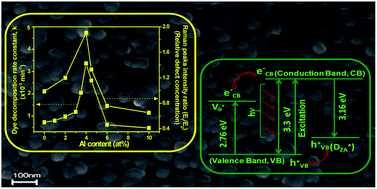
Al doped nanostructured zinc oxide thin films (thickness, 165 ± 5 nm) on silica glass were prepared from zinc acetate based solutions of varying dopant content (0 to 10 at% with respect to Zn). X-ray diffraction confirmed the presence of nanocrystalline hexagonal ZnO. On increasing the doping level, we observed a change in ZnO morphology (spherical, hexagon and plate-shaped) under field emission scanning and transmission electron microscopes and a gradual decrease of ZnO crystallite size (14.0 to ∼10 nm) vis-à-vis an enhancement of direct band gap energy of the films. Root mean square film surface roughness and chemical state of elements were studied by atomic force microscopy and X-ray photoelectron spectroscopy respectively. In addition to common intrinsic defects in ZnO, a defect (designated as D˙ZA, appearing as a paramagnetic singly negatively charged oxygen vacancy) was identified up to 4% doping from the appearance of photoluminescence emission at 398 nm and measurement of paramagnetic property of the films. Film photocatalytic activity towards Rhodamine 6G dye decomposition was performed under UV (254 nm) irradiation and the film with 4% doping (A4ZO) showed the highest value of first order decomposition rate constant. On increasing Al content, the trend of change of defect concentration (oxygen vacancies) analyzed by Raman spectra was found to be identical with the dye photodecomposition activity (PA) of the films. A major role of DZA˙ towards the PA was explored under visible light. We proposed the reaction mechanism of PA based on the experimental results. The A4ZO would be expected to decompose micro-organisms under visible light.


Introduction

With the growth of industries, environmental problems become a more and more serious concern globally. Nanostructured semiconductor oxide materials (NSOM)1–3 as efficient photocatalysts would be used in solving the problem economically for decomposition of organic pollutants (e.g. dyes, volatile organic compounds, detergents, pesticides etc.) on irradiation of light. One of the non-toxic, biocompatible and inexpensive NSOM is ZnO.4 In addition to the photocatalytic activity of NSOM, it has many applications2,5,6 such as in transparent conducting oxide (TCO) materials, UV and white light emitting phosphors, gas sensors for detection of humidity and several combustible gases, biosensors, bioimaging, drug delivery and piezoelectric transducers. Further, the high chemical and thermal stability4 of ZnO make the material suitable for application in high temperature as well as in corrosive environments.

The widespread applications of ZnO primarily based on its exceptional properties5,6 such as microstructural, electrical, optical, electronic, optoelectronic. Moreover, by doping with the elements belonging to group III (B, Al, etc) of periodic table, optical and photocatalytic properties can significantly be changed depending7–11 upon the nature and content of the element. This is because incorporation of doping element into the ZnO crystal, the lattice parameters and defects (intrinsic/extrinsic) concentration7–11 would change. The content of doping also depends upon the crystal size due to self purification12 in semiconductor nanocrystals. Depending upon the preparation method13 as well as doping,14 many defects13 have been identified in ZnO both theoretically and experimentally. Formation of the defects would occur within the band gap of ZnO (bulk direct band gap, 3.37 eV).15,16 These defects are generally characterized by photoluminescence studies.11,17 The nature and concentration of defects18 also influence the magnetic property of ZnO. Intentional creation of defects has also their own perspectives (usefulness).10,13,14,19 For example, it is generally accepted that oxygen vacancies function as electron acceptors19 which can trap the photogenerated electrons and therefore, the efficiency of the catalyst could be enhanced. In addition, the catalytic application can also be extended under visible light irradiation in presence of the defects.

Various defects including the oxygen vacancy can play an important role15,20–26 on the photocatalytic activity (PA) of ZnO. Further, PA also found to depend on concentration of oxygen vacancy. Sun et al.26 observed a higher photocatalytic activity due to the existence of high-level surface and subsurface oxygen vacancy in well-aligned single-crystalline ZnO nanobelt arrays on Si wafer. Also, Wang et al.22 reported an enhanced photocatalytic activity of ZnO nanoflowers due to the presence of large extent of oxygen vacancy which can able to separate the photogenerated electron–hole pairs.

Several ZnO film deposition techniques such as sputtering (e.g. rf sputtering, magnetron sputtering), CVD/PVD, sol–gel etc. are known. However, sol–gel is a facile and cost effective technique for tailoring film crystallinity, morphology and optical properties through several competing factors6,9 such as sol/solution chemistry, dopant content and nature, curing condition, etc. Many authors already also reported7,10,11,27 the morphology, optical, opto-electronic and electrical properties of aluminium zinc oxide (AZO) films. The film can also act a photocatalyst towards photodegradation of organic dyes but a very few reports11,28 are available in this concern. Very recently, Pradhan et al.11 reported the photocatalytic activity towards degradation of methyl orange on exposure of different light sources (UV, 380 nm; white light and sun light) of AZO thin film deposited by spray pyrolysis. They claimed a high rate of degradation (100% under UV and sunlight in 3 h irradiation) using 25% Al doped ZnO film as photocatalyst.

It is also known that the rate of decomposition29 of an organic dye depends upon its chemical structure30 and optimum amount of catalyst.31 Moreover, a photocatalyst would not give similar nature of decomposition for all the dyes even the measurement conditions remain same. In addition, most of the photocatalytic activities of powders15,19 have been reported on azo dyes.32–34 This is probably, 70% azo dyes use in textile industry35 and remaining 30% dyes including rhodamine 6G (Rh-6G)36 are mostly used as laser dyes. However, the thin film photocatalyst may find application in the area6 of human health and environment. To the best of our knowledge, the decomposition of Rh-6G dye using sol–gel based Al-doped ZnO thin films as photocatalyst seems not found in the literature.

Hence, in the present work, a systematic study was performed on Al doped nanostructured zinc oxide thin films derived from zinc acetate based precursor solutions of varying dopant content (0 to 10 at% with respect to Zn) to observe the effect of doping on crystallinity and lattice parameters, morphology and microstructure, optical (band gap and photoluminescence), magnetic and photocatalytic properties of the films. Photocatalytic activity of the films towards Rh-6G dye decomposition was studied under UV (254 nm) irradiation. In addition to common intrinsic defects of ZnO, a defect (designated as DZA˙, appeared as paramagnetic singly negatively charged oxygen vacancy) was identified up to 4% doping from the measurement of photoluminescence and paramagnetic property of the films. Moreover, on increasing doping level, the trend of change of defect concentration (oxygen vacancies) analyzed by Raman spectra was found identical with the dye photodecomposition activity of the films. Further, a major role of the D˙ZA defect towards photocatalytic activity was explored under visible light.

Experimental

Preparation of precursor solutions and thin films

All the precursor materials were used as received. The precursor solutions for zinc oxide film formation were prepared from zinc acetate dihydrate (Zn(CH3COO)2·2H2O, ZA, Fluka, 99.5%) and aluminium chloride hexahydrate (AlCl3·6H2O, AC, Fluka, 99.0%) as the sources of Zn and Al respectively. Iso-propanol (IP, for synthesis, Merck) and double distilled water (DDW; IP[thin space (1/6-em)]:[thin space (1/6-em)]DDW = 1.37 to 1.43, weight ratio) as solvents along with acetylacetone (acac, Merck, 98%; ZA[thin space (1/6-em)]:[thin space (1/6-em)]acac = 1[thin space (1/6-em)]:[thin space (1/6-em)]1, mol ratio) as solution stabilizer were used. The content of Al was varied from 0 to 10 at% with respect to Zn. However, the total oxide content kept fixed at 6 wt% in all the solutions. It was important to mention that the adherence of as-prepared solutions to the pure silica glass (Suprasil grade, Heraus, Germany, dimensions: 25 mm × 10 mm × 1 mm) used for thin films deposition was very poor. However, after ageing the solutions for ∼7 days a good adherence to the substrate was resulted. The solutions having Al contents 0, 1, 2, 3, 3.5, 4, 4.5, 6 and 10 were designated as SA0ZO, SA1ZO, SA2ZO, SA3ZO, SA3.5ZO, SA4ZO, SA4.5ZO, SA6ZO and SA10ZO respectively.

Thin films were deposited on pre-cleaned9 glass substrate by dipping technique (Dip Master-200, Chemat Technology Inc., USA) with a constant withdrawal speed of 12 cm min−1 utilizing the aged solutions. To get the oxide films, the as-coated samples were initially dried in an air oven at 60 °C followed by curing at 500 °C with 1 h soaking time under air atmosphere in an electrical furnace. The final films derived from the aged solutions, SA0ZO, SA1ZO, SA2ZO, SA3ZO, SA3.5ZO, SA4ZO, SA4.5ZO, SA6ZO and SA10ZO were designated as A0ZO, A1ZO, A2ZO, A3ZO, A3.5ZO, A4ZO, A4.5ZO, A6ZO and A10ZO respectively.

Characterization

Film physical thickness was measured using an auto gain Ellipsometer (Gaertner Auto-Gain Ellipsometer, model: L-116 B) equipped with a He–Ne red laser (wavelength, 632.8 nm). The thickness of the films found to increase slightly from 160 to 170 nm depending on Al content from 0 to 10%. X-ray diffraction (XRD) study of the films was done by Rigaku SmartLab using CuKα radiation (1.5406 Å) operating at 9 kW in the diffraction angle (2θ), 25 to 70°. The crystallite size of zinc oxide formed in the films was also calculated6 using Scherrer's equation. The film surface feature, clustered size of ZnO and tentative content of metals were analyzed by FESEM and FESEM-EDS (ZEISS, SUPRA™ 35VP). TEM measurements were carried out by Tecnai G2 30ST (FEI) electron microscope operating at 300 kV from the scratched off film onto 300 mesh carbon coated cupper grid. TEM/HRTEM and TEM-EDS were performed for analyses of particle size, crystal phase and content of metals. The films were also characterized by Atomic Force Microscope (AFM, Nanonics, Israel NSOM). From the AFM surface topography, the root mean square surface roughness (RMSSR) of the films was calculated by the available software of the equipment. UV-Vis-NIR spectrophotometer (Shimadzu UV-PC-3100; photometric accuracy: transmission ±0.3%, wavelength resolution, 0.10 nm) was used to measure UV-Vis absorption spectra of the films. Band gap energy (BGE) of the films was calculated6,9 from the respective absorption spectrum. Substrate corrected FTIR vibration spectra of the films were recorded using a FTIR instrument (Nicolet 5700, USA, wavenumber accuracy: ±4 cm−1). Perkin–Elmer (LS55) spectrofluorimeter was employed to measure the photoluminescence property of the films at room temperature. The magnetic property measurement was carried out at room temperature by employing a magnetometer (Vibrating Sample Magnetometer, Lake Shore, Model 7407) in the applied magnetic field range, −20 kOe to 20 kOe. Background magnetic contribution of the substrate was corrected from all the films. Individual magnetization (emu cm−3) data was calculated from the background corrected magnetic moment (emu), area of thin film and film thickness. Room temperature substrate corrected Raman spectral measurements (micro Raman, Renishaw inVia Raman microscope) was done using argon-ion laser with an incident wavelength of 514 nm as the excitation source. X-ray photoelectron spectra (XPS) of three representative samples, undoped (A0ZO), 4% doped (A4ZO) and 10% doped (A10ZO) films were carried out by employing PHI Versaprobe II Scanning XPS microprobe surface analysis system using Al-Kα X-rays (, 1486.6 eV; ΔE, 0.7 eV at room temperature). The energy scale of the spectrometer was calibrated with pure (Ag) samples and the pressure in the XPS analysis chamber was better than 5 × 10⁻¹⁰ mbar. The chemical state of each element present in the thin film was determined. The position of (C 1s) peak was taken as standard (with the binding energy of 284.5 eV).

Photocatalytic activity (PA) of the films towards degradation of Rhodamine 6G (Rh-6G) was studied in a custom built stainless steel UV (wavelength, 254 nm) curing chamber. The coated sample (total area, ∼3.5 cm2) was placed approximately 45° angle with the wall of borosilicate glass beaker of 100 ml capacity containing the solution of dye (10−5 M, Co) in double distilled water. The detailed PA measurement set up has already been reported elsewhere.6 We also carried out the PA of a specific film (A4ZO) under visible light irradiation. For this purpose, a tungsten bulb (200 W, Philips India) was used as a visible light source employing two cutoff glass filters (cutoff wavelengths, 393.5 nm and 412 nm), the details of the setup is given under the results and discussion (Fig. S4, ESI). In a certain time interval, ∼4 ml dye solution took out and visible absorption spectrum was recorded to find out the remnant concentration (C) of the dye with the help of a calibration curve of the dye solutions. The calibration curve was constructed by plotting dye concentration against absorbance (OD) at 527 nm peak wavelength of Rh-6G solutions obeying Lambert–Bayer's law. The PA of the films was analyzed by plotting ln(Co/C) (dye concentration; Co, initial and C, remnant) versus irradiation time. The rate constants of decomposition reaction (considering first order reaction kinetics) were calculated from the plots.

Results and discussion

X-ray diffraction (XRD) reflections (Fig. 1a) of the films revealed that all the films are crystalline in nature but the crystallinity of A2ZO and A3ZO films found relatively better than the other films as evidenced from the intensity of the reflections. However, the observed XRD reflections were fully matched with the hexagonal zinc oxide (h-ZnO) [JCPDS card 36-1451]. It was noteworthy to mention that no Al related crystal or compound8,11 was observed within the doping level. On increasing Al content, the peaks were found to be broadened and slightly red shifted with respect to the undoped film (A0ZO). The peak shifting may indicate the substitution of Zn(II) by Al(III) in h-ZnO crystal. The ionic size of Al(III) (0.51 Å) is smaller than Zn(II) (0.74 Å), hence a good amount of Al(III) could expect to substitute37 Zn(II) site in ZnO crystal. Further, lattice distortion (LD, decrease of lattice parameter, ‘a’ and ‘c’ values) due to incorporation of Al in ZnO could be happened and the LD should increase with increasing the amount of Al incorporation. In the present work, the value of ‘a’ and ‘c’ measured from the respective XRD peaks along <100> and <002> planes respectively was observed to decrease rapidly (inset, Fig. 1b) with increasing Al content up to approximately 4% (A4ZO) and in the next higher doping level, particularly for 6 and 10% of Al, a very little change in the lattice parameters was seen. Approximately similar value of lattice parameters as obtained in A6ZO and A10ZO films could be an evidence for preventing further incorporation of dopant into the nanostructured ZnO crystals. This result could be validated the above approximation of Al incorporation37–39 in ZnO crystal. It also appeared that although, we increase the doping level up to 10% but the Al entered into the Zn site up to a maximum of 4%. The crystallite size of h-ZnO was measured at 2θ value corresponding to <101> plane using Scherrer's equation6,9,39 and the size (Fig. 1b) was found to influence strongly upon Al doping level. The calculated crystallite size found to decrease (Fig. 1b) from 14.0 to 9.7 (±0.5) nm with increasing Al doping content from 0 to 10% respectively. A maximum of 4% Al considered to be entered into the ZnO crystal lattice and on further increase of doping the excess Al may reside at the grain boundary40 of ZnO in amorphous form. This excess dopant would prevent further crystal growth41 of ZnO. As a result, the crystallite size of ZnO decreased rapidly after 4% of Al doping. Also, the decrease of crystallite size might create an unfavourable condition12 that would lead to hinder further incorporation of Al in ZnO crystal.
image file: c3ra44612c-f1.tif
Fig. 1 (a) XRD reflections of undoped and doped ZnO films. (b) A plot shows the change of ZnO crystallite size with doping content (inset shows the change of hexagonal ZnO crystal lattice parameters, ‘a’ and ‘c’ with dopant content).

Different surface feature (Fig. 2) of the films was visualized from FESEM images. A change in shape and size of ZnO clusters (spherical, near hexagon and plate-like) was observed in different doping levels. On increasing Al content, the shape of ZnO clusters found from spherical (undoped, size range: 66–83 nm) to near hexagon (1% doped, size range of largest side: 499–832 nm) to plate-like (2–4% doped, average thickness: 60–80 nm) and finally to nearly spherical (≥6% doped, size range: 60–70 nm). The hexagon-like clusters were supposed to be floated on the bed of spherical particles while plate-like clusters were found to be embedded into the featureless matrix. The FESEM images of the films supported that the spherical clusters would be the primary one from which different shapes of ZnO clusters originated39 through unequal growth rate of polar and non-polar surfaces of hexagonal ZnO crystals by Ostwald ripening. This would happen39 due to different chloride (Cl) concentrations coming from aluminium chloride used in the precursor solutions.


image file: c3ra44612c-f2.tif
Fig. 2 FESEM images of undoped and doped ZnO films.

A change of ZnO film surface morphology was observed by FESEM (Fig. 2) study. To understand the variation of film surface roughness due to the change of surface morphology, AFM measurement was carried out. A plot of root mean square surface roughness (RMSSR) versus dopant content is shown in Fig. S6 (ESI) where the lowest and highest roughness value was found in 6% and 2% doped films respectively. In fact, in other films including 4% doped film (A4ZO), an approximately same roughness value was obtained. The plot also displays individual film 3D surface topography (insets, Fig. S6).

TEM image (Fig. 3a) of undoped film (A0ZO) shows agglomerated quasi-spherical ZnO nanoclusters. However, the agglomeration found to be diminished (Fig. 3b, c, f and g) in doped films. We calculated the average size of nanoclusters from the TEM images (histograms, insets of Fig. 3a and b for A0ZO and A1ZO respectively; Fig. 3d for A4ZO; HRTEM images in the inset of Fig. 3f and inset m of Fig. 3g for A6ZO and A10ZO respectively). The sizes were 21.7, 20.8, 16.8, 14.7 and 11 nm for A0ZO, A1ZO, A4ZO, A6ZO and A10ZO films respectively. The trend in change of the nanocluster size as a function of doping content also supported the XRD result (Fig. 1b). However, the size measured from TEM images was found always higher than the calculated size from the XRD reflections. This might be considered due to agglomeration42 towards clustered formation. A closed porous structure was found distinctly in the TEM image (Fig. 3b) of A1ZO film. Content (at%) of Zn and Al present in the films were analyzed by TEM-EDS analysis and found approximately same to the content used in the precursor solutions. As for example, the content of Zn (Zn-k) and Al (Al-k) in A4ZO film (Fig. 3e for A4ZO) was 95.0 ± 1.0 and 4.8 ± 0.8% respectively whereas in A10ZO film (inset n of Fig. 3g), these were 90.1 ± 1.0 and 9.90 ± 0.9% respectively.


image file: c3ra44612c-f3.tif
Fig. 3 TEM images (a), (b), (c), (f) and (g) of A0ZO, A1ZO, A4ZO, A6ZO and A10ZO films respectively. (a), (b) (insets) and (d) show nanostructured ZnO particle size distributions (histograms) of A0ZO, A1ZO and A4ZO films respectively. TEM-EDS of A4ZO and A10ZO films are displayed in (e) and the inset (n) of (g) respectively. Encircled parts of (f) (inset) and inset (m) of (g) indicate the respective HRTEM images of A6ZO and A10ZO films.

Fig. 4 shows the substrate corrected FTIR spectra of the films. In all the films, a strong vibration appeared at 414 cm−1 indicated the presence of h-ZnO43 which supported the XRD result (Fig. 1a). Moreover, the spectral region, 550–450 cm−1 of Zn–O stretching vibration9 found to broaden with respect to the undoped film. This would be due to incorporation of Al into the ZnO crystal lattice. Although, no clear FTIR vibration for Al–O was found up to 6% doped films but a weak and broad vibration appeared at ∼805 cm−1 in A10ZO. This might be an indication for the presence of Al–O44 in the film network.


image file: c3ra44612c-f4.tif
Fig. 4 Substrate corrected FTIR spectra of undoped and doped ZnO films.

It is known that absorption co-efficient (α) and optical band gap energy (, Eg) are interrelated9 for a direct transition semiconductor, for example, ZnO. The Eg of the films was calculated from eqn (1). Individual α value was determined using respective UV-visible absorption and film physical thickness. Finally, the plot of (αhν)2 versus hν was drawn (Fig. 5a) and observed that the plots are parabolic in nature with two distinct inflexions indicated two transitions occurring in ZnO film. At the inflexion, the tangential extrapolation of the linear part of the plot to X-axis, (αhν)2 = 0 gives the Eg value. Among the inflexions, one is located at ∼3.3 eV for all the films. This would correspond9 to the bulk Eg of ZnO. Another Eg (inset, Fig. 5a) was observed at 3.47, 3.57, 3.62, 3.67, 3.70, 3.81 and 3.88 eV for 0, 1, 2, 3, 4, 6 and 10% doped films respectively. This could be related due to the effect of size9 of nanostructured ZnO.

 
αhν = A(Eg)1/2 (1)
where A is a constant.


image file: c3ra44612c-f5.tif
Fig. 5 (a) A plot of (αhν)2 versus hν for direct band gap determinations of A4ZO film on silica glass (inset, a plot of band gap energy with dopant content). (b) Photoluminescence (PL) spectra (λex. = 340 nm) of undoped and doped ZnO films on pure silica glass (inset shows PL excitation spectrum fixing the PL emission at 424 nm of A4ZO film).

All the films showed UV-Vis photoluminescence (PL) emissions (Fig. 5b) when excited at 340 nm (Inset, Fig. 5b). Undoped ZnO film (A0ZO) showed an intense emission at ∼424 nm in addition to the emissions at ∼398 nm (broad shoulder), ∼450 nm, ∼485 nm and ∼530 nm. The intensity of emission at 398 nm (Table S1, ESI) with respect to the other emissions found to gradually increase with doping and reached a maximum value in 4% doped film. Although, the emission at 398 nm found to be nearly disappeared in ≥6% doped films but a new UV PL emission at 376 nm (∼3.30 eV) was appeared. However, except the emission at 376 nm, the intensity of the emissions appeared above 400 nm found to decrease in ≥6% doped films. In addition, a shifting of the emission at ∼450 nm to ∼456 nm was noticed in ≥6% doped films. The UV PL emission at 376 nm corresponded to band to band transition11 through the recombination of electrons with holes in the valence band as free exciton recombination whereas the emission at 398 nm would consider as crystal defect (designated as DZA˙, appeared as singly negatively charged oxygen vacancy like image file: c3ra44612c-t1.tif, discussed later). Interestingly, in ≥6% doped films; the intensity of emission at 376 nm was always higher than all the visible emissions. It is known that the emission at 376 nm, a characteristic UV emission45 that could generally be appeared in low concentration of crystal defects in ZnO. Therefore, it would suggest11 that there would be a very low concentration of defects including the DZA˙ in ≥6% doped (A6ZO and A10ZO) films. Previously, some researchers also reported the UV PL emission including the peak at 398 nm as band edge emission45–47 of nanostructured ZnO. Very recently, an important remark on the 398 nm emission in Sn doped ZnO film has been given by Shi et al.48 They observed that the intensity of the emission increased with doping level and described the defect as Sn related doubly ionized donor formed in the deep states of ZnO band gap. Also, in Y doped ZnO nanoparticles, the same emission was reported.45 In fact, Yu et al.49 noticed the PL emission at 398 nm along with 378 and 420 nm in indium oxide nanofibers and demonstrated the emissions originating from different energy levels of oxygen vacancies. However, in the present work, we observed the emission in undoped ZnO film and the intensity of the emission increased with doping level of up to 4%. Therefore, Al doping could tailor the concentration of the defect within the band gap of ZnO (scheme, Fig. 10b). However, the defect already originated during the film deposition process. The defect would function as a singly ionized donor similar to the defect in Sn doped ZnO (doubly ionized donor)48 and would behave as hole scavengers in the Al doped ZnO. However, it could not be understood for the disappearance of the emission in ≥6% doped films.

Generally, five intrinsic defects (oxygen and zinc interstitials, oxygen and zinc vacancies and antisite oxygen)13 could be formed within the band gap of ZnO. These defects could able to generate PL emissions after excitation with photons. However, the formation of the defects was dependent on preparative methods13,45 and doping.14 In this work (Fig. 5b), single ionized (singly positively charged) oxygen vacancy (image file: c3ra44612c-t2.tif) was characterized from the appearance of PL emission at ∼450 nm (ref. 50) and its red shifting might be related to the change in defect concentration.45 Moreover, the presence of zinc interstitials (Zni)13 was also supported from the PL emission at 424 nm. Further, the existence of neutral oxygen vacancy (image file: c3ra44612c-t3.tif) would be ascertained from the observation of emission at 530 nm.51,52 Also, the emission at 485 nm supported50,53 the formation of antisite oxygen. Perhaps, singly positively charged oxygen vacancy (image file: c3ra44612c-t4.tif) and/or neutral oxygen vacancy (image file: c3ra44612c-t5.tif) would be the source54,55 of the DZA˙ defect. Anyhow, the enhancement of DZA˙ defect concentration (Table S1, ESI) would proceed via a process of accepting electron/(s) by image file: c3ra44612c-t6.tif and/or image file: c3ra44612c-t7.tif charge state/s from the conduction band of nanostructured ZnO crystals. Consequently, the process would be accelerated on increasing the number of conduction electrons which believed to be a maximum at the Al doping level of 4%.

Presence of various defects (DZA˙, zinc interstitials, antisite oxygen, neutral oxygen vacancy, singly positively charged oxygen vacancy) was identified by the PL spectra (Fig. 5b) of the films. It was also found that the relative concentration of DZA˙ (calculated from the PL emission peak intensity) (Table S1, ESI) found to increase on doping level (up to 4%). ZnO is known18 to be a diluted magnetic semiconductor (DMS). One can tailor the nature and concentration of defects18 as well as the magnetic property through suitable doping. Hence, measurement of magnetic property (Fig. 6) was done on three representative samples (A0ZO, A4ZO and A10ZO) to realize the effect of the defects, especially the defects of paramagnetic in nature on the magnetic property of the films. Generally, five charged states of oxygen vacancies,55 termed as image file: c3ra44612c-t8.tif, image file: c3ra44612c-t9.tif, image file: c3ra44612c-t10.tif, image file: c3ra44612c-t11.tif and image file: c3ra44612c-t12.tif would possible to form in oxides. These charge states correspond to zero, one, two, three and four electrons in the vicinity of the oxygen vacancies respectively. Therefore, the only image file: c3ra44612c-t13.tif, and image file: c3ra44612c-t14.tif oxygen vacancies would be considered as paramagnetic states due to the presence of unpaired electrons. It was also reported that zinc interstial as identified from PL spectra (Fig. 5b) in the present work was diamagnetic56 owing to the electron configuration ending with 4s2. The presence of antisite oxygen (as characterized by PL) in 2-charged state like lattice oxygen (O2−) and/or interstitials oxygen (O2−) in h-ZnO would be diamagnetic.56 However, some oxygen vacancies54–57 (singly positively charged, image file: c3ra44612c-t15.tif and singly negatively charged, image file: c3ra44612c-t16.tif) would be paramagnetic. It should be noted that the image file: c3ra44612c-t17.tif state was recognized from the observation of PL emission at 450 nm (Fig. 5b) while the DZA˙ defect was identified from the emission at 398 nm. We considered, the DZA˙ defect as singly negatively charged oxygen vacancy, like image file: c3ra44612c-t18.tif. A justification on the proposition could be given on the basis of magnetic property measurement. At 15 kOe applied magnetic field, the A4ZO film, showed highest paramagnetic contribution in terms of magnetization value, 16.79 ± 1.13 emu cm−3 (Fig. 6b) whereas in the A0ZO and A10ZO films, the values were 2.62 ± 0.11 (Fig. 6a) emu cm−3 and 2.33 ± 0.24 emu cm−3 (with weak ferromagnetic ordering) (Fig. 6c) respectively. Thus, the magnetization value obtained in A4ZO is more than 6 times higher than the other films. This could strongly support the enhancement of paramagnetic defect concentration in 4% doped film (A4ZO). As the PL study (Fig. 5b and Table S1, ESI) already evidenced the increase in concentration of DZA˙ with respect to image file: c3ra44612c-t19.tif, hence, the highest paramagnetic property could be due to the highest concentration of DZA˙ defect in A4ZO. On the other hand, a weak ferromagnetic ordering (Fig. 6c) in absence of DZA˙ observed in A10ZO would be due to the presence of other defects.58 Probably, the paramagnetic DZA˙ defect would be responsible for preventing the ferromagnetic ordering in A0ZO and A4ZO ZnO films.


image file: c3ra44612c-f6.tif
Fig. 6 Substrate corrected magnetization versus applied magnetic field curves of undoped and doped ZnO films.

XPS study of three representative samples, undoped (A0ZO), 4% doped (A4ZO) and 10% doped (A10ZO) films were performed (Fig. 7 and S1, ESI). The position of binding energy signals (Fig. 7a) for Zn2p1/2and Zn2p3/2 core levels in A0ZO, A4ZO and A10ZO films were observed at 1044.65 ± 0.05 eV and 1021.9 ± 0.1 eV respectively. The difference between the two peaks is 23.1 ± 0.1 eV, matched well with the reported48 value for Zn(II). A broad signal of O 1s (Fig. 7b and c and S1b, ESI) was observed in both the films but the signal for A0ZO film was more asymmetric in nature than A4ZO and A10ZO films. Moreover, the broad signals could be resolved into three prominent Gaussian peaks centred at 530.2 ± 0.1 eV (S1), 531 ± 0.05 eV (S2) and 532.2 ± 0.1 eV (S3) for A0ZO film (Fig. 7b); 530.5 ± 0.2 eV (S1), 531.2 ± 0.1 eV (S2) and 532.2 ± 0.1 eV (S3) for A4ZO film (Fig. 7c) and 530.2 ± 0.1 eV (S1), 531.2 ± 0.1 eV (S2) and 532.2 ± 0.1 eV (S3) for A10ZO film (Fig. S1b, ESI). The appearance of S1 was due to O2− ions59 of wurtzite hexagonal ZnO as evident from XRD (Fig. 1a) while S2 could relate to O2− ions of oxygen deficient ZnO. Further, the S3 peak ascribed to the existence of loosely bound oxygen from carbonate, adsorbed water or oxygen molecules on the film surface. The S1, S2 and S3 peaks matched well with the reported values.59 On the other hand, the maximum concentration of O2− signal (S2) at ∼531 eV (due to oxygen deficiency) with respect to total oxygen signal was observed (Table S2, ESI) in A4ZO film. This result also supported the PL data where the relative emission peak intensity at 398 nm (DZA˙ defect, appeared as singly negatively charged oxygen vacancy) increased (Table S1, ESI) up to the doping level of 4%. The binding energy signals (Fig. 7d) for Zn3p and Al2p core levels observed prominently in A4ZO film. However, the signal for Al2p core level became very strong (Fig. S1a, ESI) in A10ZO film. This could be due to the increase of Al doping level (2.5 times higher than A4ZO). The binding energy peak (symmetric in nature) for Al2p3/2 core level was found at 74.1 ± 0.05 eV in the doped films. The observed peak was slightly lower than the reported value of stoichiometric Al2O3, suggested the presence of oxygen deficiency in the film network.


image file: c3ra44612c-f7.tif
Fig. 7 XPS data of undoped and doped ZnO films. (a) Typical XPS data for the binding energies of Zn2p3/2 and Zn2p1/2 core levels; (b) and (c) show the binding energies of O 1s and its Gaussian-fitted components for A0ZO and A4ZO respectively; (d) shows the binding energies of Zn3p along with Al2p core levels in A4ZO film (inset shows the encircled magnified portion of the Al2p signal).

ZnO is an n-type semiconductor oxide14 due to the presence of natural oxygen vacancies along with other common (intrinsic) defects. These could be tailored by incorporation of dopant (e.g. Y into ZnO crystal). In the periodic table of elements, ‘Al’ belongs to the same group (Group IIIA) of ‘Y’. In the present work, the XRD analysis (inset of Fig. 1b) already confirmed a maximum amount, ∼4% of Al entered into Zn site of hexagonal ZnO. Hence, the introduction of Al in ZnO crystal, there could be a change in concentration of defects depending upon the content of incorporated dopant. On the other hand, by Raman spectral study, the defect concentration (oxygen vacancies)60 in addition to the active mode of vibrations in h-ZnO could be better understood. Therefore, we performed the Raman study on the Al doped ZnO films. The equation for optical phonon vibrations of hexagonal wurtzite ZnO crystal at the Γ-point can be expressed by the irreducible representation9 as shown in eqn (2),

 
Γ = A1 +2B1 + E1 + 2E2, (2)
where A1 and E1 modes are both IR and Raman active which split into longitudinal optical (LO) and transverse optical (TO) components. However, E2 mode is only Raman active while B1 is forbidden. The Raman spectra of the films, A0ZO, A4ZO, A6ZO and A10ZO are shown in Fig. 8 whereas the spectra of A1ZO and A2ZO films are displayed in Fig. S2, ESI. In undoped film (A0ZO), two prominent peaks observed at 437 cm−1 and 582 cm−1 but in doped films, additional two new peaks were noticed at 329 cm−1 (ascribed to TO−TA (M)) and at 657 cm−1 (weak, attributed to E2 (low) + B1 (high)).16 Anyhow, the A10ZO film showed a new peak at 556 cm−1 (very sharp) which would be related to the density of states (DOS)61 in ZnO. The Raman vibration at 437 cm−1 indicated the characteristics9 of wurtzite ZnO crystal in E2(high) mode. The E1(LO) appeared at 582–584 cm−1 related to the defects (oxygen vacancies) present in the nanostructured ZnO film. The slightly red shifting of E1(LO) to 584 cm−1 in A10ZO film would consider due to the change in size9 of nanostructured h-ZnO as evidenced from XRD (Fig. 1b) and TEM analyses (Fig. 3). On the other hand, the change of intensity ratio (R), E1(LO)/E2(high) could be an useful tool to explain60 the variation of defect concentration in hexagonal ZnO. It could believe that higher the R value higher will be the defect concentration. We determined the R value from the substrate corrected Raman spectra and the R values were plotted against the doping content (inset, Fig. 8). The calculated values of R are 1.0, 1.92, 0.76 and 0.65 (±0.05) for the A0ZO, A4ZO, A6ZO and A10ZO films respectively. From the R values, it revealed that the highest defect concentration (oxygen vacancies) was present in A4ZO film. Accordingly, a good photocatalytic activity of A4ZO film towards organic dye decomposition could be expected (discussed later) even under visible light irradiation.


image file: c3ra44612c-f8.tif
Fig. 8 Substrate corrected Raman spectra of undoped and doped ZnO films. Inset shows a plot of Raman peaks intensity ratio of E1/E2 with dopant content.

Photodecomposition study of Rh-6G dye (10−5 M) (Fig. 9, 10a and S3 to S5 of ESI) using the films as photocatalyst was performed under UV (λ, 254 nm) and visible light irradiations. The photocatalytic activity for 4% doped film (A4ZO) was studied on exposure of visible light employing cut off glass filters (Filter-1: cut off wavelength, 393.5 nm and Filter-2: cut off wavelength, 412 nm). Considering the first order reaction kinetics, the dye decomposition (Fig. 9a, S3, S5a (inset) and S5, ESI) rate constant (k) was measured (Fig. 9b, c and d and S5a, ESI). A plot (Fig. 10a) of k value (in the order of 10−4 min−1) against doping content was drawn. From the plot, it is noticed that the ‘k’ value rapidly increased on increasing dopant content up to 4% (in A4ZO film) and then decreased on further increase of the dopant content. However, the lowest ‘k’ value was found in 10% doped (A10ZO) film would arise due to the faster rate of recombination23,62 of photogenerated electrons and holes in relatively lowest defect concentration (mainly DZA˙) of nanostructured ZnO. On the other hand, the generation of highest rate of photodecomposition (highest k value) in A4ZO would consider as the presence of highest defect concentration as confirmed from Raman spectral analysis (inset of Fig. 8a and 10a) which prevented the faster rate of recombination23,62 of photogenerated electrons and holes. As a result the enhancement of the photocatalytic activity could be occurred.


image file: c3ra44612c-f9.tif
Fig. 9 (a) Remnant dye (Rh-6G) concentration versus UV (λ254 nm) exposure time using undoped and doped films as photocatalysts. (b), (c) and (d) show the determination of first order rate constant ‘k’ of the photodecomposition of Rh-6G using the photocatalysts, A0ZO, A4ZO and A10ZO films respectively.

image file: c3ra44612c-f10.tif
Fig. 10 (a) Plots show the change of defect concentration of the films calculated from Raman spectral analysis and first order decomposition rate constant of Rhodamine 6G dye under UV (λ, 254 nm) with dopant content. (b) Proposed reaction mechanism on the photocatalytic activity of the films.

Generally, photocatalytic activity of semiconductor oxide depends upon many factors6,11,23,63 such as surface area (inversely related to size and directly proportional to the band gap energy), surface structure (related to film surface morphology), defect concentration, etc. In the present work, the A4ZO film showed the highest photocatalytic activity although the lowest size of ZnO was found in A10ZO film. It was also found that the size of ZnO gradually decreased with increasing Al content as evidenced from XRD (Fig. 1) and TEM (Fig. 3) vis-à-vis the direct band gap energy gradually increased (Fig. 5). Hence, the change of size/band gap energy of ZnO would not be a deciding factor to control the photodecomposition activity of the dye. In addition, the change of root means square surface roughness (relate to surface structure) measured from AFM for a fixed area of the films (Fig. S6, ESI) would not support the change of the dye decomposition rate constant. This is because the lowest and highest surface roughness value were found in 6% (A6ZO) and 2% doped (A2ZO) films respectively whereas approximately same value was obtained in the other films including 4% doped (A4ZO) film. Further, it is known that the faster rate of electron–hole recombination63 could be prevented by introduction of surface defect in ZnO crystal. As a result, the enhancement of photocatalytic activity could be expected. This intentional defect creation in semiconductor photocatalysts could also be an attractive way of photocatalytic studies63 under visible light irradiation. In this work, the Raman spectral analysis showed a systematic change of defect concentration (oxygen deficiencies) with doping content (inset, Fig. 8 and 10a) and a maximum defect concentration was found in A4ZO film. On increasing dopant content, the trend (Fig. 10a) of change in defect concentration was identical to the trend of change of the dye decomposition rate constant. This result strongly suggested that the defect concentration controlled the rate of the dye decomposition. However, it was absolutely necessary to understand the specific role of the DZA˙ defect as one of the oxygen deficiencies in comparison to defects such as singly positively charged oxygen vacancy, neutral oxygen vacancy, interstitial Zn, antisite oxygen in ZnO as already evidenced from PL (Fig. 5b) and XPS (Fig. 7b and c and S1b, ESI) spectral study particularly in A4ZO film. To find out the specific role of the DZA˙ defect towards the dye decomposition, we used cut off glass filters, Filter-1 (cut off wavelength, 393.5 nm) and Filter-2 (cut off wavelength, 412 nm) (Fig. S4b) with the identical visible transmittance during the measurement of photocatalytic activity of the film under visible light irradiation (scheme: Fig. S4a). Using Filter-1, we obtained the ‘k’ value (3.0 × 10⁻³ min−1) (inset, Fig. S5a) slightly lower than the ‘k’ value (3.3 × 10⁻³ min−1 measured under UV irradiation, Fig. 9c) using A4ZO film as photocatalyst. However, a very low rate of dye decomposition (Fig. S5b) was found when the Filter-2 was used. This result could confirm the major role of the DZA˙ defect towards the dye decomposition. The lowest rate of the dye decomposition using Filter-2, would be due to inactiveness of the DZA˙ defect under lower energy (below ∼3.0 eV, 412 nm) of irradiation than the minimum energy (∼3.12 eV, 398 nm) required for activation of the defect (DZA˙) towards photocatalytic decomposition of the dye. It is known that the oxygen vacancies as electron acceptors19 could trap the photogenerated electrons. In the present work, the DZA˙ defect would function as hole scavengers because from the magnetic moment study (Fig. 6), it appeared as paramagnetic image file: c3ra44612c-t20.tif like charge state (singly negatively charged oxygen vacancy). In addition, from the PL spectral study, it was verified that the other common defects including singly positively charged oxygen vacancy, image file: c3ra44612c-t21.tif were present in all the films. These would also take part in the photocatalytic activity. However, our experimental results on the dye decomposition under visible light using cut off glass filters clearly demonstrated that these defects including image file: c3ra44612c-t22.tif found to be less effective than the DZA˙ defect. Hence, a major contribution of the DZA˙ defect together with a minor role of the other defects including singly positively charged oxygen vacancy of sol–gel based nanostructured Al doped ZnO films was found in the photocatalytic decomposition of Rh-6G dye.

On the basis of our experimental results, a scheme19 for the mechanism of photocatalytic reactions using the nanostructured ZnO film as photocatalyst is given in Fig. 10b.

Conclusion

Thin films of dip-coated Al doped nanostructured zinc oxide on silica glass were prepared with varying dopant content (0–10 at% with respect to Zn). All the films were nanocrystalline and enriched with hexagonal ZnO. On increasing the doping level, the size of nano ZnO particles was found to decrease vis-à-vis a gradual enhancement of direct band gap energy and a change in ZnO particle morphology (spherical, hexagonal and plate-like) as well as film surface roughness were observed. In addition to common intrinsic defects in ZnO, a defect (designated as DZA˙, appearing as paramagnetic singly negatively charged oxygen vacancy) was identified from the photoluminescence emission spectra and the paramagnetic property of the films. Film photocatalytic activity (PA) towards Rh-6G dye decomposition was performed under UV (λ, 254 nm) irradiation and the film doped with 4% Al (A4ZO) showed the highest decomposition activity. On increasing doping level, the trend of change of defect concentration (oxygen vacancies) was found to be identical with the dye photodecomposition activity (PA) of the films. Among the common defects found in ZnO, a major role of the DZA˙ was found towards the PA. The A4ZO would be expected to decompose micro-organisms under visible light.

Acknowledgements

The authors are grateful to Director, CSIR-CGCRI, Kolkata for his kind support and encouragement. The authors, MP and SB thankfully acknowledge UGC and CSIR, Govt. of India for providing their Ph.D. research fellowships under NET Fellowship scheme. The authors also acknowledge the help rendered by Nanostructured Materials Division and Electron Microscopy Section for Raman, magnetic property measurements and microstructural characterizations respectively. The work had been done under Institute funded In-house project (no. OLP0299).

References

  1. M. R. Hoffmann, S. T. Martin, W. Choi and D. W. Bahnemann, Chem. Rev., 1995, 95, 69 CrossRef CAS.
  2. C. Wang, X. Wang, B.-Q. Xu, J. Zhao, B. Mai, P. Peng, G. Sheng and J. Fu, J. Photochem. Photobiol., A, 2004, 168, 47 CrossRef CAS PubMed.
  3. T. S. Natarajan, K. Natarajan, H. C. Bajaj and R. J. Tayade, J. Nanopart. Res., 2013, 15, 1669 CrossRef.
  4. G. G. Rusu, A. P. Rambu, V. E. Buta, M. Dobromir, D. Luca and M. Rusu, Mater. Chem. Phys., 2010, 123, 314 CrossRef CAS PubMed.
  5. S. Dutta and B. N. Ganguly, J. Nanobiotechnol., 2012, 10, 29 CrossRef CAS PubMed.
  6. M. Pal, S. Bera and S. Jana, J. Sol–Gel Sci. Technol., 2013, 67, 8 CrossRef CAS PubMed.
  7. S. Tewari and A. Bhattacharjee, PRAMANA – J. Phys., 2011, 76, 153 CrossRef CAS.
  8. A. Shui, S. Wang, H. Wang and X. Cheng, J. Ceram. Soc. Jpn., 2009, 117, 703 CrossRef CAS.
  9. S. Jana, A. S. Vuk, A. Mallick, B. Orel and P. K. Biswas, Mater. Res. Bull., 2011, 46, 2392 CrossRef CAS PubMed.
  10. E. M. Likovich, R. Jaramillo, K. J. Russell, S. Ramanathan and V. Narayanamurt, Appl. Phys. Lett., 2011, 99, 151910 CrossRef PubMed.
  11. P. Pradhan, J. C. Alonso and M. Bizarro, Int. J. Photoenergy, 2012, 2012, 780462 CrossRef PubMed.
  12. G. M. Dalpian and J. R. Chelikowsky, Phys. Rev. Lett., 2006, 96, 226802 CrossRef.
  13. L. Zhao, J.-S. Lian, Y.-h. Liu and Q. Jing, Trans. Nonferrous Met. Soc. China, 2008, 18, 145 CrossRef CAS.
  14. C.-Y. Kung, S.-L. Young, H.-Z. Chen, M.-C. Kao, L. Horng, Y.-T. Shih, C.-C. Lin, T.-T. Lin and C.-J. Ou, Nanoscale Res. Lett., 2012, 7, 372 CrossRef PubMed.
  15. Y. Zheng, C. Chen, Y. Zhan, X. Lin, Q. Zheng, K. Wei, J. Zhu and Y. Zhu, Inorg. Chem., 2007, 46, 6675 CrossRef CAS PubMed.
  16. K. J. Chen, T. H. Fang, F. Y. Hung, L. W. Ji, S. J. Chang, S. J. Young and Y. J. Hsiao, Appl. Surf. Sci., 2008, 254, 5791 CrossRef CAS PubMed.
  17. S. Ananthakumar, S. Anas, J. Ambily and R. V. Mangalaraja, J. Ceram. Process. Res., 2010, 11, 164 Search PubMed.
  18. W. Cheng and X. Ma, J. Phys.: Conf. Ser., 2009, 152, 012039 CrossRef.
  19. J. Wang, P. Liu, X. Fu, Z. Li, W. Han and X. Wang, Langmuir, 2009, 25, 1218 CrossRef CAS PubMed.
  20. G. Marci, V. Augugliaro, M. J. Lopez-Munoz, C. Martin, L. Palmisano, V. Rives, M. Schiavello, R. J. D. Tilley and A. M. Venezia, J. Phys. Chem. B, 2001, 105, 1033 CrossRef CAS.
  21. J.-Z. Kong, A.-D. Li, H.-F. Zhai, Y.-P. Gong, H. Li and D. Wu, J. Solid State Chem., 2009, 182, 2061 CrossRef CAS PubMed.
  22. Y. Wang, X. Li, N. Wang, X. Quan and Y. Chen, Sep. Purif. Technol., 2008, 62, 727 CrossRef CAS PubMed.
  23. R. Ullah and J. Dutta, J. Hazard. Mater., 2008, 156, 194 CrossRef CAS PubMed.
  24. Y. Zheng, L. Zheng, Y. Zhan, X. Lin, Q. Zheng and K. Wei, Inorg. Chem., 2007, 46, 6980 CrossRef CAS PubMed.
  25. K. Maeda, T. Takata, M. Hara, N. Saito, Y. Inoue, H. Kobayashi and K. Domen, J. Am. Chem. Soc., 2005, 127, 8286 CrossRef CAS PubMed.
  26. T. Sun, J. Qiu and C. Liang, J. Phys. Chem. C, 2008, 112, 715 CAS.
  27. K.-C. Hsiao, S.-C. Liao and Y.-J. Chen, Mater. Sci. Eng., A, 2007, 447, 71 CrossRef PubMed.
  28. M. Bizarro, Appl. Catal. B, 2010, 97, 198 CrossRef CAS PubMed.
  29. K. Zhang and W.-C. Oh, J. Korean Ceram. Soc., 2009, 46, 561 CrossRef CAS.
  30. S. A. Abo-Farha, J. Am. Sci., 2010, 6, 130 Search PubMed.
  31. I. Bhati, R. Ameta, P. B. Punjabi and S. C. Ameta, Int. J. Chem. Sci., 2010, 8, 2784 CAS.
  32. C. Zhu, L. Wang, L. Kong, X. Yang, L. Wang, L. Zheng, F. Chen, F. Maizhi and H. Zong, Chemosphere, 2000, 41, 303 CrossRef CAS.
  33. I. K. Konstantinou and T. A. Albanis, Appl. Catal., B, 2004, 49, 1 CrossRef CAS PubMed.
  34. Y. Liu, X. Chen, J. Li and C. Burda, Chemosphere, 2005, 61, 11 CrossRef CAS PubMed.
  35. S. Sethi, Shubhum, M. M. Malviya, N. Sharma and S. Gupta, Univers. J. Environ. Res. Technol., 2012, 2, 582 CAS.
  36. S. Salleres, F. L. Arbeloa, V. Matinez, T. Arbeloa and I. L. Arbeloa, J. Phys. Chem. C, 2009, 113, 965 CAS.
  37. A. Sedky, A. Al-Sawalha and A. M. Yassin, Egypt J. Solid., 2008, 31, 205 Search PubMed.
  38. S. Jana and P. K. Biswas, Mater. Chem. Phys., 2009, 117, 511 CrossRef CAS PubMed.
  39. S. Bera, M. Pal, S. Sarkar and S. Jana, Appl. Surf. Sci., 2013, 273, 39 CrossRef CAS PubMed.
  40. S. Mondal, K. P. Kanta and P. Mitra, J. Phys. Sci., 2008, 12, 221 Search PubMed.
  41. M. Tanahashi, M. Ito, M. Murao and A. Iga, Jpn. J. Appl. Phys., 1997, 36, L573 CAS.
  42. I. C. Baek, S. I. Seok, N. C. Pramanik, S. Jana, M. A. Lim, B. Y. Ahn, C. J. Lee and J. Y. Jeong, J. Colloid Interface Sci., 2007, 310, 163 CrossRef CAS PubMed.
  43. S. R. Ready, S. A. Reddy, B. Radhakrishna and S. Uthanna, Cryst. Res. Technol., 2012, 47, 1095 CrossRef.
  44. V. Sontevska, G. Jovanovski, P. Makreski, A. Raskovska and B. Soptrajanvo, Acta Chim. Slov., 2008, 55, 757 CAS.
  45. M. Gao, J. Yang, L. Yang, Y. Zhang, J. Lang, H. Liu, H. Fan, Y. Sun, Z. Zhang and H. Song, Superlattices Microstruct., 2012, 52, 84 CrossRef CAS PubMed.
  46. Q. P. Wang, D. H. Zhang, Z. Y. Xue and X. T. Hao, Appl. Surf. Sci., 2002, 201, 123 CrossRef CAS.
  47. K.-F. Lin, H. M. Cheng, H.-C. Hsu, L.-J. Lin and W.-F. Hsieh, Chem. Phys. Lett., 2005, 409, 208 CrossRef CAS PubMed.
  48. X. Shi, X. Zhao, L. Duan, H. Sun, J. Liu, X. Bai, M. Guan, M. Cao and J. Liu, J. Sol–Gel Sci. Technol., 2013, 66, 301 CrossRef CAS PubMed.
  49. D. Yu, S.-H. Yu, S. Zhang, J. Zuo, D. Wang and Y. Qian, Adv. Funct. Mater., 2003, 13, 497 CrossRef CAS.
  50. T. Gao, G. Meng, Y. Tian, S. Sun, X. Liu and L. Zhang, J. Phys.: Condens. Matter, 2002, 14, 12651 CrossRef CAS.
  51. J. D. Ye, S. L. Gu, S. M. Zhu, F. Qin, S. M. Liu, W. Liu, X. Zhou, L. Q. Hu, R. Zhang, Y. Shi and Y. D. Zheng, J. Appl. Phys., 2004, 96, 5308 CrossRef CAS PubMed.
  52. M. Willander, O. Nur, J. R. Sadaf, M. I. Qadir, S. Zaman, A. Zainelabdin, N. Bano and I. Hussain, Materials, 2010, 3, 2643 CrossRef CAS.
  53. X. Wei, R. Zhao, M. Shao and J. Huang, Nanoscale Res. Lett., 2013, 8, 112 CrossRef PubMed.
  54. K. M. Wong, S. M. Alay-e-Abbas, Y. Fang, A. Shaukat and Y. Lei, J. Appl. Phys., 2013, 114, 034901 CrossRef PubMed.
  55. D. M. Ramo, J. L. Gavartin, A. L. Shluger and G. Bersuker, Phys. Rev. B: Condens. Matter Mater. Phys., 2007, 75, 205336 CrossRef.
  56. H. Kaftelen, K. Ocakoglu, R. Thomann, S. Tu, S. Weber and E. Erdem, Phys. Rev. B: Condens. Matter Mater. Phys., 2012, 86, 014113 CrossRef.
  57. Springer Handbook of Materials Measurement Methods, ed. H. Czichos, T. Saito and L. Smith,  DOI:10.1007/978-3-540-303008_1, Springer-Verlag, 2006.
  58. S. Karamat, R. S. Rawat, P. Lee and T. L. Tan, J. Phys.: Conf. Ser., 2010, 200, 072045 CrossRef.
  59. M. Chen, X. Wang, Y. H. Yu, Z. L. Pei, X. D. Bai, C. Sun, R. F. Huang and L. S. Wen, Appl. Surf. Sci., 2000, 158, 134 CrossRef CAS.
  60. D. Wang and N. Reynolds, ISRN Condens. Matter Phys., 2012, 2012, 950354 Search PubMed.
  61. W. Gebicki, K. Osuch, C. Jastrzebski, Z. Golacki and M. Godlewski, Superlattices Microstruct., 2005, 38, 428 CrossRef CAS PubMed.
  62. J. Liquiang, Q. Yichun, W. Baiqui, L. Shudan, F. Baojiang and S. Jiashong, Sol. Energy Mater. Sol. Cells, 2006, 90, 1773 CrossRef PubMed.
  63. S. Baruah, R. F. Rafique and J. Dutta, NANO: Brief Reports and Reviews, 2008, 3, 399 CAS.

Footnote

Electronic supplementary information (ESI) available. See DOI: 10.1039/c3ra44612c

This journal is © The Royal Society of Chemistry 2014
Click here to see how this site uses Cookies. View our privacy policy here.