A tri-functional TiO2 photoelectrode: single crystalline nanowires directly grown on nanoparticles for dye-sensitized solar cells†
Eui-Hyun Kong,
Yong-June Chang and
Hyun Myung Jang*
Department of Materials Science and Engineering, and Division of Advanced Materials Science, Pohang University of Science and Technology (POSTECH), Pohang 790-784, Republic of Korea. E-mail: hmjang@postech.ac.kr; Fax: +82-54-279-2399; Tel: +82-54-279-2138
First published on 8th November 2013
Abstract
We prepared a hybrid photoelectrode with single crystalline TiO2 nanowires (NWs) directly grown on TiO2 nanoparticles (NPs) for efficient dye-sensitized solar cells (DSCs). For this purpose, the NWs were grown on the commercial NPs, P25 Degussa through use of a solvothermal treatment. The NWs offer the dual functions of optical confinement and rapid electron transport, while the incorporated NPs provide a high surface area for dye loading. As a result, the NP–NW hybrid electrode showed 6.6% of the conversion efficiency under AM 1.5 illumination of 100 mW cm−2, which corresponds to a noticeable enhancement over the efficiency of the reference device with the NPs. Thus, we expect that the hybridization of two distinct nanomaterials will provide an effective strategy in designing the photoelectrode of DSCs.
Introduction
As one of the most widely used semiconductor oxide materials with a wide band gap, titanium dioxide (TiO2) has been applied as pigments,1 photocatalysts,2 solar cells,3 electronic devices,4 and gas sensors5 in academic research and industrial fields. TiO2 materials have a variety of morphologies, including nanoparticles (NPs),6,7 mesoporous nanostructures,8–10 nanorods/wires/tubes (NRs/NWs/NTs),11–13 nanosheets,14 and three-dimensional architectures.15,16 These nanostructures have been realized through various methods, such as electrochemical anodization,17,18 electrospray,19 hydrothermal or solvothermal methods,20,21 and sol–gel synthesis.22In dye-sensitized solar cells (DSCs), TiO2 NPs (with a mean diameter of ∼20 nm) have been commonly used for the advantage of optimal dye uptake. However, high transparency of the NP film results in huge optical loss, degrading the photocurrent density. Thus, light management has been considered one of the main issues to be resolved in the DSCs.23,24 For this, various architectures, including photonic crystals composed of periodic optical nanostructures25,26 and bi-layers and multi-layers with graded series of optical properties27,28 were proposed for efficient light utilization over a broad visible wavelength range. Nonetheless, their structural complexity makes it more difficult to apply the architectures to a variety of fields. Another strategy is to improve the charge collection efficiency by adopting one-dimensional (1-D) nanostructures, such as the NRs/NWs/NTs. It has been widely reported that the photo-injected-electrons in a typical NP film can be easily trapped at numerous grain boundaries between the NPs.29 On the contrary, 1-D nanostructures have superior electron transport time and recombination lifetime than traditional NPs film since they consist of a nearly defect-free single crystalline phase.30,31 In addition, 1-D structures can effectively scatter visible light. However, the very low surface of their nanostructures limits sensitizer-loading capacity, thereby reducing the photocurrent density and the overall conversion efficiency.
In this work, we have synthesized the NP–NW hybrid nanostructures by directly growing the NWs on commercial TiO2 NPs with simple solvothermal process. In particular, the single crystalline NWs provide a highway for rapid electron transport and enhanced light harvesting while the NPs offer a template for the NW growth as well as a high surface area for dye loading. The present NW–NP hybrid photoelectrode exhibited a remarkable improvement in the power conversion efficiency: 6.6% versus 5.9% for the reference cell made with the NPs at the same film thickness.
Experimental section
Preparation of TiO2 nanoparticle–nanowire (P25NW) and TiO2 nanoparticle (P25) photoanodes
The P25NW hybrid photoelectrodes were prepared by growing the NW on the commercial NP (P25 Degussa). For this, a simple solvothermal process was adopted; 0.1 g NP TiO2 was placed in a 50 mL Teflon-sealed reactor at 180 °C for 2 h (heating rate of 0.5 °C min−1) in a box furnace with a precursor solution, which had an optimized composition of 2 mL titanium butoxide (Ti(OBu)4), 2 mL titanium tetrachloride (TiCl4) (1 M in toluene), and 0.8 mL hydrochloric acid (HCl) (37 wt%) dissolved in 20 mL toluene. Precipitate (P25NW) was rinsed with absolute ethanol and dried at 60 °C in an oven.For the preparation of the NP TiO2, the P25 powder was poured inside a bottle containing absolute ethanol. Alumina ball was added to assist the grinding process. The bottle was then rotated at low speed for six days using Ball Mill machine. The sample was recovered by centrifugation (3700 rpm) and dried at 60 °C in an oven.
To make a viscous paste, the P25NW powder was mixed with a polymer binder and α-terpineol. The weight percentage in the P25NW paste was composed of 18% P25NW, 9% ethyl cellulose, and 73% α-terpineol. The mixture was then alternatively stirred and sonicated three times. Since the TiO2 sol contained a significant portion of ethanol, the mixture underwent rotary evaporation to remove the residual ethanol. The viscous paste was collected and kept in an opaque glass bottle. Using the same procedure, the P25 paste was prepared for reference: 18% P25, 9% ethyl cellulose, and 73% α-terpineol. These pastes were screen-printed on the transparent fluorine-doped tin oxide (FTO) glass substrate and calcined at 500 °C for 30 min in a box furnace.
Cell fabrication
Two distinct films (the P25 and P25NW films) were immersed in a 40 mM aqueous TiCl4 solution at 70 °C for 30 min and washed with deionized water and absolute ethanol. Then, the treated films were heated at 500 °C for 30 min in a box furnace. They were immersed in 0.3 mM N719 dye solution (in absolute ethanol) for 15 h at room temperature. The counter electrodes were prepared by dripping a Pt solution (Solaronix, Platisol T) on the FTO glass, which was followed by thermal treatment at 500 °C for 30 min. A 60 μm-thick Surlyn (Solaronix, Meltonix 1170-60) was used as a spacer between the working electrode and the counter electrode. A commercial electrolyte (Solaronix, AN50) was used as a redox shuttle.Characterization
X-ray diffraction (XRD; Rigaku, RINT 2000) was carried out in order to investigate the phase of each TiO2 particle. The morphology and crystallography of the P25NW and P25 films were observed using a field-emission scanning electronic microscope (FE-SEM; JEOL, JSM-7401F) and a high-resolution transmission electronic microscope (HR-TEM; JEOL, JEM-2200FS) located at NCNT (National Center for Nanomaterials and Technology in Pohang). A surface profiler (Tencor, Alpha-Step 500) was used to measure the film thickness. The UV-visible reflectance spectra were recorded with a Perkin Elmer UV-Vis spectrometer (Lambda 750S). The photovoltaic performance was measured under an illumination of a solar simulator (Newport, Oriel Class A, 92251A) at 1 sun (AM 1.5, 100 mW cm−2). Intensity-modulated photovoltage spectroscopy (IMVS) and intensity-modulated photocurrent spectroscopy (IMPS) measurements were carried out on a electrochemical workstation (Zahner, Zennium) with a frequency response analyzer under a modulated green-light emitting diode (530 nm) driven by a source supply (Zahner, GRR01). This can provide both DC and AC components of illumination. The modulated light intensity was 10% or less than the base light intensity. The frequency range was set from 10−2 Hz to 102 Hz.Results and discussion
Fig. 1 shows the XRD patterns of the P25 and P25NW powders synthesized by the solvothermal process. As shown in Fig. 1a, it was clearly confirmed that the powders consist of two distinct phases: anatase and rutile. The (101) peak intensity of anatase TiO2 decreased while the (110) peak intensity of rutile TiO2 increased in the XRD patterns of the synthesized P25NW powder (Fig. 1b). | ||
| Fig. 1 XRD patterns of the P25 and P25NW powders. Fig. 2a and b correspond to XRD patterns for 2θ = 80–110° and for 2θ = 24–28°, respectively. | ||
Fig. 2a and b present the SEM images of the P25 powder at different resolutions. As-synthesized P25NW powders are composed of two distinct nanomaterials: the NWs and NPs (SEM images of Fig. 2c and d, and a TEM image of Fig. S3†). The inset of Fig. 2d presents a HR-TEM image, indicating that the synthesized NWs are fully crystalline with the lattice spacing of 0.322 nm, corresponding to the rutile (110) plane. The formation of rutile NWs was explained by the increased rutile peaks in XRD patterns (Fig. 1). Instead of the P25, other commercial anatase particles of ∼200 nm (Fig. 3a) and rutile particles of ∼1 μm (Fig. 3c) were used for synthesis of the NW–NP hybrid powders. The SEM images of these synthesized powders show the NWs on each commercial particle (Fig. 3b and d). Therefore, we believe that the NWs in the P25NW powders are directly grown on the P25 NPs. The anisotropic growth of nanowires on the particle surface can be understood in terms of shape controlled chemistry.32,33 It is thought that Cl− ions adsorb selectively onto the (110) crystal plane,34,35 which limit further growth of this plane, resulting in anisotropic growth and hence radially aligned TiO2 nanowire formation.
 | ||
| Fig. 2 SEM images of the P25 film (a and b) and P25NW film (c and d) at various magnifications. The inset of Fig. 3d indicates a HR-TEM image of single NW. | ||
 | ||
| Fig. 3 SEM images of the commercial anatase particles of ∼200 nm (a) and rutile particles of ∼1 μm (c). Fig. 4b and d correspond to solvothermal treated-anatase and rutile particles, respectively. | ||
Photovoltaic experiments were conducted in order to evaluate the performance of the DSCs. The current–voltage characteristics of the P25NW-DSCs with the photoanodes having different film thicknesses are shown in Fig. 4a. Corresponding photovoltaic properties of the P25NW devices are summarized in Table 1. The P25NW-DSC showed the highest overall efficiency (η) of 6.6% with a photocurrent density (Jsc) of 13.6 mA cm−2 and an open-circuit voltage (Voc) of 741.8 mV under AM 1.5, 1 sun illumination at the thickness of 16.5 μm. On the other hand, the P25 cell performed η of 5.9% with Jsc of 12.2 mA cm−2 and Voc of 721.6 mV at the same thickness (Fig. 4b and Table 1). The P25NW device is more efficient as compared with the P25 cell at the same film thickness of ∼16.5 μm. This result may be mainly due to the two parameters: the charge-collection efficiency (ηcc) and the light harvesting efficiency (ηlh).13
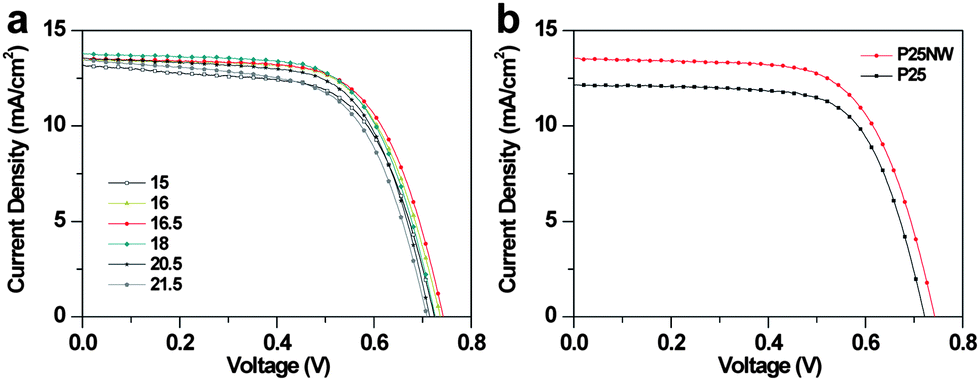 | ||
| Fig. 4 (a) J–V characteristics of the P25NW–DSCs at various film thicknesses. (b) J–V characteristics of the P25 and P25NW-DSCs at film thicknesses of 16.5 μm. | ||
| Thickness (μm) | Jsc (mA cm−2) | Voc (mV) | FF (%) | η (%) |
|---|---|---|---|---|
| 15 | 13.2 | 724.1 | 63.6 | 6.1 |
| 16 | 13.5 | 736.8 | 65.7 | 6.5 |
| 16.5 | 13.6 (12.2) | 741.8 (721.6) | 65.8 (68.1) | 6.6 (5.9) |
| 18 | 13.8 | 726.6 | 65.5 | 6.5 |
| 20.5 | 13.6 | 713.9 | 65.5 | 6.3 |
| 21.5 | 13.4 | 708.9 | 62.5 | 6.0 |
ηcc is generally determined by the IMPS and IMVS. Fig. 5a and b present the plots of the electron transport time (τt) and recombination lifetime (τr) measured by IMPS at short circuit and IMVS at open circuit, respectively. It is noticeable that the τt of the P25NW device is faster than that of the P25 device (Fig. 5a). The relatively faster electron transport appears to result from fewer interparticle junctions within the P25NW photoelectrode.36 The effective electron diffusion coefficient (Dn) can be estimated from the electron transport time using the following expression: Dn = L2/(2.35τt),37 where L is the film thickness. The Dn of P25NW cell was estimated to be 1.5 times larger than that of the P25 cell under 100 W m−2 illumination (Fig. 5c). The τr of the P25NW cell is longer than that of the P25 device over the whole light-intensity range (Fig. 5b). The increased τr is attributed to the presence of the relatively defect-free single crystalline NWs that have far fewer grain boundaries, which may cause the reduced electron trapping phenomena.30,31 The effective electron diffusion length (Ln) was obtained from Dn and τr using the relationship of Ln = (Dn × τr)1/2. The Ln of P25NW cell was approximately 1.5 times as thick as that of P25 device under a light intensity of 100 W m−2 (Fig. 5c). On the basis of the increased τr, improved photoelectron densities, n (n ∝ Jsc × τr),38 yielded a higher Voc (ref. 39) in the P25NW cell (Fig. 4b and Table 1).
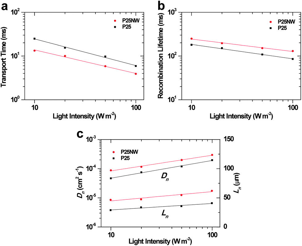 | ||
| Fig. 5 (a) The recombination lifetime plotted as a function of the incident light intensity. (b) The electron transport time plotted as a function of the incident light intensity. (c) The light-intensity-dependent electron diffusion coefficient (Dn) and length (Ln) of the DSCs based on the P25 and the P25NW films obtained under 535 nm LED illumination. | ||
ηcc can be estimated by the two values determined from the above IMPS and IMVS by adopting the following equation:40–42
 | (1) |
ηlh is commonly determined by light scattering of the films and the amount of adsorbed dye molecules. The light confinement effect is explained by the reflectance spectra. Fig. 6 shows reflectance spectra of the P25 and P25NW films at the same thickness (∼16.5 μm). For the P25NW sample, the reflectivity is increased in the whole visible wavelength region, unlike the P25 film. It is reasonable to expect that the NW-based DSCs are more beneficial in terms of photon management. The dye-loading capacity of the P25NW, 66.75 nmol−1 cm−2, was lower than that of the P25 films (81.26 nmol−1 cm−2). Therefore, ηlh may be mainly determined by light confinement effect. Consequently, it is reasonable to conclude that the observed higher photovoltaic performance of the P25NW cell is primarily due to the higher ηcc and ηlh of the NW–NP hybrid composite DSCs.
 | ||
| Fig. 6 Reflectance spectra of the P25 and P25NW films at film thicknesses of 16.5 μm. | ||
Conclusion
In summary, single crystalline rutile TiO2 NWs were directly grown on the commercial TiO2 NPs, P25 Degussa, using a simple solvothermal process. In detail, the NWs function not only as a highway for electron transport, but also as multiple light scatterers. On the contrary, the inlaid NPs compensate an insufficient surface area of the NWs. Consequently, the P25NW photoelectrode creates the tri-function of enhanced light confinement, high charge collection efficiency, and sufficient dye loading. As a result, maximum 6.6% efficiency was achieved by adopting the P25NW photoelectrode over the efficiency of the P25 device using only NPs with the same film thickness. We believe that the present hybridization can be extended to a variety of photo-electrochemical fields.Acknowledgements
This work was financially supported by the Basic Science Research Program (Grant no. 2012R1A1A2041628) through the National Research Foundation (NRF) of Korea funded by the Ministry of Education, Science and Technology.Notes and references
- D. Cummins, G. Boschloo, M. Ryan, D. Corr, S. N. Rao and D. Fitzmaurice, J. Phys. Chem. B, 2000, 104, 11449–11459 CrossRef CAS.
- K. Hashimoto, H. Irie and A. Fujishima, Jpn. J. Appl. Phys., 2005, 44, 8269–8285 CrossRef CAS.
- B. O'Regan and M. Grätzel, Nature, 1991, 353, 737–740 CrossRef CAS.
- S. K. Kim, G.-J. Choi, S. Y. Lee, M. Seo, S. W. Lee, J. H. Han, H.-S. Ahn, S. Han and C. S. Hwang, Adv. Mater., 2008, 20, 1429–1435 CrossRef CAS.
- J. Moon, J. A. Park, S. J. Lee, T. Zyung and I. D. Kim, Sens. Actuators, B, 2010, 149, 301–305 CrossRef CAS PubMed.
- N. Tétreault and M. Grätzel, Energy Environ. Sci., 2012, 5, 8506–8516 Search PubMed.
- J. Ferber and J. Luther, Sol. Energy Mater. Sol. Cells, 1998, 54, 265–275 CrossRef CAS.
- D. H. Chen, L. Cao, F. Z. Huang, P. Imperia, Y. B. Cheng and R. A. Caruso, J. Am. Chem. Soc., 2010, 132, 4438–4444 CrossRef CAS PubMed.
- J. H. Pan, X. Z. Wang, Q. Huang, C. Shen, Z. Y. Koh, Q. Wang, A. Engel and D. W. Bahnemann, Adv. Funct. Mater., 2013 DOI:10.1002/adfm.201300946.
- Y.-C. Park, E.-H. Kong, Y.-J. Chang, B.-G. Kum and H. M. Jang, Electrochim. Acta, 2011, 56, 7371–7376 CrossRef CAS PubMed.
- X. Feng, K. Zhu, A. J. Frank, C. A. Grimes and T. E. Mallouk, Angew. Chem., Int. Ed., 2012, 51, 2727–2730 CrossRef CAS PubMed.
- M. Adachi, Y. Murata, J. Takao, J. Jiu, M. Sakamoto and F. Wang, J. Am. Chem. Soc., 2004, 126, 14943–14949 CrossRef CAS PubMed.
- K. Zhu, N. R. Neale, A. Miedaner and A. J. Frank, Nano Lett., 2007, 7, 69–74 CrossRef CAS PubMed.
- J. G. Yu, J. J. Fan and K. L. Lv, Nanoscale, 2010, 2, 2144–2149 RSC.
- E.-H. Kong, Y.-J. Chang, Y.-C. Park, Y.-H. Yoon, H.-J. Park and H. M. Jang, Phys. Chem. Chem. Phys., 2012, 14, 4620–4625 RSC.
- M. Ye, C. Chen, M. Lv, D. Zheng, W. Guo and C. Lin, Nanoscale, 2013, 5, 6577–6583 RSC.
- L.-L. Li, C.-Y. Tsai, H.-P. Wu, C.-C. Chen and E. W.-G. Diau, J. Mater. Chem., 2010, 20, 2753–2758 RSC.
- D. Kuang, J. Brillet, P. Chen, M. Takata, S. Uchida, H. Miura, K. Sumioka, S. M. Zakeeruddin and M. Grätzel, ACS Nano, 2008, 2, 1113–1116 CrossRef CAS PubMed.
- D. Hwang, H. Lee, S.-Y. Jang, S. M. Jo, D. Kim, Y. Seo and D. Y. Kim, ACS Appl. Mater. Interfaces, 2011, 3, 2719–2725 CAS.
- W. Y. Cheng, J. R. Deka, Y. C. Chiang, A. Rogeau and S. Y. Lu, Chem. Mater., 2012, 24, 3255–3262 CrossRef CAS.
- X. J. Lu, F. Q. Huang, X. L. Mou, Y. M. Wang and F. F. Xu, Adv. Mater., 2010, 22, 3719–3722 CrossRef PubMed.
- B. Koo, J. Park, Y. Kim, S. H. Choi, Y. E. Sung and T. Hyeon, J. Phys. Chem. B, 2006, 110, 24318–24323 CrossRef CAS PubMed.
- G. Rothenberger, P. Comte and M. Grätzel, Sol. Energy Mater. Sol. Cells, 1999, 58, 321–336 CrossRef CAS.
- Q. Zhang, D. Myers, J. Lan, S. A. Jenekhe and G. Cao, Phys. Chem. Chem. Phys., 2012, 14, 14982–14998 RSC.
- D. Chen, F. Huang, Y.-B. Cheng and R. A. Caruso, Adv. Mater., 2009, 21, 2206–2210 CrossRef CAS.
- S. R. Gajjela, C. Yap and P. Balaya, J. Mater. Chem., 2012, 22, 10873–10882 RSC.
- Y.-C. Park, Y.-J. Chang, B.-G. Kum, E.-H. Kong, J. Y. Son, Y. S. Kwon, T. Park and H. M. Jang, J. Mater. Chem., 2011, 21, 9582–9586 RSC.
- Z. S. Wang, H. Kawauchi, T. Kashima and H. Arakawa, Coord. Chem. Rev., 2004, 248, 1381–1389 CrossRef CAS PubMed.
- B. Lee, D.-K. Hwang, P. Guo, S.-T. Ho, D. B. Buchholtz, C.-Y. Wang and R. P. H. Chang, J. Phys. Chem. B, 2010, 114, 14582–14591 CrossRef CAS PubMed.
- J. T. Jiu, S. Isoda, F. M. Wang and M. Adachi, J. Phys. Chem. B, 2006, 110, 2087–2092 CrossRef CAS PubMed.
- S. H. Kang, S. H. Choi, M. S. Kang, J. Y. Kim, H. S. Kim, T. Hyeon and Y. E. Sung, Adv. Mater., 2008, 20, 54–58 CrossRef CAS.
- X. G. Peng, L. Manna, W. D. Yang, J. Wickham, E. Scher, A. Kadavanich and A. P. Alivisatos, Nature, 2000, 404, 59–61 CrossRef CAS PubMed.
- A. S. Barnard and L. A. Curtiss, Nano Lett., 2005, 5, 1261–1266 CrossRef CAS.
- M. Adachi, Y. Murata, J. Takao, J. T. Jiu, M. Sakamoto and F. M. Wang, J. Am. Chem. Soc., 2004, 126, 14943–14949 CrossRef CAS PubMed.
- J. H. Pan, H. Dou, Z. Xiong, C. Xu, J. Ma and X. S. Zhao, J. Mater. Chem., 2010, 20, 4512–4528 RSC.
- B. H. Lee, M. Y. Song, S.-Y. Jang, S. M. Jo, S.-Y. Kwak and D. Y. Kim, J. Phys. Chem. C, 2009, 113, 21453–21457 CAS.
- J. van de Lagemaat and A. J. Frank, J. Phys. Chem. B, 2001, 105, 11194–11205 CrossRef CAS.
- G. Schlichthorl, S. Y. Huang, J. Sprague and A. J. Frank, J. Phys. Chem. B, 1997, 101, 8141–8155 CrossRef.
- A. J. Frank, N. Kopidakis and J. van de Lagemaat, Coord. Chem. Rev., 2004, 248, 1165–1179 CrossRef CAS PubMed.
- G. Schlichthörl, N. G. Park and A. J. Frank, J. Phys. Chem. B, 1999, 103, 782–791 CrossRef.
- L. Bertoluzzi and S. Ma, Phys. Chem. Chem. Phys., 2013, 15, 4283–4285 RSC.
- E.-H. Kong, J. Lim, Y.-J. Chang, Y.-H. Yoon, T. Park and H. M. Jang, Adv. Energy Mater., 2013, 3, 1344–1350 CrossRef CAS.
Footnote |
| † Electronic supplementary information (ESI) available: SEM images and J–V characteristics obtained from modified versions of P25NW. A TEM image of the P25NW (0.1 g). See DOI: 10.1039/c3ra44394a |
| This journal is © The Royal Society of Chemistry 2014 |