
 Open Access Article
 This Open Access Article is licensed under a
 Creative Commons Attribution 3.0 Unported Licence
Wire-shaped ultraviolet photodetectors based on a nanostructured NiO/ZnO coaxial p–n heterojunction via thermal oxidation and hydrothermal growth processes†
Yeong Hwan
Ko
,
Goli
Nagaraju
and
Jae Su
Yu
*
Department of Electronics and Radio Engineering, Kyung Hee University, 1732 Deogyeong-daero, Giheung-gu, Yongin-si, Gyeonggi-do 446-701, South Korea. E-mail: jsyu@khu.ac.kr; Fax: +82-31-206-2820; Tel: +82-31-201-3820
First published on 23rd December 2014
Abstract
We report the facile fabrication of wire-shaped ultraviolet photodetectors (WUPDs) by employing a nanostructured zinc oxide (ZnO)/nickel oxide (NiO) coaxial p–n heterojunction. The WUPD consists of a ZnO/NiO coaxial Ni wire and a twisted gold (Au) wire where the Ni and Au are used as the anode and cathode, respectively. For the coaxial p–n heterojunction, the NiO nanostructures (NSs) and the ZnO nanorods (NRs) are subsequently formed on the surface of Ni wire via thermal oxidation and hydrothermal growth processes. With an applied bias of −3.5 V, the WUPD exhibits good photoresponsivity of 7.37 A W−1 and an external quantum efficiency of 28.1% at an incident light wavelength of 325 nm. Under the UV illumination at a wavelength of 365 nm, the dark current and photocurrent are −3.97 × 10⁻⁷ and −8.47 × 10⁻⁶ A, respectively. For enhancing the photocurrent, the WUPD is threaded through a silver (Ag) coated glass tube which acts as a waveguide to concentrate the UV light of 365 nm on the WUPD. As a result, the photocurrent is significantly improved up to −1.56 × 10⁻⁵ A (i.e., 1.84 times) at the reverse bias of −3.5 V.
1 Introduction
Flexible miniature designs of devices have been in high demand for ubiquitous technologies in modern digital life with an increasing requirement for wearable, portable, multifunctional, and embedded electronic/optoelectronic systems.1–6 Accordingly, there has been a lot of effort to develop flexible and nano/micrometer-sized devices by employing nanomaterials and novel structures.1,7–9 Presently, basic two-dimensional (2D) materials such as graphene, molybdenum disulfide, gallium sulfide, and gallium telluride have been widely studied for the fabrication of photodetectors (PDs) with their excellent mechanical, electrical, and optical properties compared to bulk materials.10–13 However, some difficulty still exists in utilizing them for flexible and wearable devices. Typically, for 2D material-based flexible PDs and electronic devices, single- or few-layered 2D material sheets were prepared using scotch tape. Moreover, large-area 2D materials were successfully grown on rigid substrates by chemical vapor deposition. However, this process needs additional processes for safely transferring them to flexible substrates with connecting electrodes,14–17 which is productively and technologically complicated for the realization of practical device applications. Recently, wire-shaped and small-sized electronic and optoelectronic devices including supercapacitors, solar cells, and lithium-ion batteries have been developed with advanced designs for flexible and wearable applications because they are implemented by a facile fabrication process and exhibit promising device performances.18–22 Since carbon nanotubes (CNTs) were intensively studied as electrode materials, a lot of efforts have been focused on research for 1D microwire-based devices.19,23 The coaxial structures of CNTs were fabricated by drawing or twisting with functional materials such as semiconductors, electrochemicals, and photoanodes. For extension, multiple functional layers were coated on the overall surface of metal or steel microwires.24–27 These kinds of device structures have many advantages in terms of fabrication method and device performance. Industrial technologies associated with electronic textiles and clothes have been well developed for 1D microwire-based devices in a wide variety of fields. Also, the improved device efficiency can be expected with high flexibility, reduced weight, and low cost. Unfortunately, there are very few reports on the wire-shaped ultraviolet (UV) PDs.On the other hand, wide band-gap (Eg > 3.0 eV) semiconductor nanostructure-based UV PDs have achieved high photocurrent gain and good photoresponsivity thanks to their high quantum efficiency as well as large surface to volume ratio.28–31 Among various wide band-gap materials, zinc oxide (ZnO, Eg ∼ 3.37 eV) and nickel oxide (NiO, Eg ∼ 3.37 eV) have been widely used for n-type and p-type semiconductors, respectively, in optoelectronic applications.32,33 Particularly, the nanostructured ZnO/NiO p–n heterojunction can be prepared by a chemical route which is a simple and cost-effective process for scalable production without any high-vacuum system.34,35 However, the direct chemical synthesis of p–n heterojunctions has suffered from drawbacks such as poor crystallinity and imperfections.34 In this work, we have prepared coaxial ZnO/NiO nanostructures (NSs) as a p–n heterojunction, synthesized by thermal oxidation and hydrothermal growth processes, for wire-shaped ultraviolet photodetectors (WUPDs). The coaxial p–n heterojunction was successfully incorporated into the WUPDs with small size and flexibility like human hair. Additionally, the enhanced photocurrent was explored by threading the WUPDs into a silver (Ag) coated glass tube. This novel and simple design/fabrication of WUPDs can be expected to realize a scalable production by a technical assistance of well-developed textile technologies.
2 Experimental details
2.1 Preparation of samples
To obtain a nanostructured NiO/ZnO coaxial p–n heterojunction, the Ni wire (99.9%, Nilaco Corp., Japan) was first oxidized in a furnace at 750 °C for 1 h under an air atmosphere. Then, the NiO NS grown Ni wire was immersed into the ZnO seed solution for 3 h at room temperature. The seed solution was prepared by mixing 50 mL of ethanol and 100 mM of zinc acetate dehydrate at 80 °C with 0.75 mL of triethylamine. After drying at 100 °C for 3 h in an oven, the ZnO seed nanoparticle coated sample was immersed into the growth solution, prepared by dissolving 25 mM of zinc nitrate hydrate and 25 mM of hexamethylenetetramine. The growth solution was then heated at 90 °C for 3 h in an oven. After that, it was carefully removed and washed with flowing de-ionized water. For drying, the samples were placed in a furnace at 350 °C for 1 h. In order to form two electrodes, the Ni core was exposed by a simple mechanical scratching as an anode and the Au wire was twisted on the sample as a cathode. For the preparation of Ag coated glass tube, Pasteur pipette (Volac D810, John Poulten Ltd.) was plated with Ag by Tollen's reagent.2.2 Characterization
The morphological and structural properties were observed by using a FE-SEM (LEO SUPRA 55, Carl Zeiss) and a TEM (JEM 200CX, JEOL). The crystallinity was evaluated by the X-ray diffraction (XRD) measurement (M18XHF-SRA, Mac Science). The reflectance spectra were recorded by using a UV-vis-NIR spectrophotometer (Cary 5000, 102 Varian). The photoresponse characteristics of the WUPD were studied by using a semiconductor characterization system (Keithley 4200) with a tunable light source (TLS-300X, Newport Corp.) equipped with a 300 W xenon lamp. For rigorous coupled-wave analysis (RCWA) and finite-difference time-domain (FDTD) calculations, a commercial software (DiffractMOD and FullWave 3.1, Rsoft Design) was utilized.3 Results and discussion
A nanostructured ZnO/NiO coaxial p–n heterojunction was formed on the Ni wire (diameter: 100 μm) by thermal oxidation and subsequent hydrothermal synthesis. For the anode and cathode, the Ni and gold (Au) were contacted on the p-type NiO and n-type ZnO, respectively. As can be seen in the schematic diagram of Fig. 1a, the WUPD consists of a nanostructured ZnO/NiO coaxial Ni wire and a twisted Au wire (diameter: 20 μm). When photons are absorbed by the ZnO/NiO coaxial p–n heterojunction under UV illumination, electron–hole pairs are generated and they contribute to an induced photocurrent with a charge transport under reverse bias. In a typical process to manufacture wire-shaped devices, the core of coaxial wire was selectively exposed by etching, and then two metal contacts were made to the core/shell via a lithographic patterning.36,37 However, this needs complicated and accurate skills. To be more practical for applications, recently, a twisted electrode wire has been reported on dye-sensitized solar cells and electrochemical capacitors.20,38 Instead of metal patterning, the carbon nanotubes or metal wires were stably twisted together with active coaxial wires. In our design of the WUPDs, a thin Au wire is suitably twisted on the shell of coaxial Ni wire, which plays an important role in exposing a large active area for absorbing the UV light as well as collecting the diffused charge carriers from electron–hole generation. Fig. 1b shows the photographic image of the fabricated WUPD in comparison with a human hair. The WUPD exhibited a gentle curve of the twisted wire with a length of ∼ 5 cm. Since the WUPD is composed primarily of metal wires, it is physically suitable for flexible and bendable applications. To facilitate a connection of both the electrodes, the Au wire was twisted with an extra line and the Ni core was exposed at the end of coaxial wire by a simple mechanical scratching. In the macro view of the photographic image as shown in Fig. 1c, it is clearly observed that the Au electrode wire is spirally coiled around the ZnO/NiO coaxial Ni wire. Therefore, the Au is spontaneously contacted to the n-type ZnO.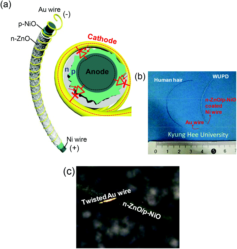 | ||
| Fig. 1 (a) Schematic diagram of the WUPD with a nanostructured ZnO/NiO coaxial p–n heterojunction and twisted Au wire, (b) photographic image of the fabricated WUPD in comparison with a human hair, and (c) micro view of photographic image of the WUPD. The ZnO/NiO coated Ni wire (diameter: 100 μm) was contacted with the twisted Au wire (diameter: 20 μm). | ||
To investigate the morphological features of the ZnO/NiO coaxial Ni wire, the schematic illustrations and their corresponding field-emission scanning electron microscope (FE-SEM) images are shown in Fig. 2. For a pure Ni wire, a commercially produced metal wire (purity: 99.9%) was employed. The Ni wire which is fabricated in a hot wire rolling process has smooth surface so that it was directly utilized for synthesizing the ZnO/NiO coaxial p–n heterojunction as shown in Fig. 2a. Then, the NiO NSs were grown on the Ni wire by a facile oxidation process. At 750 °C for 1 h under an air atmosphere, the NiO NSs were covered and distributed regularly over the whole surface of the Ni wire (ESI, Fig. S1†). The heating temperatures below 650 °C were not sufficient for growing the NiO NSs from the Ni wire. Above 750 °C, meanwhile, the size and surface roughness of NiO NSs were increased with increasing the temperature. As can be seen in the magnified FE-SEM image of Fig. 2b, the grown NiO NSs exhibited a very rough surface with various sizes of ∼85–580 nm. At the initial stage of thermal oxidation under the above conditions, the bulk Ni surface was formed into NiO shells by contacting with oxygen at high temperature and it transformed into a p-type semiconductor with Ni2+ vacancies.39 As the thermal oxidation further progressed, the NiO NSs were grown mainly by the cationic diffusion (that is, the Ni2+ ions are diffused outward through NiO shells) and the size of NiO was increased. After that, as shown in Fig. 2c, the ZnO NRs were integrated on the NiO NSs via a hydrothermal method for the coaxial p–n heterojunction. To densely and regularly grow the ZnO NRs, nanoparticles as seed layer were coated on the porous surface of the NiO NSs. Here, their sizes were approximately estimated to be between 7 and 35 nm (ESI, Fig. S2†). During the hydrothermal process, the seed nanoparticles serve as ZnO crystal nuclei sites and influence the size and density of ZnO NRs.40,41 The zinc hydroxide was anisotropically grown at the polar facet of the wurtzite crystal structure and it was converted into ZnO by dehydration. As can be seen in the magnified FE-SEM image in Fig. 2c, the ZnO NRs were distributed in a closely packed manner on the surface of the wire with a density of 108 μm−2, estimated as an average number of NRs in unit area. Their sizes and lengths were approximately 35–112 nm and 175–320 nm, respectively.
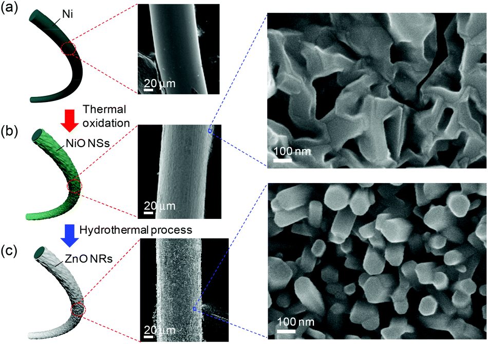 | ||
| Fig. 2 (a) Schematic diagram for the fabrication process of the nanostructured ZnO/NiO coaxial Ni wire by thermal oxidation and subsequent hydrothermal synthesis, and magnified FE-SEM images of (b) NiO NSs and (c) ZnO NRs. | ||
Fig. 3a shows the 2θ scan XRD patterns of the NiO NSs on Ni wire and the ZnO NRs grown on NiO NSs (i.e., ZnO NRs/NiO NSs) on Ni wire. To analyze the XRD patterns, the diffraction peaks were indexed by three JCPDS cards (Ni: 87-0712, NiO: 47-1049 and ZnO: 36-1451). For both the samples, the strong and sharp Ni peaks were commonly observed at 44.39, 51.98 and 76.13° corresponding to (111), (200), and (220) planes of a face-centered cubic structure, respectively. These high-intensity peaks indicate that pure Ni still remains intact at the core of the wire after the thermal oxidation and hydrothermal processes. Therefore, the Ni core can be readily used as the electrode by a simple mechanical scratching (ESI, Fig. S3†). The peaks located at 37.46, 43.41, 52.03 and 63.16° are related to the thermally grown NiO. Among them, several dominant peaks were indexed as NiO (111), (200) and (220) planes related to growth direction. During the thermal oxidation process, NiO nuclei were formed on the surface of Ni with adsorbed oxygen and they were grown along the unspecific direction, thus leading to a rough surface. For the ZnO NRs/NiO NSs on Ni wire, the dominant ZnO XRD peak for the (002) plane was clearly observed. This means that the ZnO NRs were mainly grown along the c-axis of the hexagonal wurtzite structure.42 Thus, the ZnO NRs tend to be perpendicularly aligned on the seed layer. In Fig. 3b, the transmission electron microscope (TEM) images and selected area electron diffraction (SAED) patterns of single NiO NS and single ZnO NR are shown. From the high-resolution TEM (HRTEM) image of both the samples for the marked region by a red circle, the lattice fringes were ordered and the lattice spacings of 0.24 and 0.52 nm were matched to the NiO (111) and ZnO (002) planes of XRD patterns. Also, the clear dot SAED patterns confirm that the ZnO NRs and NiO NSs have good crystallinities.
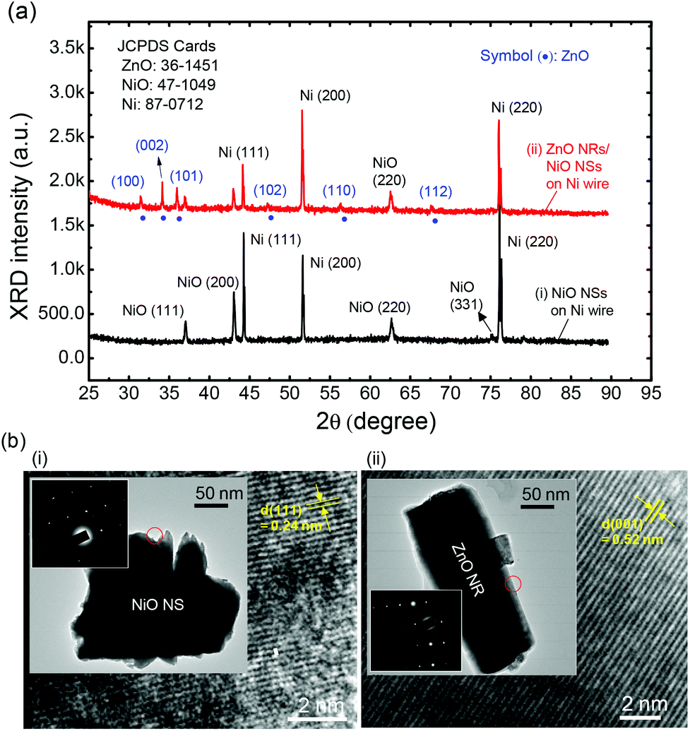 | ||
| Fig. 3 (a) 2θ scan XRD patterns of (i) the NiO NSs on Ni wire and (ii) the ZnO NRs grown on NiO NSs on Ni wire and (b) TEM and HRTEM images and SAED patterns of (i) single NiO NS and (ii) single ZnO NR. | ||
Fig. 4a shows the measured current–voltage (I–V) curves of the fabricated WUPD and the energy band diagram of the nanostructured NiO/ZnO p–n heterojunction. As the bias was swept from −5 to 5 V at room temperature in a dark box, the I–V curves exhibited a rectifying behavior. The corresponding energy band diagram is given by Anderson's model with material parameters of ZnO and NiO.43 When the reverse bias increases across the two electrodes, the depletion region becomes wider, inducing a high potential barrier at the coaxial p–n heterojunction of the nanostructured NiO/ZnO. Therefore, the carrier transport is suppressed along the high impedance path like an insulator. To characterize the photoresponse properties of the WUPD, the spectral responsivity (Rλ) was measured under a reverse bias of −3.5 V as shown in Fig. 4b. Here, the Rλ is presented as a ratio of photocurrent to light intensity at a specific wavelength in unit of A W−1. Therefore, it can be expressed by a simple relationship of Rλ = ΔI × p(λ)−1 × A−1, where ΔI, p(λ), and A are the photoexcited current, the light intensity as a function of wavelength, and the effective area, respectively. The effective area was estimated as a half surface area of cylinder for WUPDs as shown in the inset of Fig. 4c. When the incident wavelength was decreased from 380 nm, the Rλ gradually increased and the maximum peak of 7.39 A W−1 was obtained at ∼310 nm. Meanwhile, the relatively low value of 2.05 A W−1 was observed at 365 nm. To calculate the external quantum efficiency (EQE) of the WUPD, the equation of EQE = 1240 × Rλ × λ−1 was used. The EQE values of 28.1 and 6.95% were obtained at the incident light wavelengths of 325 and 365 nm, respectively. Considering the absorption band edges of NiO (310 nm) and ZnO (365 nm), it can be explained by the fact that the incident light of 365 nm is absorbed mainly by ZnO NRs and some photocurrent is induced by charge carrier generation. To estimate the photoabsorption properties of ZnO/NiO in WUPD, we measured absorbance spectra of the ZnO NRs and NiO NSs with ethanol because it is very difficult to directly characterize the absorption of the thin wire. For preparation, the ZnO NRs and NiO NRs powders were obtained by scratching the sample and were then mixed with ethanol. As shown in the absorbance spectra (ESI, Fig. S4†), the EQE spectrum could be compared to the shape of the absorbance curve for the ZnO NRs and NiO NSs. Owing to trap levels and imperfections of the grown metal oxides, the difference between the EQE and absorbance spectra was also observed. For practical applications such as flammability tests, detection of ozone hole, and sterilization monitoring, it is desirable that the photoresponsivity should be high at the absorption edge of 365 nm. Fig. 4c shows the measured I–V curves of the WUPD in the dark and under the illumination of 2.5 mW cm−2 using a 365 nm UV light-emitting diode (LED). At −5 V, the dark current and photocurrent were −4.55 and −18.27 μA, respectively. As shown in the inset of Fig. 4c, the WUPD absorbs small portions of photons because a directly illuminated light faces mainly the front of thin wire. If the UV light is guided towards the overall surface of the WUPD, the photocurrent can be sufficiently enhanced. Thus, the WUPD was threaded in the Ag coated glass tube. This will be explained in detail with theoretical and experimental results later. Fig. 4d shows the photoresponse characteristics of the WUPD with a reverse bias of −3.5 V under the on/off switching of UV LED. In order to examine a repeatability of this WUPD, the results of repeated measurements are shown in the ESI (Fig. S5†). As the 365 nm light was turned-on, the photocurrent dramatically increased from 2 to 9.8 μA. After the light was turned-off, the WUPD clearly revealed the transient characteristics with a reset time (τ) of 18.1 s. Here, the τ was obtained by the relationship of I = (Imax – Idark)e−t/τ, where Imax and Idark are the maximum and dark currents, respectively. These photoresponse properties are similar to the previous results for ZnO NS-based PDs. Water molecules and ambient oxygen at the ZnO contribute to the adsorption and photodesorption. However, a somewhat slow decay process was observed due to the re-adsorption process.44 Comparison of the characteristics of different UV photodetectors is shown in Table 1.
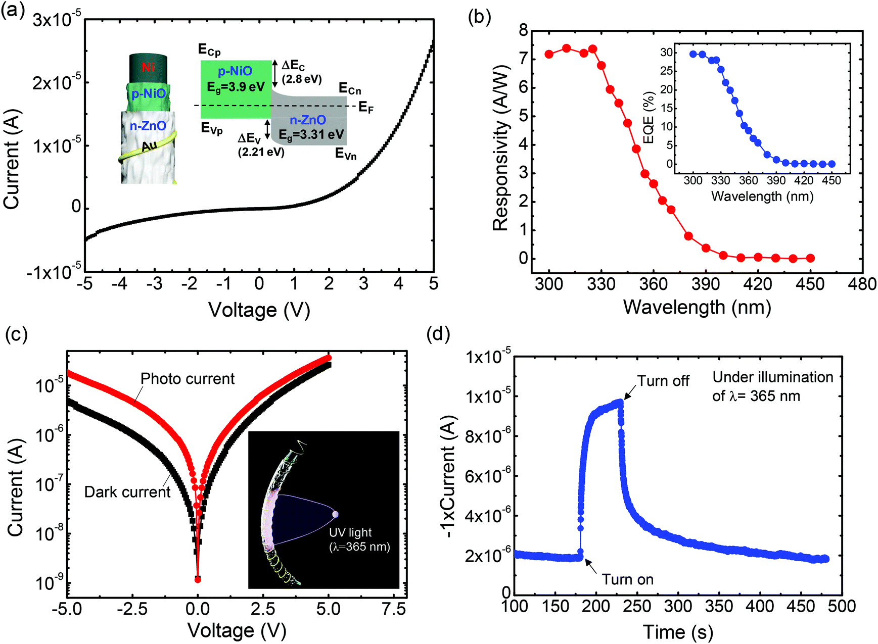 | ||
| Fig. 4 (a) I–V curve of the WUPD with a nanostructured NiO/ZnO coaxial p–n heterojunction, (b) Rλ and EQE of the WUPD under a reverse bias of −3.5 V, (c) I–V curves of the WUPD in the dark and under the illumination of 2.5 mW cm−2 using a 365 nm UV LED, and (d) photoresponse characteristics of the WUPD at reverse bias of −3.5 V under the on/off switching of the same UV LED. The energy band diagram of the nanostructured NiO/ZnO coaxial p–n heterojunction is shown in the inset of (a). | ||
As previously explained, the WUPD was threaded into an Ag coated glass tube as illustrated in Fig. 5a. By using Tollen's test, the thin Ag film was coated on the glass tube with a thickness of ∼115 nm (ESI, Fig. S6†). Since the internal diameter of the glass tube is about 0.5 mm, the relatively thin WUPD can be easily placed inside. To investigate the reflection characteristics, the Ag film was coated on a glass slide under the same conditions as shown in the photographic image. Fig. 5b shows the contour plot of reflectance spectra as a function of thickness of Ag film. This result was calculated using a RCWA method. In the UV region, the reflectance was largely decreased with decreasing the wavelength from 370 to 300 nm. Above 100 nm of thickness of Ag film, the reflectance was higher than 80% at a wavelength of 365 nm. At this wavelength, it is possible to concentrate them on the WUPD owing to the high internal reflection at the inside of the Ag coated glass tube. Fig. 5c shows the measured (solid lines) and calculated (dash lines) reflectance, transmittance and absorptance spectra of the Ag coated glass slide in the wavelength region from 300 to 550 nm. The theoretical results by RCWA calculations well agreed with the experimental results. As the wavelength was decreased from 400 to 300 nm, the transmittance was increased and the reflectance was decreased significantly because the difference of refractive indices between Ag and glass is smaller for shorter UV wavelengths (i.e., the refractive index of Ag is 1.49 at 300 nm of wavelength). For the wavelength of 365 nm, the Ag coated glass had a high reflectance of 82.88%. In order to estimate the light propagation properties of 365 nm in the Ag coated glass tube, the FDTD simulation was carried out.
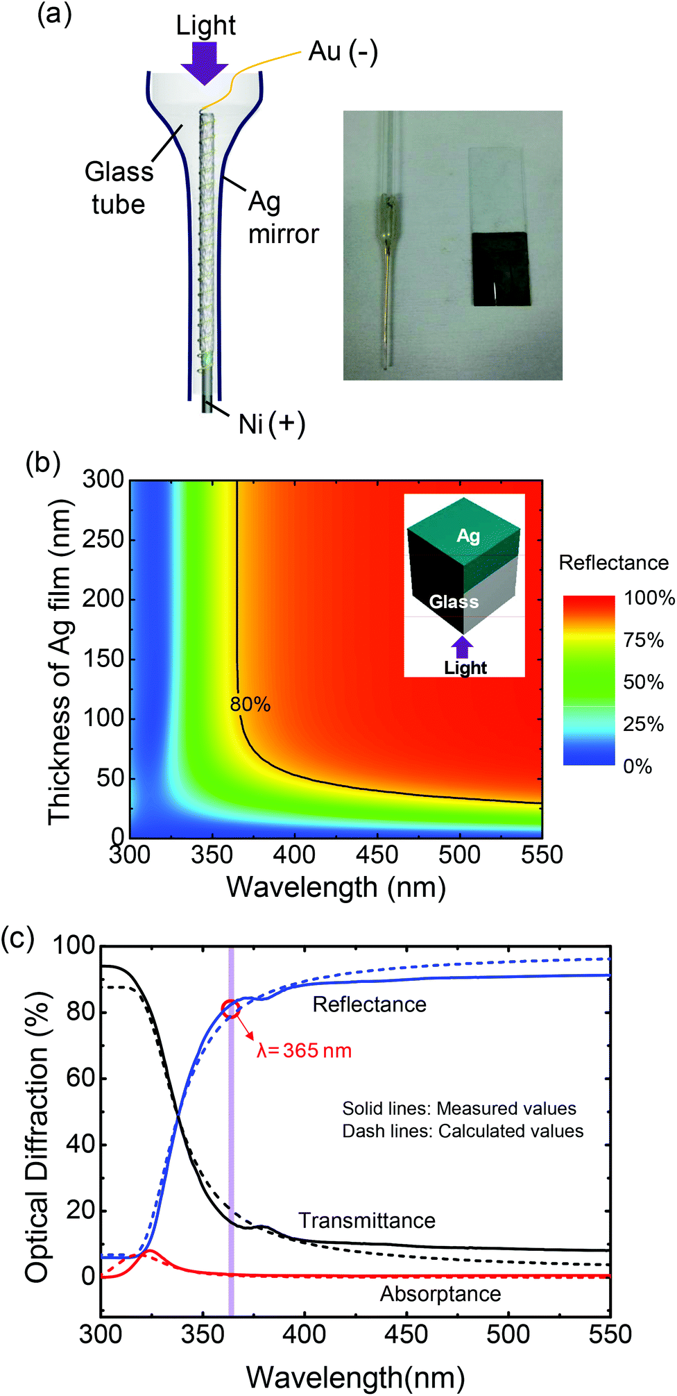 | ||
| Fig. 5 (a) Schematic illustration of the threaded WUPD into an Ag coated glass tube for enhancing the photocurrent at 365 nm of incident light, (b) contour plot of reflectance spectra as a function of thickness of Ag film using RCWA calculations, and (c) measured (solid lines) and calculated (dash lines) reflectance, transmittance, and absorptance spectra of the Ag coated glass. | ||
Fig. 6a shows the side view of the calculated electric field distribution of the light propagating into the Ag coated glass. The cross-sectional view of the calculated electric field distribution is also shown (ESI, Fig. S7†). Herein, it was assumed that the incident plan wave propagates with a Gaussian beam profile at 365 nm of wavelength. Between the glass and Ag media, as shown in the contour plot, the light reflection occurred dominantly at the inside of the glass tube. Additionally, the light gradually converged to the center as it propagated through the tapered region, concentrating the UV light of 365 nm on the WUPD. In order to estimate the quantitative properties of absorbed light intensity, the average of the squared absolute value for calculated electric fields along the lateral direction from Fig. 6a was obtained (Fig. 6b). At the center of the lateral position, the averaged value for the Ag coated glass tube was enhanced by 2.45 times as compared to the averaged value for no Ag coated glass tube. Fig. 6c shows the measured I–V curves of the WUPD with and without an Ag coated glass tube under the illumination at the wavelength of 365 nm. Also, the photographic image of the threaded WUPD into the Ag coated glass tube is shown in the inset. When the bias was swept from zero to −5 V, the photocurrent was enhanced for the WUPD with the Ag coated glass tube. At −3.5 V, the photocurrent was considerably increased by 1.84 times from −8.47 to −15.65 μA, which is well consistent with the quantitative properties of absorbed light intensity of Fig. 6b. This enhancement is mainly attributed to the increase in the illuminated surface area of WUPD and the concentrated UV light, as theoretically investigated by FDTD simulations. The Ag coated glass tube enables the creation of the UV light guide into the high-reflective inner surface of the cylindrical WUPD. Considering the metallic coating with high reflectivity, it is sufficient to propagate the light waves (around 365 nm) through the Ag coated glass tube without distinct losses. This novel design of the threaded WUPD with an Ag coated glass tube can provide an effective waveguide structure to improve the device performance in various miniature wire-shaped optoelectronic applications.
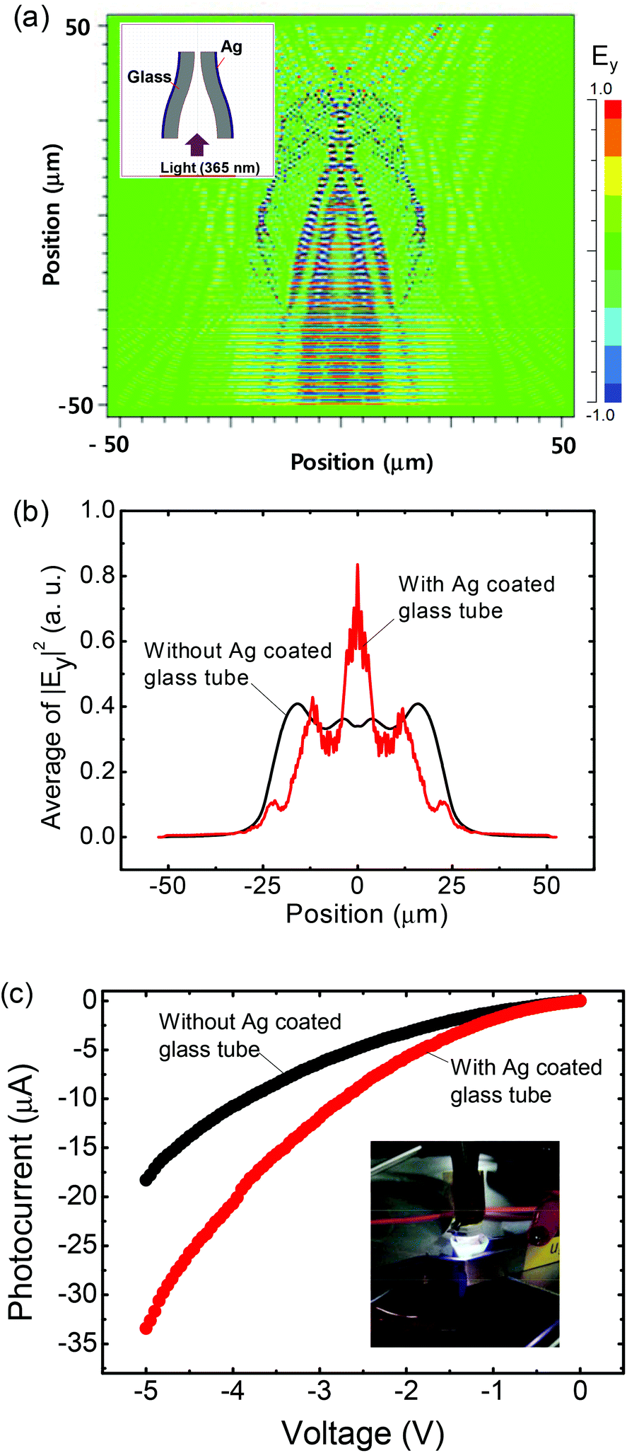 | ||
| Fig. 6 (a) Side view of the FDTD calculated electric field distribution of the light propagating into the Ag coated glass at 365 nm of wavelength, (b) average of the squared absolute value for calculated electric fields along the lateral direction from (a), and (c) I–V curves of the WUPDs with and without Ag coated glass tube under the illumination at wavelength of 365 nm. The inset also shows the photographic image of the threaded WUPD into the Ag coated glass tube. | ||
4 Conclusions
The WUPD based on the nanostructured ZnO/NiO coaxial p–n heterojunction was fabricated by the thermal oxidation and hydrothermal growth processes and their photoresponse properties including Rλ, EQE and transient time were characterized. The NiO NSs and ZnO NRs were coated on a Ni wire and they exhibited good crystallinities. Furthermore, this novel structure can be expected to realize small-sized and flexible devices like a human hair. For applying the reverse bias of −3.5 V to the WUPD, the 7.37 A W−1 (28.1%) and 2.05 A W−1 (6.95%) of Rλ (EQE) were obtained at the incident light wavelengths of 325 and 365 nm, respectively. To enhance the photocurrent at 365 nm, in terms of absorption edge, the thin WUPD was placed in the high-reflective Ag (82.88%) coated glass tube. The UV light of 365 nm can be concentrated on the inner surface of the threaded WUPD, thus enhancing the photocurrent. The proposed WUPD, combined with the aid of the UV light guide, can be attractive for use in various fields, including flexible UV sensors, embedded optoelectronic devices, and multifunctional applications.Acknowledgements
This research was supported by Basic Science Research Program through the National Research Foundation of Korea (NRF) funded by the Ministry of Science, ICT and Future Planning (no. 2013-010037 and no. 2013-068407).Notes and references
- G. Zheng, Y. Cui, E. Karabulut, L. Wågberg, H. Zhu and L. Hu, MRS Bull., 2013, 38, 320 CrossRef CAS.
- H. Ko, R. Kapadia, K. Takei, T. Takahashi, X. Zhang and A. Javey, Nanotechnol., 2012, 23, 344001 CrossRef PubMed.
- X. Wang, W. Song, B. Liu, G. Chen, D. Chen, C. Zhou and G. Shen, Adv. Funct. Mater., 2013, 23, 1202 CrossRef CAS.
- A. Vaseashta and D. Dimova-Malinovska, Sci. Technol. Adv. Mater., 2005, 6, 312 CrossRef CAS PubMed.
- Y. Xie, M. Gong, T. A. Shastry, J. Lohrman, M. C. Hersam and S. Ren, Adv. Mater., 2013, 25, 3433 CrossRef CAS PubMed.
- C. Yan, J. Wang, X. Wang, W. Kang, M. Cui, C. Y. Foo and P. S. Lee, Adv. Mater., 2014, 26, 943 CrossRef CAS PubMed.
- Y. Liu, R. Cheng, L. Liao, H. Zhou, J. Bai, G. Liu, L. Liu, Y. Huang and X. Duan, Nat. Commun., 2011, 2, 579 CrossRef PubMed.
- L. Vj, J. Oh, A. P. Nayak, A. M. Katzenmeyer, K. H. Gilchrist, S. Grego, N. P. Kobayashi, S. Y. Wang, A. A. Talin, N. K. Dhar and M. S. Islam, IEEE J. Sel. Top. Quantum Electron., 2011, 17, 1002 CrossRef.
- C. Pang, C. Lee and K. Y. Suh, J. Appl. Polym. Sci., 2013, 130, 1429 CrossRef CAS.
- Z. Sun, T. Liao, Y. Dou, S. M. Hwang, M.-S. Park, L. Jiang, J. H. Kim and S. X. Dou, Nat. Commun., 2014, 5, 3813 CAS.
- P. Hu, J. Zhang, M. Yoon, X.-F. Qiao, X. Zhang, W. Feng, P. Tan, W. Zheng, J. Liu, X. Wang, J. C. Idrobo, D. B. Geohegan and K. Xiao, Nano Res., 2014, 7, 694 CrossRef CAS.
- P. Hu, L. Wang, M. Yoon, J. Zhang, W. Feng, X. Wang, Z. Wen, J. C. Idrobo, Y. Miyamoto, D. B. Geohegan and K. Xiao, Nano Lett., 2013, 13, 1649 CAS.
- Z. Sun and H. Chang, ACS Nano, 2014, 8, 4133 CrossRef CAS PubMed.
- Z. Yin, H. Li, H. Li, L. Jiang, Y. Shi, Y. Sun, G. Lu, Q. Zhang, X. Chen and H. Zhang, ACS Nano, 2012, 6, 74 CrossRef CAS PubMed.
- C. H. Liu, Y. C. Chang, T. B. Norris and Z. Zhong, Nat. Nanotechnol., 2014, 9, 273 CrossRef CAS PubMed.
- W. Zhang, C. P. Chuu, J. K. Huang, C. H. Chen, M. L. Tsai, Y. H. Chang, C. T. Liang, Y. Z. Chen, Y. L. Chueh, J. H. He, M. Y. Chou and L. J. Li, Sci. Rep., 2014, 4, 3826 Search PubMed.
- O. Lopez-Sanchez, D. Lembke, M. Kayci, A. Radenovic and A. Kis, Nat. Nanotechnol., 2013, 8, 497 CrossRef CAS PubMed.
- Z. Cai, L. Li, J. Ren, L. Qiu, H. Lin and H. Peng, J. Mater. Chem. A, 2013, 1, 258 CAS.
- X. Chen, L. Qiu, J. Ren, G. Guan, H. Lin, Z. Zhang, P. Chen, Y. Wang and H. Peng, Adv. Mater., 2013, 25, 6436 CrossRef CAS PubMed.
- X. Fan, Z. Z. Chu, F. Z. Wang, C. Zhang, L. Chen, Y. W. Tang and D. C. Zou, Adv. Mater., 2008, 20, 592 CrossRef CAS.
- T. Chen, L. Qiu, Z. Cai, F. Gong, Z. Yang, Z. Wang and H. Peng, Nano Lett., 2012, 12, 2568 CrossRef CAS PubMed.
- J. Bae, M. K. Song, Y. J. Park, J. M. Kim, M. Liu and Z. L. Wang, Angew. Chem., Int. Ed., 2011, 50, 1683 CrossRef CAS PubMed.
- W. Guo, C. Liu, F. Zhao, X. Sun, Z. Yang, T. Chen, X. Chen, L. Qiu, X. Hu and H. Peng, Adv. Mater., 2012, 24, 5379 CrossRef CAS PubMed.
- S. Zhang, C. Ji, Z. Bian, P. Yu, L. Zhang, D. Liu, E. Shi, Y. Shang, H. Peng, Q. Cheng, D. Wang, C. Huang and A. Cao, ACS Nano, 2012, 6, 7191 CrossRef CAS PubMed.
- D. Liu, Y. Li, S. Zhao, A. Cao, C. Zhang, Z. Liu, Z. Bian, Z. Liu and C. Huang, RSC Adv., 2013, 3, 13720 RSC.
- Y. Liu, M. Li, H. Wang, J. Zheng, H. Xu, Q. Ye and H. Shen, J. Phys. D: Appl. Phys., 2010, 43, 205103 CrossRef.
- Z. Zhang, Z. Yang, Z. Wu, G. Guan, S. Pan, Y. Zhang, H. Li, J. Deng, B. Sun and H. Peng, Adv. Energy Mater., 2014, 4, 1301750 Search PubMed.
- L. Sang, M. Liao and M. Sumiya, Sensors, 2013, 13, 10482 CrossRef CAS PubMed.
- E. Monroy, F. Omnès and F. Calle, Semicond. Sci. Technol., 2003, 18, R33 CrossRef CAS.
- A. BenMoussa, A. Soltani, U. Schühle, K. Haenen, Y. M. Chong, W. J. Zhang, R. Dahal, J. Y. Lin, H. X. Jiang, H. A. Barkad, B. BenMoussa, D. Bolsee, C. Hermans, U. Kroth, C. Laubis, V. Mortet, J. C. De Jaeger, B. Giordanengo, M. Richter, F. Scholze and J. F. Hochedez, Diamond Relat. Mater., 2009, 18, 860 CrossRef CAS PubMed.
- C. Yan, N. Singh and P. S. Lee, Appl. Phys. Lett., 2010, 96, 053108 CrossRef PubMed.
- K. Liu, M. Sakurai and M. Aono, Sensors, 2010, 10, 8604 CrossRef CAS PubMed.
- B. Sasi and K. G. Gopchandran, Nanotechnol., 2007, 18, 115613 CrossRef.
- A. Chrissanthopoulos, S. Baskoutas, N. Bouropoulos, V. Dracopoulos, P. Poulopoulos and S. N. Yannopoulos, Photon. Nanostruct. Fundam. Appl., 2011, 9, 132 CrossRef PubMed.
- W. Dai, X. Pan, S. Chen, C. Chen, Z. Wen, H. Zhang and Z. Ye, J. Mater. Chem. C, 2014, 2, 4606 RSC.
- B. Tian, X. Zheng, T. J. Kempa, Y. Fang, N. Yu, G. Yu, J. Huang and C. M. Lieber, Nature, 2007, 449, 885 CrossRef CAS PubMed.
- Z. Zhang, X. Chen, P. Chen, G. Guan, L. Qiu, H. Lin, Z. Yang, W. Bai, Y. Luo and H. Peng, Adv. Mater., 2014, 26, 466 CrossRef CAS PubMed.
- J. Ren, L. Li, C. Chen, X. Chen, Z. Cai, L. Qiu, Y. Wang, X. Zhu and H. Peng, Adv. Mater., 2013, 25, 1155 CrossRef CAS PubMed.
- K. Koga and M. Hirasawa, Nanotechnology, 2013, 24, 375602 CrossRef PubMed.
- N. S. Ridhuan, K. A. Razak, Z. Lockman and A. Abdul Aziz, PLoS One, 2012, 7, e50405 CAS.
- W. Y. Wu, C. C. Yeh and J. M. Ting, J. Am. Ceram. Soc., 2009, 92, 2718 CrossRef CAS PubMed.
- S. Xu, C. Lao, B. Weintraub and Z. L. Wang, J. Mater. Res., 2011, 23, 2072 CrossRef.
- Y. I. Alivov, J. E. Van Nostrand, D. C. Look, M. V. Chukichev and B. M. Ataev, Appl. Phys. Lett., 2003, 83, 2943 CrossRef CAS PubMed.
- K. Hasan, N. H. Alvi, J. Lu, O. Nur and M. Willander, Nanoscale Res. Lett., 2011, 6, 348 CrossRef PubMed.
- N. Park, K. Sun, Z. Sun, Y. Jing and D. Wang, J. Mater. Chem. C, 2013, 1, 7333 RSC.
- D. Jiang, J. Qin, X. Zhang, Z. Bai and D. Shen, Mater. Sci. Eng., B, 2011, 176, 736 CrossRef CAS PubMed.
- F. Guo, B. Yang, Y. Yuan, Z. Xiao, Q. Dong, Y. Bi and J. Huang, Nat. Nanotechnol., 2012, 7, 798 CrossRef CAS PubMed.
Footnote |
| † Electronic supplementary information (ESI) available. See DOI: 10.1039/c4nr06662f |
| This journal is © The Royal Society of Chemistry 2015 |