
 Open Access Article
 This Open Access Article is licensed under a
 Creative Commons Attribution 3.0 Unported Licence
Probing planar defects in nanoparticle superlattices by 3D small-angle electron diffraction tomography and real space imaging†
Arnaud
Mayence
,
Dong
Wang‡
,
German
Salazar-Alvarez
 ,
Peter
Oleynikov
and
Lennart
Bergström
*
,
Peter
Oleynikov
and
Lennart
Bergström
*
Arrhenius Laboratory, Department of Materials and Environmental Chemistry, Stockholm University, Stockholm, Sweden. E-mail: lennart.bergstrom@mmk.su.se
First published on 17th September 2014
Abstract
We demonstrate how the acquisition and processing of 3D electron diffraction data can be extended to characterize structural features on the mesoscale, and show how lattice distortions in superlattices of self-assembled spherical Pd nanoparticles can be quantified by three-dimensional small-angle electron diffraction tomography (3D SA-EDT). Transmission electron microscopy real space imaging and 3D SA-EDT reveal a high density of stacking faults that was related to a competition between fcc and hcp arrangements during assembly. Information on the orientation of the stacking faults was used to make analogies between planar defects in the superlattices and Shockley partial dislocations in metallic systems.
Introduction
The structural diversity of single- and multiple-component nanoparticle superlattices1–6 is rapidly expanding and the ability to tune the electronic, optical and magnetic properties by the composition, size, and shape of the nanoparticles and their packing arrangements is attracting great interest.7–11 For instance, thin films of binary PbTe/Ag2 nanoparticle superlattices can show a high p-type conductivity,12 whereas planar iron oxide (γ-Fe2O3) nanoparticle assemblies display a 2D to 3D crossover of the magnetic properties that depend on the layer thickness.13 However, while the structural features are important, it is well known that the functionalities and performances of most materials are strongly influenced by their defects. This is also true for self-assembled colloidal crystals, exemplified by how planar defects14 (e.g. stacking faults) influence the photonic band gap structure, and how anisotropic strain in fcc photonic crystals breaks the selection rules for scattering resulting in a shift of the absorption peak.15Nanoparticle superlattices can be fabricated and assembled into different packing arrangements that are controlled by the morphology, interactions, and sizes of the nanoparticles, as well as the assembly conditions.16–20 While the packing arrangements of nanoparticle superlattices have been extensively investigated,21–25 studies that characterize and quantify defects in the arrays are sparse. Korgel and coworkers26 identified dislocations and quantified lattice distortions in binary nanoparticle superlattices of Fe3O4 and Au nanoparticles by grazing-incidence small-angle X-ray scattering (GISAXS) and electron microscopy. Talapin and coworkers27 identified and classified defects in crystalline and quasi-crystalline binary nanoparticle assemblies by TEM real space imaging. More recently, Disch et al.28 quantified the stacking fault concentration in assemblies of anisotropic nanoparticles by a combination of SEM and GISAXS.
3D electron crystallography encompasses novel approaches to study and solve crystal structures of challenging materials.29–31 Three-dimensional electron diffraction tomography (3D EDT) was successfully utilized to retrieve three-dimensional diffraction data and solve crystal structures on the atomic scale.32 We recently demonstrated that it is a robust and powerful method to identify and solve the structure of single nanocrystals.33 In contrast to conventional real space electron tomography, 3D EDT is less sensitive to specimen drift and the selected-area diffraction mode helps to minimize the electron dose the material is exposed to.
In this work, we show that 3D EDT, operating in the small-angle diffraction mode, can be used to study mesoscopic structures, e.g. 3D packing arrangements and lattice distortions in nanoparticle superlattices. TEM real space imaging (2D projection) and three-dimensional small-angle electron diffraction tomography (3D SA-EDT) have been combined to investigate defects in self-assembled superlattices of spherical palladium (Pd) nanoparticles. We show that the Pd nanoparticle superlattices display a high density of stacking faults that is related to the competition between the two densest ways to pack spheres, namely face-centered cubic (fcc) and hexagonal closed-packed (hcp) arrangements, and discuss the similarities to metallic systems. Lattice distortions in nanoparticle superlattices could be quantified by 3D SA-EDT, and we discuss how they are related to the symmetry breaking during assembly.
Experimental
Synthesis and self-assembly of Pd nanoparticles
Monodisperse spherical Pd nanoparticles were synthesized using a modified hot injection strategy.34 In a typical synthesis, 0.25 mmol palladium acetylacetonate (Pd(acac)2) and 0.3 mmol oleic acid were dissolved in 1 ml trioctylphosphine under vigorous stirring for one hour in a glove box, which yielded a bright yellow solution of the precursor. The precursor was rapidly injected into a vigorously stirred mixture of 19.27 g 1-octadecene and 390 mg 1,2-hexadecanediol (Sigma Aldrich 90%) pre-heated at 120 °C under argon protection. The solution was heated up to 316 °C at 3 °C min−1 heating rate followed by a reflux for 30 min to complete the synthesis. After synthesis, the flask was left under argon protection to cool down to room temperature. Nanoparticle purification was achieved by dilution/flocculation cycles using ethanol as the non-solvent, and toluene as the solvent. The final sample was dispersed in toluene for storage.The nanoparticle superlattices were produced by a controlled destabilization strategy35 where ethanol slowly diffuses into a dilute dispersion of Pd nanoparticles in toluene with a concentration of 1.3 mg Pd ml−1. Small aliquots of the dispersion were retrieved over a period of 24–72 hours and deposited onto TEM carbon coated grids. Typically, micrometer-sized facetted Pd nanoparticle superlattices are obtained over a period of time exceeding 72 hours (see ESI,† Fig. S1).
Characterization
Results and discussion
Real space imaging and 3D SA-EDT reconstruction were performed on nanoparticle superlattices thinner than 100 nm (3–10 layers of packed nanoparticles) that were obtained by retrieving small aliquots of the Pd nanoparticle dispersion during the first 24 hours of ethanol induced destabilisation. The TEM images in Fig. 1 show that the Pd nanoparticles assemble into a highly ordered close-packed arrangement with the surfactant-capped Pd spheres separated from each other by ∼2.0 nm. The 3D SA-EDT volume reconstruction (Fig. 1d–f) can be indexed either as a hcp lattice or as a fcc lattice, with unit cell dimensions of a = b = 7.9 nm and c = 12.0 nm, or a = 11.2 nm, respectively. The measured unit cell axial ratio, c/a ∼1.53, deviates by ∼7% from the ideal value of the hcp arrangement (∼1.63), suggesting a slight contraction of the lattice perpendicular to the substrate. Indeed, previous investigations have also observed lattice distortions perpendicular to the substrate and related this effect to the stresses induced by solvent removal.26,36 The 3D SA-EDT data set shows relatively sharp spots when viewed along the [001]hcp direction (Fig. 1d) unlike the substantial diffuse streaking observed when viewed along the [−110]hcp direction (Fig. 1e), suggesting that the nanoparticle superlattice contains a large number of stacking faults that propagate along the chcp-axis.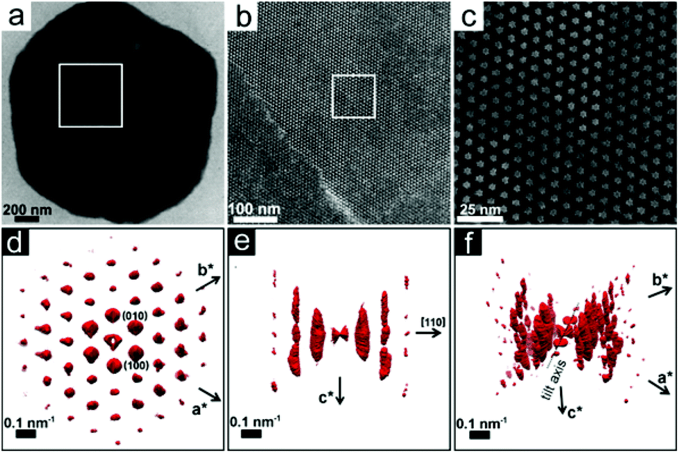 | ||
| Fig. 1 TEM bright-field images along [001]hcp and 3D SA-EDT volume reconstruction of a Pd nanoparticle superlattice. (a) Low magnification image. (b) Intermediate magnification from the area tagged in (a). (c) High magnification image from the area tagged in (b). 3D SA-EDT volume reconstruction of the array shown in (a) projected along; (d) [001]hcp, (e) [–110]hcp and (f) arbitrary crystallographic orientation. | ||
Fig. 2a shows that a Pd nanoparticle superlattice can contain a high concentration of stacking faults, consisting of a stacking sequence alternation of the nanoparticle close-packed planes, as outlined by the zigzag path traced in Fig. 2a. The stacking faults are running parallel to the substrate, along either the [001]hcp or the [111]fcc direction. The TEM image in Fig. 2b shows that the array is composed of nanoparticles with a hard core diameter of ∼5.3 nm, which is smaller than the mean diameter of the synthesized nanoparticles (6.1 nm). This difference may be related to local size segregation/fractionation during self-assembly as suggested in previous studies on polydisperse hard spheres.37,38 Interestingly, the 3D SA-EDT volume reconstruction (Fig. 2c–e) of the nanoparticle superlattice suggests a monoclinically distorted close-packed arrangement with unit cell parameters of a = 5.5 nm, b = 6.9 nm, c = 13.2 nm and α = 90°, β = 90° and γ = 115°. The analysis of the 3D SA-EDT data sets and TEM images also shows that the separation distance between the individual surfactant-capped nanoparticles can vary significantly from one superlattice to another. In fact, the 3D SA-EDT data set shown in Fig. 2 reveals that the inorganic cores of the Pd nanoparticles are almost in contact with each other (∼0.2 nm separation), suggesting that the ethanol destabilization process may promote desorption of the surfactants from the Pd surface.
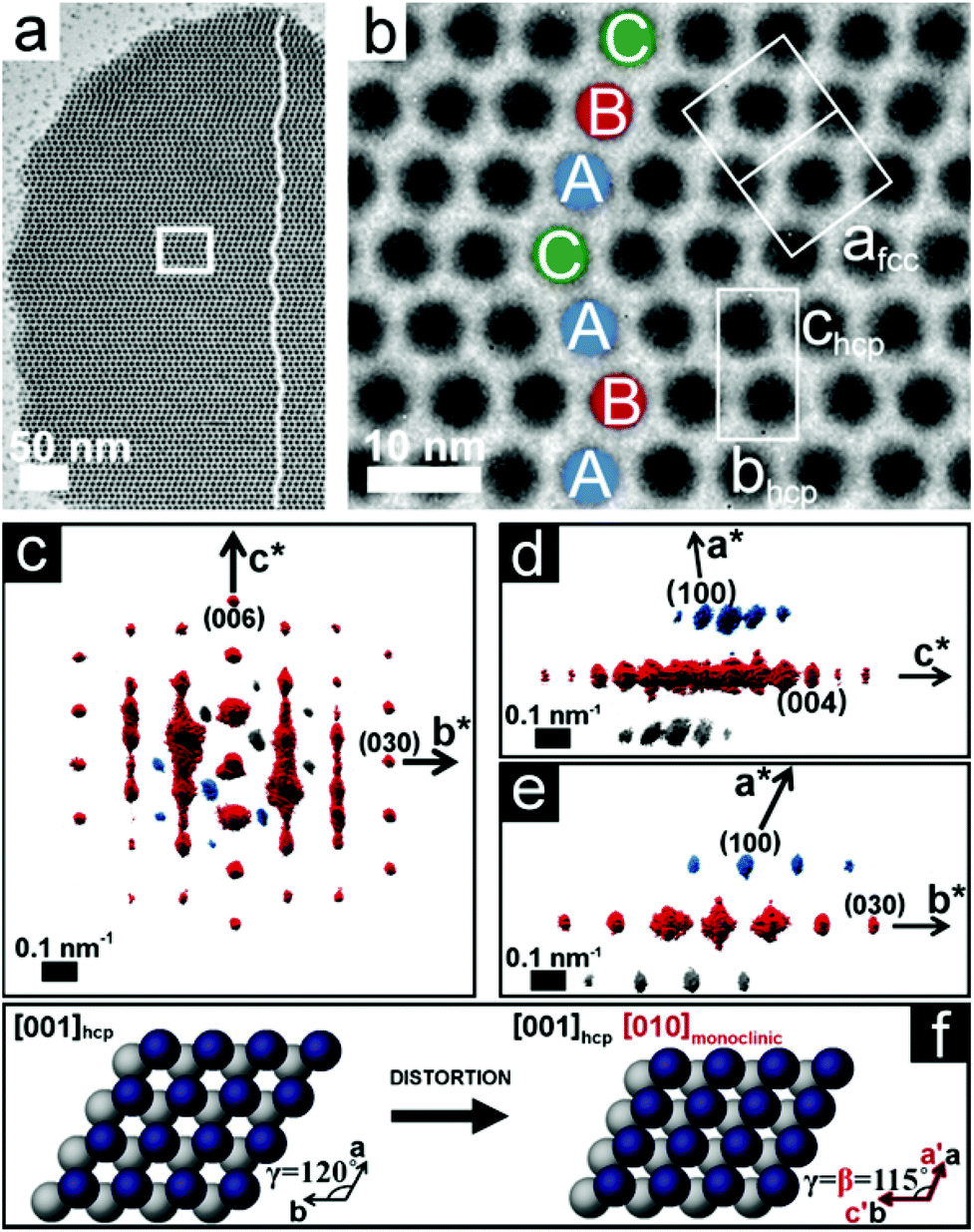 | ||
| Fig. 2 TEM bright-field images along [100]hcp, 3D SA-EDT volume reconstruction, and crystallographic models of a Pd nanoparticle superlattice assembled into a monoclinically distorted close-packed arrangement. (a) Image with zigzag features corresponding to stacking faults running (traced by lines) along the close-packed planes of the nanoparticle superlattice. (b) Magnified image of the area tagged in (a) revealing stacking faults. The sequence alternation of the nanoparticle close-packed planes is described using A, B, and C symbols in blue, red and green respectively. The two unit cell projections of the close-packed systems, i.e. fcc and hcp lattices, are outlined with their respective lattice constants. 3D SA-EDT reciprocal space reconstruction of the superlattice projected along: (c) [100]hcp; (d) [010]hcp; and (e) [001]hcp. (f) Crystallographic model projected parallel to the substrate (along [001]hcp) depicting the lattice distortion occurring in the array shown in (a). The monoclinic lattice axes are drawn in red. | ||
The comparison of the experimental 3D SA-EDT volume of the nanoparticle superlattice with the simulated 3D reciprocal volume reconstruction data set of an ideal hcp arrangement has been used to quantify the deviations from an ideal close-packed arrangement (space group: P63/mmc) (see ESI,† Fig. S5–7). We found that the monoclinic distortion, outlined in Fig. 2f, results in a decrease of the hexagonal basal plane angle of 5° and a lattice contraction of 20% along [100]hcp.
Fig. 3 gives further evidence of the hcp and fcc competition during assembly of spherical Pd nanoparticles. We have compared two nanoparticle superlattices where the (001)fcc facet dominates as shown in Fig. 3a and c. The TEM image in Fig. 3c shows that one of the superlattices displays distinct line defects with a regular spacing of ∼15–25 nm. These features are related to slanted (out-of-plane) stacking faults oriented at an angle of 54.7° (angle between [111]fcc and [001]fcc directions) with respect to the normal direction, [001]fcc. The stacking sequence alternation occurs at every third to fifth close-packed nanoparticle layer. Hence, the defect-rich nanoparticle superlattice consists of an fcc (red spheres) packing arrangement interrupted by hcp (blue spheres) subdomains as modelled on insets (see Fig. 3a and c). The small-angle electron diffraction patterns (SA-DPs) of the two superlattices shown in Fig. 3b and d correspond to a two-dimensional orthogonal unit cell with equal lengths of the a and b reciprocal vectors. However, the SA-DP in Fig. 3d exhibits additional diffuse scattering features near the Bragg reflections that are related to the stacking faults in the nanoparticle superlattices.
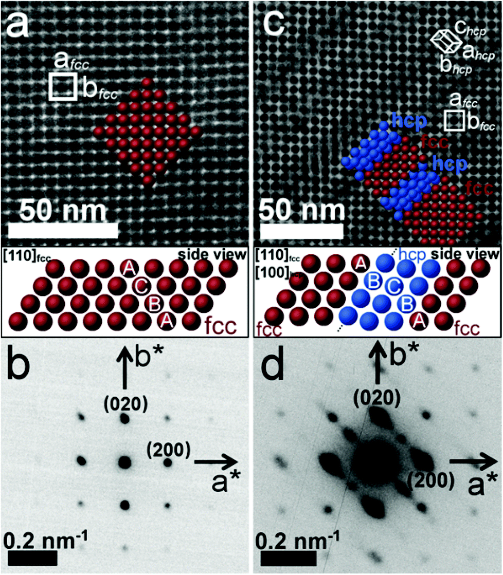 | ||
| Fig. 3 Slanted stacking faults in Pd nanoparticle superlattices. TEM bright-field images, crystallographic models and SA-DPs of Pd nanoparticle superlattices along [001]fcc: (a, b) with and (c, d) without planar defects. The crystallographic models viewed from the side, along [110]fcc, are provided below each images; the blue and red spheres depict hcp and fcc domains, respectively. | ||
Occassionally, the Pd nanoparticle superlattices exhibit multiple stacking fault directions; two in-plane (Fig. 4a), and a combination of in-plane and out-of-plane (Fig. 4b) directions. For example, Fig. 4b shows a nanoparticle superlattice oriented along [110]fcc where one stacking fault propagates along the substrate (zigzag traced line) while another is slanted at an angle of 35.2° between the (110)fcc and (111)fcc planes. While stacking faults clearly dominate in the Pd nanoparticle superlattices prepared by the interfacial destabilization technique, we also observe other imperfections, e.g. interstitial defects and grain boundaries, as shown in Fig. S8–11.† More complex defect-rich structures may also occur, as exemplified by a 5-fold twinned superlattice in Fig. 4c.
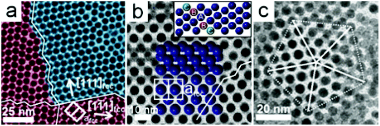 | ||
| Fig. 4 TEM bright-field images of Pd nanoparticle superlattices containing multiple stacking fault directions. (a) In-plane stacking faults running along two directions (traced by zigzag lines); (b) in-plane stacking fault (traced by zigzag line) and out-of-plane stacking faults outlined by crystallographic models. The 2D crystallographic models of the nanoparticles packing are provided along two projections, and the model inset shows the side view of the nanoparticles packing. (c) Example of 5-fold twinned nanoparticle array. | ||
It is well established that monodisperse spheres can assemble into two possible, but equally dense, close-packed arrangements; cubic close-packed (ccp), also known as face-centered cubic (fcc), and hexagonal close-packed (hcp) where the sequences of the close-packed planes are (⋯ABCABC⋯) and (⋯ABABAB⋯), respectively. For ideal hard spheres, the fcc lattice is the most thermodynamically favored packing but the free-energy difference between the two structures is very small (of the order of 10−3kBT per sphere).39–42 Previous reports on nanoparticle superlattices have indeed shown that spherical nanoparticles can assemble into both fcc and hcp arrangements.18,43,44
In this study, we found that stacking faults consisting of alternating fcc and hcp subdomains are the predominent defects. Indeed, very few of the superlattices are void of planar defects, and stacking faults are observed regardless of the preferential growth orientation of the self-assembled superlattices. The stacking faults can be characterized as a Shockley partial dislocation along the <112>fcc direction; a type of planar defect commonly found in close-packed metal structures45–47 and noble-gas clusters.48,49 The stacking faults observed in the nanoparticle superlattices are usually running along one unique direction over the whole array as shown in Fig. 2a. This is characteristic of an hcp system, depicted in Fig. 5a that permits only a single propagation direction, [001]hcp, of the stacking faults. On the other hand, the cubic symmetry of a fcc lattice allows four different and equally probable stacking directions, as shown in Fig. 5b. Therefore, stacking faults running along two different directions occur when the fcc packing sequence (⋯ABCABC⋯) is disrupted along two different {111} planes, e.g. the two in-plane stacking fault directions shown in Fig. 4a.
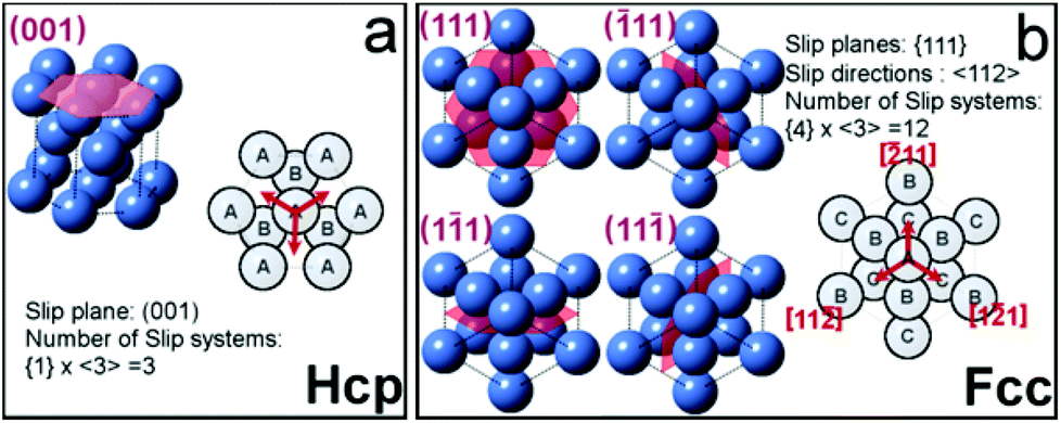 | ||
| Fig. 5 Crystallographic models of close-packed arrangements and their respective slip systems. (a) The hcp system with a single slip plane; (001). (b) The fcc system contains 12 independent slip systems, and 4 different slip planes; (111), (−111), (1−11) and (11−1). The red vectors depict the slip directions of the close-packed plane in both structures. | ||
However, it should be noted that the investigated nanoparticle superlattices rarely show multiple stacking fault directions, probably because this would significantly locally disrupt the close-packing and reduce the nanoparticle coordination number.
The stacking fault energy in solids can have an influence on the mechanical properties, where materials with a high concentration of stacking faults can be stronger compared to more defect-free materials, demonstrated e.g. in magnesium alloys.50 Therefore, it would be interesting to investigate the mechanical properties of defect-rich (e.g. having a high concentration of stacking faults) nanoparticle superlattices.
Conclusions
In summary, we have shown how a combination of transmission electron microscopy techniques, direct imaging and three-dimensional small-angle electron diffraction tomography (3D SA-EDT), can be successfully utilized to identify defects and quantify lattice distortion in nanoparticle superlattices. The superlattices exhibit a high concentration of stacking faults that were related to a competition between hcp and fcc arrangements, and analogies to close-packed metallic systems and solid noble gases were made. Further development of the 3D SA-EDT technique will open up opportunities to characterize and solve the 3D structures for a wide range of mesoscopic materials including electron beam sensitive samples, e.g. biopolymers, proteins and self-assembled organic structures.Acknowledgements
This work was financed by the Knut and Alice Wallenberg (KAW) Foundation through the project 3DEM-NATUR, and the Swedish Research Council (VR). The Knut and Alice Wallenberg (KAW) Foundation is acknowledged for providing the electron microscopy facilities.References
- D. V. Talapin, E. V. Shevchenko, M. I. Bodnarchuk, X. Ye, J. Chen and C. B. Murray, Nature, 2009, 461, 964–967 CrossRef CAS PubMed.
- A. Dong, J. Chen, P. M. Vora, J. M. Kikkawa and C. B. Murray, Nature, 2010, 466, 474–477 CrossRef CAS PubMed.
- E. V. Shevchenko, D. V. Talapin, N. A. Kotov, S. O'Brien and C. B. Murray, Nature, 2006, 439, 55–59 CrossRef CAS PubMed.
- K. Miszta, J. de Graaf, G. Bertoni, D. Dorfs, R. Brescia, S. Marras, L. Ceseracciu, R. Cingolani, R. van Roij, M. Dijkstra and L. Manna, Nat. Mater., 2011, 10, 872–876 CrossRef CAS PubMed.
- R. J. Macfarlane, B. Lee, M. R. Jones, N. Harris, G. C. Schatz and C. A. Mirkin, Science, 2011, 334, 204–208 CrossRef CAS PubMed.
- A. Dong, X. Ye, J. Chen and C. B. Murray, Nano Lett., 2011, 11, 1804–1809 CrossRef CAS PubMed.
- J. Chen, A. Dong, J. Cai, X. Ye, Y. Kang, J. M. Kikkawa and C. B. Murray, Nano Lett., 2010, 10, 5103–5108 CrossRef CAS PubMed.
- S. Sun, C. B. Murray, D. Weller, L. Folks and A. Moser, Science, 2000, 287, 1989–1992 CrossRef CAS PubMed.
- D. Parker, I. Lisiecki, C. Salzemann and M. Pileni, J. Phys. Chem. C, 2007, 111, 12632–12638 CAS.
- J. M. Luther, M. Law, Q. Song, C. L. Perkins, M. C. Beard and A. J. Nozik, ACS Nano, 2008, 2, 271–280 CrossRef CAS PubMed.
- J. Dintinger, S. Mühlig, C. Rockstuhl and T. Scharf, Opt. Mater. Express, 2012, 2, 269–278 CrossRef CAS.
- J. J. Urban, D. V. Talapin, E. V. Shevchenko, C. R. Kagan and C. B. Murray, Nat. Mater., 2007, 6, 115–121 CrossRef CAS PubMed.
- B. Faure, E. Wetterskog, K. Gunnarsson, E. Josten, R. P. Hermann, T. Brückel, J. W. Andreasen, F. Meneau, M. Meyer, A. Lyubartsev, L. Bergström, G. Salazar-Alvarez and P. Svedlindh, Nanoscale, 2013, 5, 953–960 RSC.
- Y. A. Vlasov, V. N. Astratov, A. V. Baryshev, A. A. Kaplyanskii, O. Z. Karimov and M. F. Limonov, Phys. Rev. E: Stat. Phys., Plasmas, Fluids, Relat. Interdiscip. Top., 2000, 61, 5784–5793 CrossRef CAS.
- A. Kontogeorgos, D. R. E. Snoswell, C. E. Finlayson, J. J. Baumberg, P. Spahn and G. P. Hellmann, Phys. Rev. Lett., 2010, 105, 233909 CrossRef PubMed.
- A. M. Kalsin, M. Fialkowski, M. Paszewski, S. K. Smoukov, K. J. M. Bishop and B. A. Grzybowski, Science, 2006, 312, 420–424 CrossRef CAS PubMed.
- E. V. Shevchenko, D. V. Talapin, C. B. Murray and S. O'Brien, J. Am. Chem. Soc., 2006, 128, 3620–3637 CrossRef CAS PubMed.
- D. V. Talapin, E. V. Shevchenko, C. B. Murray, A. V. Titov and P. Kral, Nano Lett., 2007, 7, 1213–1219 CrossRef CAS PubMed.
- Y. Min, M. Akbulut, K. Kristiansen, Y. Golan and J. Israelachvili, Nat. Mater., 2008, 7, 527–538 CrossRef CAS PubMed.
- H. Portalès, N. Goubet, S. Sirotkin, E. Duval, A. Mermet, P.-A. Albouy and M.-P. Pileni, Nano Lett., 2012, 12, 5292–5298 CrossRef PubMed.
- M. P. Boneschanscher, W. H. Evers, W. Qi, J. D. Meeldijk, M. Dijkstra and D. Vanmaekelbergh, Nano Lett., 2013, 13, 1312–1316 CrossRef CAS PubMed.
- H. Friedrich, C. J. Gommes, K. Overgaag, J. D. Meeldijk, W. H. Evers, B. de Nijs, M. P. Boneschanscher, P. E. de Jongh, A. J. Verkleij, K. P. de Jong, A. van Blaaderen and D. Vanmaekelbergh, Nano Lett., 2009, 9, 2719–2724 CrossRef CAS PubMed.
- I. Florea, A. Demortière, C. Petit, H. Bulou, C. Hirlimann and O. Ersen, ACS Nano, 2012, 6, 2574–2581 CrossRef CAS PubMed.
- P. Simon, E. Rosseeva, I. A. Baburin, L. Liebscher, S. G. Hickey, R. Cardoso-Gil, A. Eychmüller, R. Kniep and W. Carrillo-Cabrera, Angew. Chem., Int. Ed., 2012, 51, 10776–10781 CrossRef CAS PubMed.
- S. Bals, M. Casavola, M. A. van Huis, S. Van Aert, K. J. Batenburg, G. Van Tendeloo and D. Vanmaekelbergh, Nano Lett., 2011, 11, 3420–3424 CrossRef CAS PubMed.
- D. K. Smith, B. Goodfellow, D.-M. Smilgies and B. A. Korgel, J. Am. Chem. Soc., 2009, 131, 3281–3290 CrossRef CAS PubMed.
- M. I. Bodnarchuk, E. V. Shevchenko and D. V. Talapin, J. Am. Chem. Soc., 2011, 133, 20837–20849 CrossRef CAS PubMed.
- S. Disch, E. Wetterskog, R. P. Hermann, D. Korolkov, P. Busch, P. Boesecke, O. Lyon, U. Vainio, G. Salazar-Alvarez, L. Bergström and T. Brückel, Nanoscale, 2013, 5, 3969–3975 RSC.
- Y. Li, L. Zhang, A. Torres-Pardo, J. M. González-Calbet, Y. Ma, P. Oleynikov, O. Terasaki, S. Asahina, M. Shima, D. Cha, L. Zhao, K. Takanabe, J. Kubota and K. Domen, Nat. Commun., 2013, 4, 2566 Search PubMed.
- E. Mugnaioli and U. Kolb, Microporous Mesoporous Mater., 2013, 166, 93–101 CrossRef CAS.
- Y. Zhang, J. Su, H. Furukawa, Y. Yun, F. Gándara, A. Duong, X. Zou and O. M. Yaghi, J. Am. Chem. Soc., 2013, 135, 16336–16339 CrossRef CAS PubMed.
- M. Gemmi and P. Oleynikov, Z. Kristallogr. - Cryst. Mater., 2013, 228, 51–58 CrossRef CAS.
- A. Mayence, J. R. G. Navarro, Y. Ma, O. Terasaki, L. Bergström and P. Oleynikov, Inorg. Chem., 2014, 53, 5067–5072 CrossRef CAS PubMed.
- Y. Hou, H. Kondoh, T. Kogure and T. Ohta, Chem. Mater., 2004, 16, 5149–5152 CrossRef CAS.
- D. V. Talapin, E. V. Shevchenko, A. Kornowski, N. Gaponik, M. Haase, A. L. Rogach and H. Weller, Adv. Mater., 2001, 13, 1868 CrossRef CAS.
- M. Klotz, P. Albouy, A. Ayral, C. Ménager, D. Grosso, A. Van der Lee, V. Cabuil, F. Babonneau and C. Guizard, Chem. Mater., 2000, 12, 1721–1728 CrossRef CAS.
- D. Kofke and P. Bolhuis, Phys. Rev. E: Stat., Nonlinear, Soft Matter Phys., 1999, 59, 618–622 CrossRef CAS.
- H. J. Schöpe, G. Bryant and W. van Megen, J. Chem. Phys., 2007, 127, 084505 CrossRef PubMed.
- S. Pronk and D. Frenkel, J. Chem. Phys., 1999, 110, 4589–4592 CrossRef CAS.
- P. G. Bolhuis, D. Frenkel, S. Mau and D. A. Huse, Nature, 1997, 388, 235–236 CrossRef CAS.
- A. Bruce, N. Wilding and G. Ackland, Phys. Rev. Lett., 1997, 79, 3002–3005 CrossRef CAS.
- S.-C. Mau and D. Huse, Phys. Rev. E: Stat., Nonlinear, Soft Matter Phys., 1999, 59, 4396–4401 CrossRef CAS.
- A.-I. Henry, A. Courty, M.-P. Pileni, P.-A. Albouy and J. Israelachvili, Nano Lett., 2008, 8, 2000–2005 CrossRef CAS PubMed.
- C. B. Murray, C. R. Kagan and M. G. Bawendi, Science, 1995, 270, 1335–1338 CAS.
- D. Hull and D. J. Bacon, Introduction to Dislocations, Butterworth-Heinemann, 5th edn, 2011 Search PubMed.
- J. Urban, Cryst. Res. Technol., 1998, 33, 1009–1024 CrossRef CAS.
- A. Kelly and K. M. Knowles, Crystallography and Crystal Defects, John Wiley & Sons, Ltd, Chichester, UK, 2nd edn, 2012, vol. 331 Search PubMed.
- B. W. van de Waal, Phys. Rev. Lett., 1996, 76, 1083–1086 CrossRef CAS PubMed.
- M.-F. de Feraudy and G. Torchet, J. Cryst. Growth, 2000, 217, 449–457 CrossRef CAS.
- W. W. Jian, G. M. Cheng, W. Z. Xu, H. Yuan, M. H. Tsai, Q. D. Wang, C. C. Koch, Y. T. Zhu and S. N. Mathaudhu, Mater. Res. Lett., 2013, 1, 61–66 CrossRef CAS.
Footnotes |
| † Electronic supplementary information (ESI) available: Material characterization, simulated and experimental 3D reciprocal volume reconstruction and TEM bright-field images of nanoparticle superlattices. See DOI: 10.1039/c4nr04156a |
| ‡ Present address: Department of Chemical Engineering, Northeast Dianli University, Jilin, China. |
| This journal is © The Royal Society of Chemistry 2014 |