
 Open Access Article
 This Open Access Article is licensed under a
 Creative Commons Attribution 3.0 Unported Licence
Tungsten oxide nanorod growth by pulsed laser deposition: influence of substrate and process conditions
Peng
Huang†
a,
M. Mazhar
Ali Kalyar‡
a,
Richard F.
Webster
b,
David
Cherns
b and
Michael N. R.
Ashfold
*a
aSchool of Chemistry, University of Bristol, Bristol, BS8 1TS, UK. E-mail: mike.ashfold@bris.ac.uk; Tel: +44 (0)117 9288312
bSchool of Physics, University of Bristol, Tyndall Avenue, Bristol, BS8 1TL, UK
First published on 16th September 2014
Abstract
Tungsten oxide nanorods (NRs) have been grown on W, Ta and Cu substrates following 193 nm pulsed laser ablation of a WO3 target in a low background pressure of oxygen. The deposited materials were analysed by scanning and (high resolution) transmission electron microscopy (HRTEM), selected area electron diffraction (SAED), X-ray diffraction, Raman and X-ray photoemission spectroscopy, and tested for field emission. In each case, HRTEM analysis shows NR growth along the [100] direction, and clear stacking faults running along this direction (which are also revealed by streaking in the SAED pattern perpendicular to the growth axis). The NR composition in each case is thus determined as sub-stoichiometric WO3−δ, but the NR morphologies are very different. NRs grown on W or Ta are short (hundreds of nm in length) and have a uniform cross-section, whereas those grown on a Cu substrate are typically an order of magnitude larger, tapered, and display a branched, dendritic microstructure. Only these latter NRs give significant field emission.
1. Introduction
Tungsten oxide (WOx, x ≤ 3), an n-type semiconducting metal oxide with band gap Eg ∼ 2.6–3.0 eV, attracts interest by virtue of its rich crystallography, its many attractive properties and the diversity of routes by which it can be prepared in low-dimensional nanostructured form.1 Chromism (i.e. colour change in response to external stimuli such as voltage, reducing gases, heat and/or light)2,3 is arguably its most distinctive property, with real or potential applications in smart windows, flat panel displays, optical memory and read–write–erase devices, but other reported applications of tungsten oxide films include photocatalysis,4 water splitting,5 gas sensing applications6,7 and dye sensitized solar cells.8WOx structures are typically based on slightly distorted variants of the ReO3 cubic crystal structure, with each metal atom lying at the centre of an octahedron of O atoms. Tunnels of varying shapes and sizes may thus arise. Stoichiometric WO3 itself can exist in several different polymorphs formed by appropriate tilting and/or rotation of the constituent WO6 octahedra without relaxing the requirement of corner sharing. As with other perovskite-based transition metal oxides, however, tungsten oxide also readily tolerates oxygen vacancies, which can coalesce to form defects (shear planes). Such WOx (x ≤ 3) structures necessarily consist of both edge- and corner-shared octahedra, and many stable sub-stoichiometric structures have been characterised.1,9
Relative to the bulk material, nanostructured WOx samples will display an increased surface-to-volume ratio and may thus be expected to offer enhanced performance with respect to properties that are sensitive to, for example, modifications to the surface energies or possible quantum confinement effects.1 The detailed properties of low-dimensional materials are sensitive to many factors, however, including chemical composition, thermochemical (phase) stability, crystal structure, surface morphology, porosity, etc., so the exploration of different routes to forming nanostructured WOx remains a very active area of research. Demonstrated growth methods include both solution-based (hydrothermal methods, acid-bath, sol–gel, electrodeposition, etc.)1,10–14 and vapour phase approaches (e.g. physical vapour deposition, thermal evaporation, sputtering, etc.),1,15,16 with post-annealing in oxygen or air offering further possibilities for tuning the O content, phase, and crystallinity of the as-grown material.
Pulsed laser deposition (PLD) has also been used to produce WOx films,17–23 including films composed of nanorods (NRs) on quartz substrates.24,25 PLD offers the advantage of relatively slow growth, in a clean and dry environment. In the case of ZnO, for example, PLD constitutes a catalyst-free route to forming arrays of high quality, aligned NRs, with controllable diameter and aspect ratio.26,27 Here, we show that PLD also offers a route to forming WOx NRs on a range of metal substrates (tungsten, tantalum and copper), and explore the sensitivity of the deposition process to conditions like substrate temperature, O2 pressure, and incident fluence. The present study confirms that WOx NRs can be grown on each of these substrates with just subtle changes in process conditions, but also reveals that the crystallinity and morphology of the resulting NRs is sensitively dependent on process conditions (particularly the choice of substrate).
2. Experimental
WOx NRs were deposited on W (Goodfellow, as rolled, 99.95% purity), Ta (Testbourne, rolled bright annealed, 99.99% purity) and Cu (Goodfellow, annealed, 99.9% purity) foil substrates using apparatus that has been described previously.26 The deposition chamber was evacuated using a rotary-backed turbomolecular pump, yielding a typical base pressure of ∼1 × 10⁻⁶ Torr. The output of an ArF excimer laser (Coherent, COMPex Pro 102, 193 nm, 10 Hz repetition rate) was focused onto a rotating WO3 target (Testbourne, hot pressed polycrystalline sample, 99.95% purity) at a 45° incident angle, yielding an incident fluence F = 6–10 J cm−2. The resulting plume of ablated material propagates roughly symmetrically about the target surface normal and impinges on the substrate, which is positioned at a distance D = 70 mm from the target. Substrates were ultrasonically cleaned in acetone, then washed with 99.98% ethanol, dried in air, and attached to a 250 W tungsten halogen quartz bulb (used as a heater, and capable of maintaining the substrate temperature, Tsub, within 10 °C of any selected value in the range 25 ≤ Tsub ≤ 700 °C) for the duration of the deposition, t. The chamber is designed to allow back-filling with a steady (10 sccm) flow of oxygen, hence providing for a background pressure in the range 0 ≤ pO2 ≤ 100 mTorr during the PLD stage. ‘Base’ conditions were taken to correspond to pO2 = 10 mTorr.The as-grown WOx samples were characterized by field emission scanning electron microscopy (FE-SEM, JEOL6300LV), transmission electron microscopy (TEM, JEOL 1200EX), high resolution transmission electron microscopy (HRTEM, JEOL 2010), selected area electron diffraction (SAED, Philips EM430 TEM), X-ray diffraction (XRD, Bruker AXS D8 Advance powder diffractometer with Cu Kα radiation), Raman spectroscopy (Renishaw InVia spectrometer, 632.8 nm excitation), X-ray photoemission spectroscopy (XPS, Kratos Axis Ultra DLD photoelectron spectrometer with a monochromatic Al Kα source (1486.6 eV)), and their field emission properties investigated.
3. Results and discussion
Observations and analyses of WOx NR samples grown on W, Ta and Cu substrates are presented and discussed in sequence. Experimental parameters (F, Tsub, t and pO2) were varied in each case, but with particular emphasis on identifying process conditions that led to the richest nanostructure rather than seeking to maintain constancy across the three families of depositions. The various substrates were cleaned, successively, in acetone then ethanol in an ultrasonic bath, then dried with compressed air, but otherwise used as supplied. Only reflections attributable to the bare metal were identifiable by XRD, but we recognize that each substrate must be covered with a thin surface oxide layer from the very start of the PLD process.3.1. Growth on W substrates
Heating a W substrate28 (or a W film on a Si substrate29) in an oxygen-containing atmosphere is a known route to forming WOx NRs. Environmental TEM studies of WOx NR growth from a W wire maintained at Tsub = 800 °C in a low pressure of O2 have led to the suggestion that growth is initiated by thermally induced cracking of the natural WOx surface layer, formation of tungsten protrusions by diffusion through these cracks, and subsequent oxidation.28 The SEM images shown in Fig. 1 allow comparison of two WOx NR samples grown on a W substrate under conditions that were identical (Tsub = 700 °C, pO2 = 10 mTorr, t = 45 min) in all details bar one: sample (a) was grown with and sample (b) without the PLD contribution (i.e. the latter was produced by thermal oxidation only). The PLD-free sample (Fig. 1(b)) shows vestigial surface nodules and some coarse rod-like structures, but the with-PLD sample shows a dense covering of imperfectly aligned NRs, the details of which depend sensitively on the deposition conditions. As Fig. 2 shows, the NR coverage and the NR lengths in the with-PLD samples both increase greatly as Tsub is increased from 500 °C to 700 °C. Increasing pO2 from 10 to 100 mTorr (at Tsub = 700 °C) results in shorter, thicker NRs.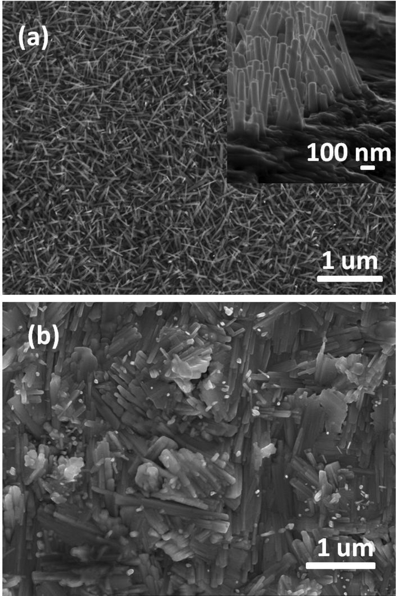 | ||
| Fig. 1 SEM images of a WOx layer grown on a W substrate at Tsub = 700 °C in the presence of pO2 = 10 mTorr for t = 45 min (a) with and (b) without the contribution from 193 nm ablation of the WO3 target at F = 10 J cm−2. The inset in (a) shows a section (tilt view) through the PLD-assisted NR array obtained after cleaving the sample. | ||
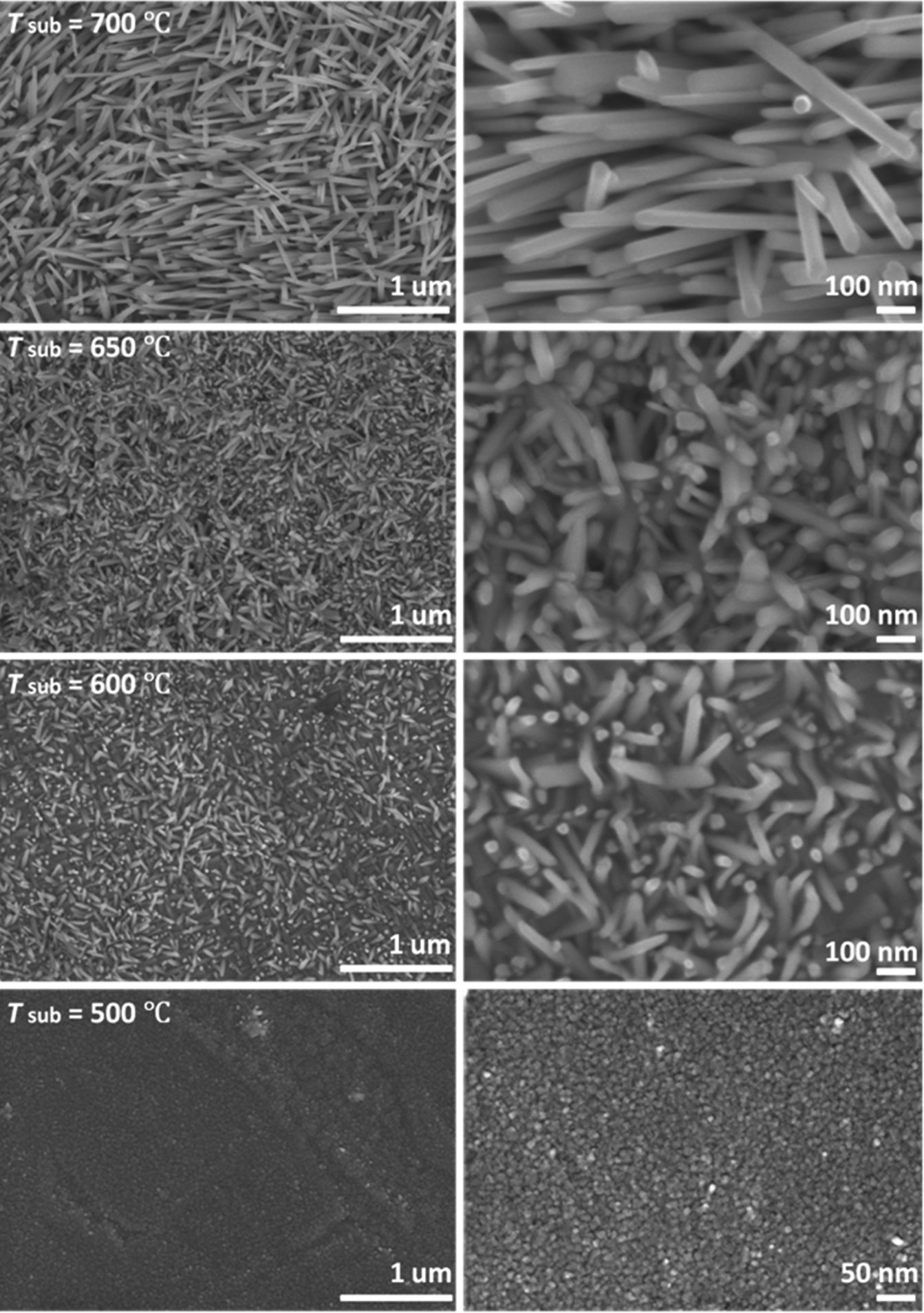 | ||
| Fig. 2 Low and high resolution SEM images (left and right hand columns, respectively) illustrating the Tsub dependence of the morphology of the WOx layer formed on a W substrate by 193 nm ablation of the WO3 target at F = 10 J cm−2 in pO2 = 10 mTorr for t = 45 min. | ||
Fig. 3(a) shows XRD spectra of the with-PLD WOx-on-W sample shown in Fig. 1(a) and a sample from the polycrystalline target (scraped onto a Si support). The three peaks at 2θ ∼ 23–24.5° in the spectrum of the target material confirms its predominantly monoclinic nature (JCPDS no. 43-1035), whereas the XRD spectrum of the with-PLD (and the PLD-free) samples are dominated by the (200) and (400) reflections of cubic-WO3 (JCPDS no. 46-1096, labelled according to a 7.6 Å unit cell) and the W substrate itself. The dominance of these reflections implies preferential (100) alignment, that we assume to be directed by the oxidizing substrate. Fig. 3(b) and (c) illustrate the effects of, respectively, increasing Tsub (at constant pO2 = 10 mTorr) and increasing pO2 (at constant Tsub = 700 °C) as evidenced by the relative intensities of the (200) reflections of WO3 and W (at 2θ = 23.6 and 58.3°, respectively) – with the largest ratio in each plot arbitrarily scaled to 1.0. Clearly, increasing Tsub and pO2 both have the effect of increasing the relative intensity of the WO3 reflection, but the relative intensities of the various WO3 reflections in any one XRD spectrum show little sensitivity to these changes, and the main factor behind these trends is likely to be the amount of deposited material. By way of comparison, the corresponding ratio for the case of a PLD-free film grown for the same duration at Tsub = 700 °C and pO2 = 10 mTorr is 0.22.
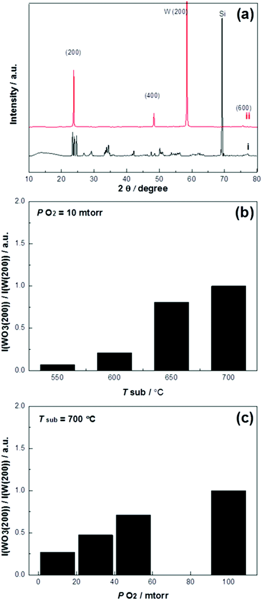 | ||
| Fig. 3 (a) XRD spectra of (i) material scraped from the WO3 target onto a Si substrate (that confirms the (predominantly) monoclinic structure of the target material) and (ii) the WOx layer formed on a W substrate maintained at Tsub = 700 °C by 193 nm ablation of the WO3 target at F = 10 J cm−2 in the presence of pO2 = 10 mTorr for t = 45 min (the dominant peaks in which are attributable to (100) aligned cubic-WO3 (as well as peaks from the underlying W substrate)). The lower panels show the way the relative intensities of the (200) reflections of WO3 and W in XRD spectra of PLD-grown samples vary with (b) Tsub (at pO2 = 10 mTorr) and (c) pO2 (at Tsub = 700 °C). The ratios in (b) and (c) have been scaled such that the largest ratio in each case is 1.0. | ||
TEM analysis reveals further subtleties. The low resolution TEM image of material broken from the with-PLD sample (Fig. 4(a)) provides an estimate of the NR lengths (which reach ![[small script l]](https://www.rsc.org/images/entities/i_char_e146.gif) ∼ 700 nm) and diameters. The latter vary among the different NRs, spanning the range 50–80 nm, but remain fairly constant along the length of any one NR. Fig. 4(b) and (c) show, respectively, a HRTEM image from near the tip of a single NR and the SAED pattern recorded from this NR. The latter is consistent with a (001) orientation of cubic-WO3 and a [100] growth direction – in accord with the XRD data (Fig. 3(c)) – while the obvious streaking in the (020) reflection implies the presence of numerous stacking faults in this direction. The closely spaced diffraction spots apparent in the diffraction streaks also suggest a long range ordering of the stacking faults. These observations are consistent with the HRTEM image (Fig. 4(b)), which shows single crystal regions with clearly defined fringe spacings of d ∼ 0.38 nm (characteristic of cubic-WO3) separated by obvious stacking faults where the registry of the planes slips by, for example, half a fringe spacing. Such herring-bone-like patterns, which imply the presence of multiple superimposed crystallographic domains bounded by stacking faults, or crystallographic shears, have also been reported previously16,30,31 and are a characteristic signature of sub-stoichiometric tungsten trioxide (WO3−δ).
∼ 700 nm) and diameters. The latter vary among the different NRs, spanning the range 50–80 nm, but remain fairly constant along the length of any one NR. Fig. 4(b) and (c) show, respectively, a HRTEM image from near the tip of a single NR and the SAED pattern recorded from this NR. The latter is consistent with a (001) orientation of cubic-WO3 and a [100] growth direction – in accord with the XRD data (Fig. 3(c)) – while the obvious streaking in the (020) reflection implies the presence of numerous stacking faults in this direction. The closely spaced diffraction spots apparent in the diffraction streaks also suggest a long range ordering of the stacking faults. These observations are consistent with the HRTEM image (Fig. 4(b)), which shows single crystal regions with clearly defined fringe spacings of d ∼ 0.38 nm (characteristic of cubic-WO3) separated by obvious stacking faults where the registry of the planes slips by, for example, half a fringe spacing. Such herring-bone-like patterns, which imply the presence of multiple superimposed crystallographic domains bounded by stacking faults, or crystallographic shears, have also been reported previously16,30,31 and are a characteristic signature of sub-stoichiometric tungsten trioxide (WO3−δ).
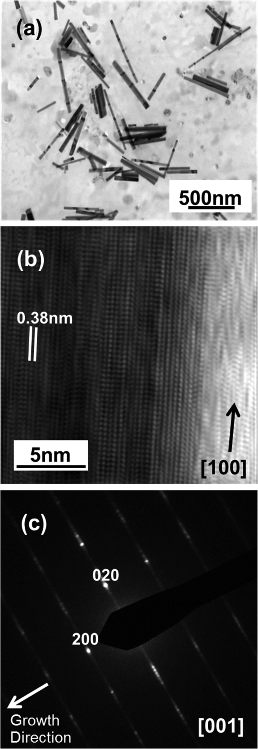 | ||
| Fig. 4 (a) Low resolution TEM image of material broken from the WOx layer grown on a W substrate at Tsub = 700 °C in the presence of pO2 = 10 mTorr for t = 45 min with the contribution from 193 nm ablation of the WO3 target at F = 10 J cm−2. (b) HRTEM image of the tip of a single NR, showing the d = 0.38 nm fringe spacing and an obvious stacking fault. (c) SAED pattern taken from this NR sample, indexed as cubic-WO3. | ||
3.2. Growth on Ta substrates
Similar process conditions enable growth of dense arrays of WOx NRs on Ta substrates. Optimal conditions were established as Tsub ∼ 700 °C and pO2 = 50 mTorr, as illustrated by the SEM image of a with-PLD sample grown for t = 45 min shown in Fig. 5(c). As with a W substrate, the form of the deposited material is very sensitive to the choice of Tsub; deposition for the same t and with the same pO2 but lower Tsub yielded either sparse clumps of NRs or none at all (Fig. 5(a) and (b)). Deposition at Tsub ∼ 700 °C but with lower pO2 (e.g. 10 mTorr) again yielded dense NR arrays, but with smaller aspect ratio (as illustrated in Fig. 5(d)). XRD analysis reveals that the dominant phase evolves with Tsub. Fig. 6 shows XRD data from several samples grown at different Tsub but constant pO2 = 50 mTorr; XRD spectra of samples grown in pO2 = 10 mTorr show all the same trends. All peaks in the XRD spectra of samples prepared at Tsub < 550 °C are attributable to the Ta foil substrate – consistent with the amorphous appearance of the WOx layer in the corresponding SEM image (Fig. 5(a)). Additional reflections are observed in the XRD spectra of samples deposited at Tsub ≥ 550 °C, all of which are seen (by SEM) to support NRs. None of the additional peaks can be assigned to cubic-WO3 (Fig. 3), but most align well with documented low-order reflections from the hexagonal phase of WO3 (JCPDS no. 33-1387).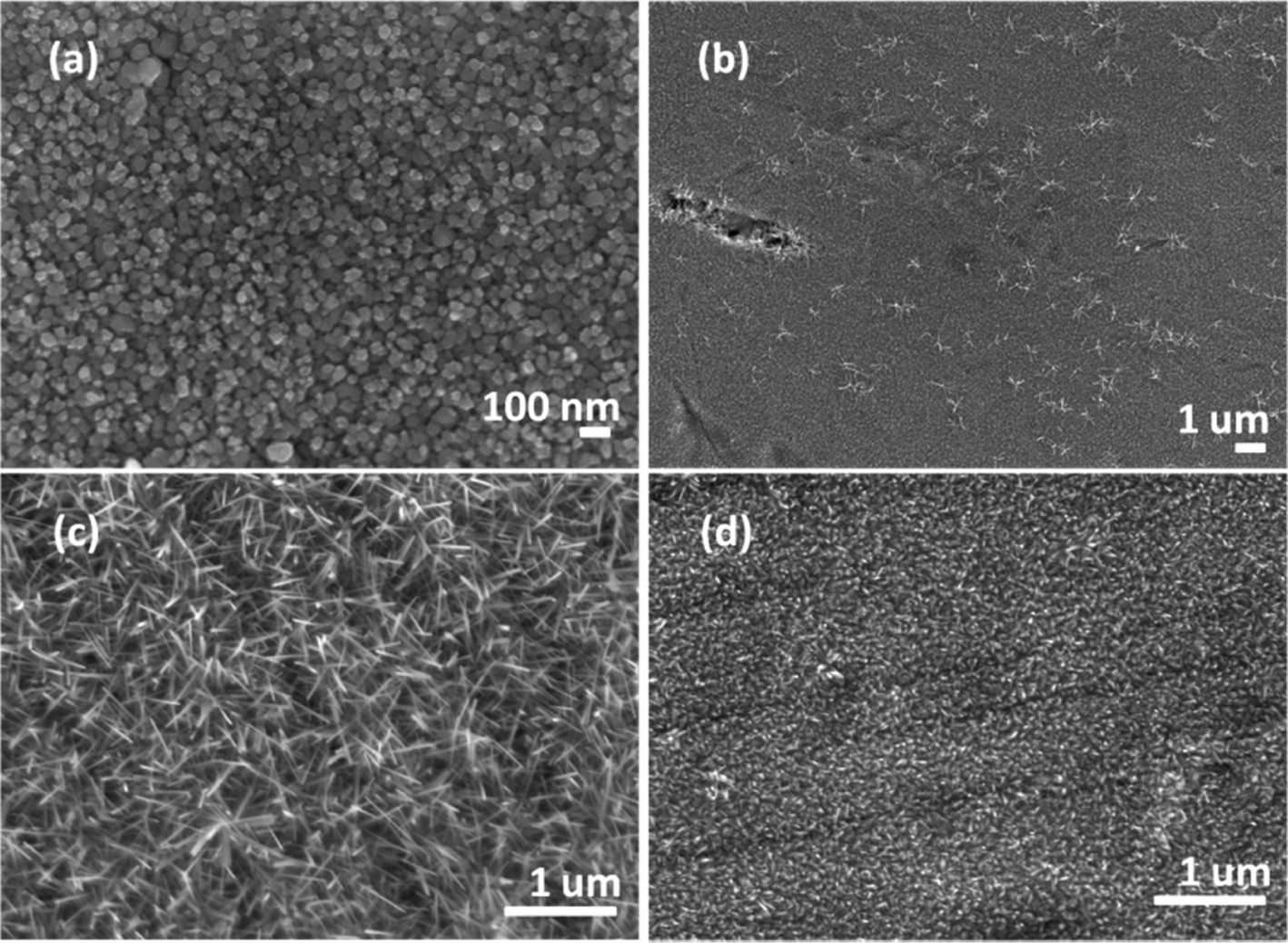 | ||
| Fig. 5 SEM images of WOx layers grown by 193 nm ablation of the WO3 target for t = 45 min on Ta substrates under the following conditions of Tsub and pO2: (a) 450 °C, 50 mTorr; (b) 550 °C, 50 mTorr; (c) 700 °C, 50 mTorr; (d) 700 °C, 10 mTorr. | ||
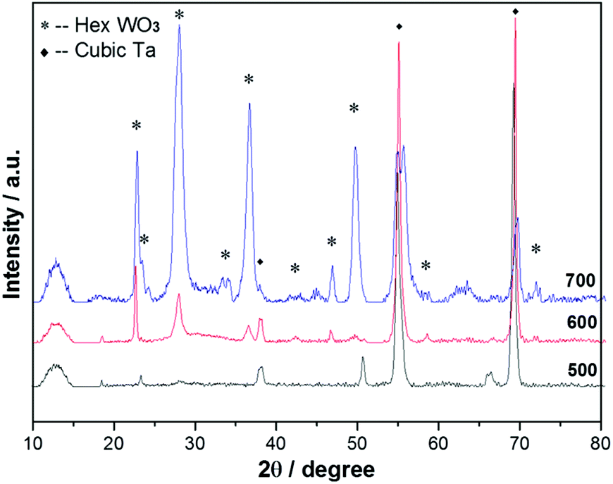 | ||
| Fig. 6 XRD spectra of WOx layers grown on Ta by 193 nm ablation of the WO3 target for t = 45 min in pO2 = 50 mTorr at Tsub = 500, 600 and 700 °C. Diffraction peaks attributable to hexagonal-WO3 are evident in spectra of samples grown at Tsub ≥ 550 °C as indicated by the symbols above the upper most trace. | ||
Once again, however, TEM analysis reveals further subtleties. Low-resolution TEM images of NRs grown by PLD on Ta for t = 45 min at Tsub = 700 °C and pO2 = 50 mTorr (Fig. 7(a)) show clear similarities with those of the NRs grown on W (Fig. 4(a)), but HRTEM and SAED investigations imply the presence of more than one phase. The HRTEM images of all of the NRs subjected to detailed analysis show the d ∼ 0.38 nm lattice spacing associated with cubic-WO3 and very obvious stacking faults (see e.g.Fig. 7(b)); again, the associated SAED images show some streaking in the (020) reflection (Fig. 7(c)). Electron diffraction patterns taken from larger areas (e.g. from a clump of NRs, Fig. 7(d)) show a more complex pattern of diffraction rings, the separations between which imply a dominant contribution from hexagonal WO3![[thin space (1/6-em)]](https://www.rsc.org/images/entities/char_2009.gif) 32 – as implied by the XRD data (which is also taken from areas much larger than that of a single NR). Thus we conclude that PLD on Ta substrates at Tsub ≥ 550 °C yields both cubic and hexagonal WO3−x. XRD analysis suggests a predominance of hexagonal phase material in the total deposit, but the HRTEM studies indicated that many of the better formed NRs have a cubic crystal structure.
32 – as implied by the XRD data (which is also taken from areas much larger than that of a single NR). Thus we conclude that PLD on Ta substrates at Tsub ≥ 550 °C yields both cubic and hexagonal WO3−x. XRD analysis suggests a predominance of hexagonal phase material in the total deposit, but the HRTEM studies indicated that many of the better formed NRs have a cubic crystal structure.
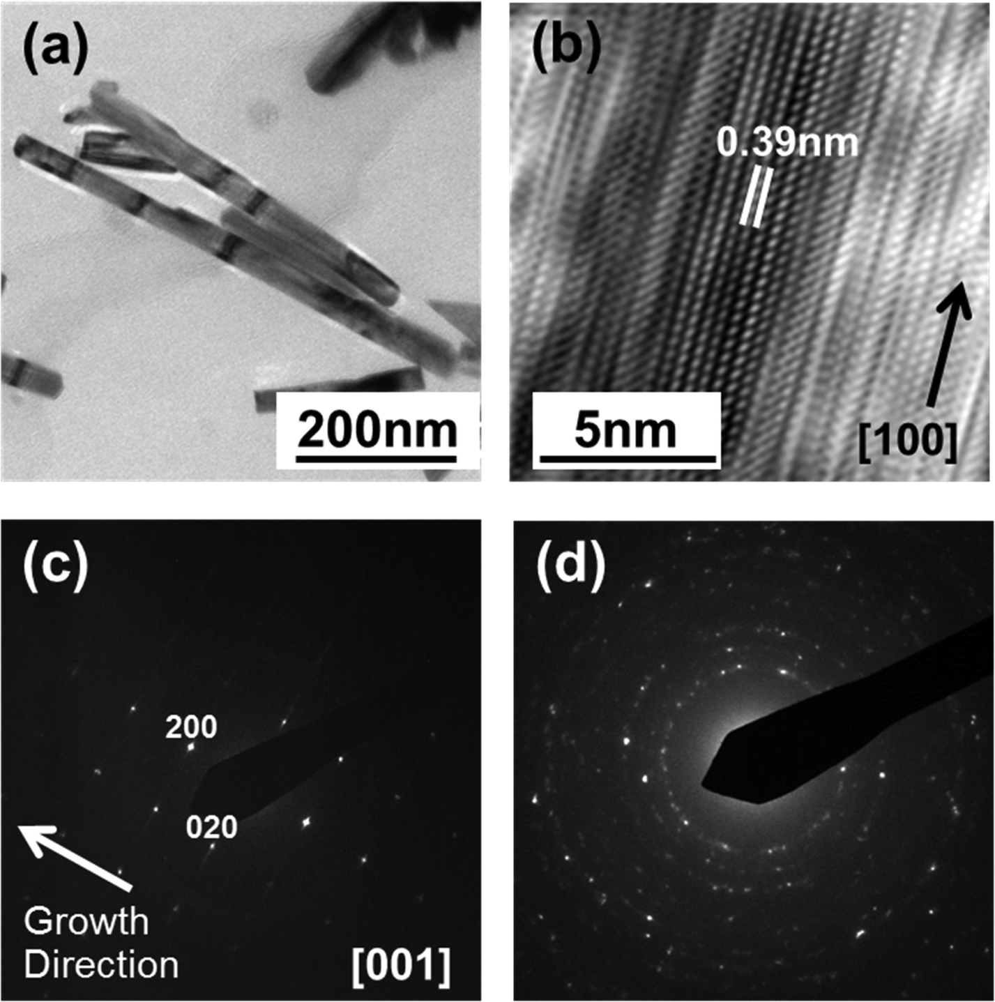 | ||
| Fig. 7 (a) Low resolution TEM image of NRs broken from the WOx layer grown on a Ta substrate at Tsub = 700 °C by 193 nm ablation of the WO3 target in the presence of pO2 = 50 mTorr for t = 45 min. (b) HRTEM and (c) SAED images taken from a single NR, illustrating the cubic-WO3 microstructure. (d) SAED image taken from a clump of NRs; the ring separations fit well with that expected for hexagonal WO3. | ||
3.3. Growth on Cu substrates
Tungsten oxide NRs were also successfully grown on Cu substrates but, as Fig. 8 and 9 show, these have a very different morphology. Again, we identify an optimum process window as illustrated by the SEM images shown in Fig. 8, all of which samples were deposited under pO2 = 10 mTorr for t = 45 min. The morphology of the deposited material is very sensitive to Tsub, and ranges from a ‘cobbled’ coating at Tsub = 400 °C, through an array of fine NRs at Tsub = 500 °C, to a film composed of larger crystallites at 600 °C. The cross-section image (Fig. 8(b), inset) shows that the NRs on Cu are less dense than those on Ta or W substrates, and sit on a dense underlying thatch of deposited material. The very different appearance of these NRs (cf. those grown on W or Ta substrates) is shown more clearly by the image of an as-grown tangle of NRs (Fig. 9(a)) and of a ‘single’ NR in Fig. 9(b). The NR has a ‘tree-like’ appearance, with first- (and in some cases second-) generation ‘daughter’ NRs emerging perpendicular to the shaft of the parent NR. These dendritic structures are somewhat reminiscent of those reported in prior studies where W foil (covered by a SiO2 plate) was heated in Ar at 1600 °C,33 where W powder was heated in oxygen to 1400–1450 °C,6,34 and where PLD-grown WOx films were subsequently thermally annealed in vacuum and then in air.35 The daughter NRs in the present work appear to grow from an edge of the parent NR, as shown in the inset to Fig. 9(b), rather than the face (as suggested by some of these prior studies). Compared with the WOx NRs grown on W and Ta, the NRs grown on Cu are ‘macroscopic’: many μm in length, generally much thicker at the base, and clearly tapering in the growth direction; many terminate with a narrow tip (Fig. 9(c)).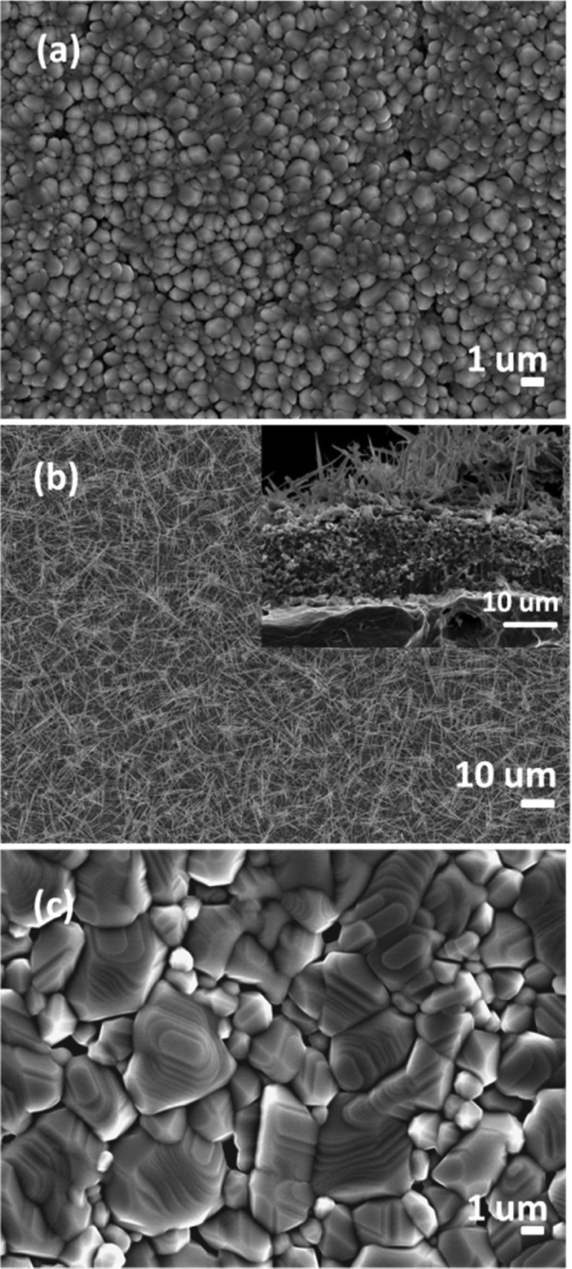 | ||
| Fig. 8 SEM images of WOx layers grown by 193 nm ablation of the WO3 target for t = 45 min on a Cu substrate in the presence of pO2 = 10 mTorr at Tsub = (a) 400 °C; (b) 500 °C; and (c) 600 °C. The cross-section image of the deposit grown at Tsub = 500 °C (inset in panel (b)) shows a tangle of poorly aligned NRs emerging from a dense thatch of underlying material. | ||
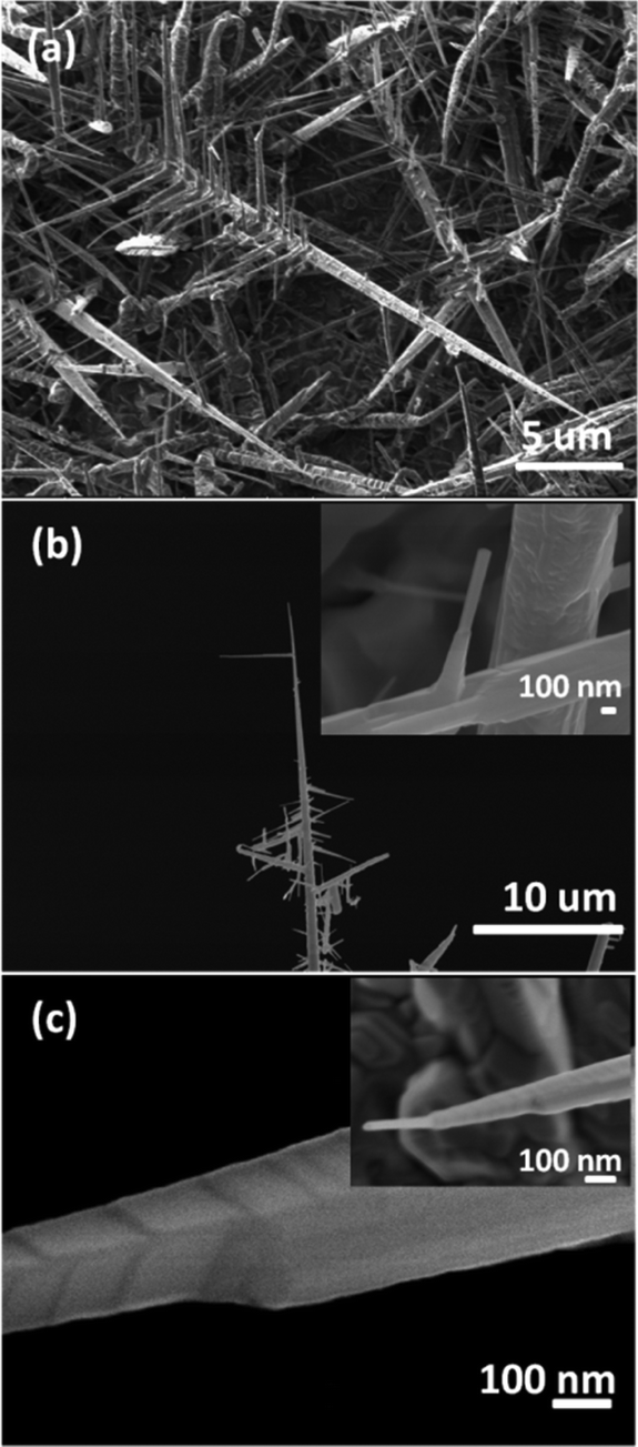 | ||
| Fig. 9 Progressively higher resolution SEM images of WOx NRs grown on a Cu substrate in the presence of pO2 = 10 mTorr by 193 nm ablation of the WO3 target for t = 45 min at Tsub = 500 °C: (a) an as-grown tangle of tree-like NRs; (b) a ‘single’ NR demonstrating the emergence of first (and in some cases second) generation daughter NRs at right angles to and from the edge of (see inset) the shaft of the parent NR; (c) detail of the end of a single NR shaft, illustrating obvious faceting and tapered morphology in the growth direction. | ||
As Fig. 10 shows, the as-grown material exhibits a simple XRD spectrum with clear peaks at 2θ = 15.2, 18.1, 31.6 and 36.2° that are not attributable to the Cu substrate. We have not succeeded in matching these with any documented WOx structure, though we note that peaks at ∼18° and ∼37° have previously been identified as (111) and (222) reflections of orthorhombic WO3.36 As noted above, the XRD measurements inherently sample a large (∼1 cm2) area, so the relative contributions made by the dendritic NRs and the underlying thatch to the total XRD spectrum is unclear. The SAED patterns shown in Fig. 11, in contrast, are taken from the tapered tip of a single NR and are clearly consistent with a cubic structure with lattice parameter a = 0.38 nm. Panel (a) in Fig. 11 shows a (001) diffraction pattern (i.e. with an [001] zone axis parallel to the electron beam direction) with the NR growth direction [100] indicated by the arrow, while Fig. 11(b) shows the corresponding SAED pattern taken along the [101] axis (obtained by tilting the NR by 45° about [010], such that the (040) reflection is common to both patterns). The appearance of the (020) reflection in the [101] pattern but not in the [001] pattern is consistent with {200} reflections being kinematically forbidden, with excitation depending on double diffraction routes which are present in the [101], but not in the [001], orientation.
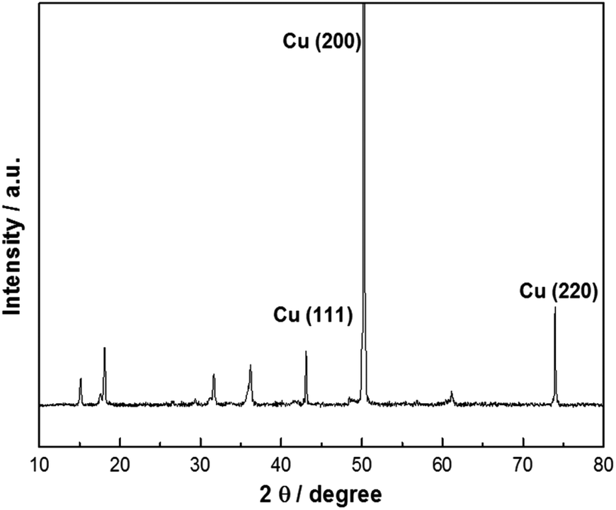 | ||
| Fig. 10 XRD spectrum of the WOx layer grown on Cu by 193 nm ablation of the WO3 target for t = 45 min in pO2 = 10 mTorr and at Tsub = 500 °C. Peaks attributable to the Cu substrate are assigned, leaving four unassigned peaks that we attribute to WOx. | ||
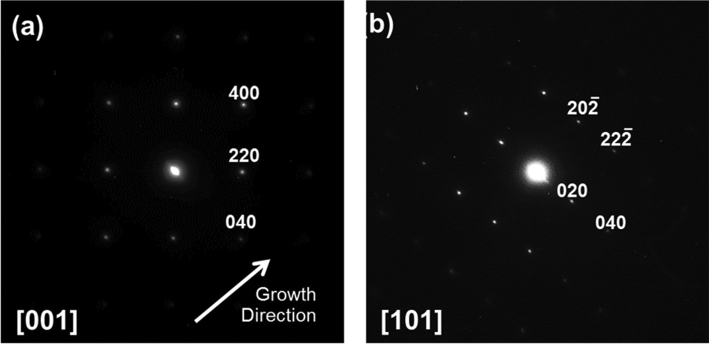 | ||
| Fig. 11 SAED patterns recorded from near the tip of a single WOx NR grown on Cu by 193 nm ablation of the WO3 target for t = 45 min in pO2 = 10 mTorr and at Tsub = 500 °C. Image (a) shows a (001) diffraction pattern (i.e. with an [001] zone axis parallel to the electron beam direction), with the arrow indicating the NR growth direction [100], while (b) shows the corresponding pattern taken along the [101] axis (obtained by tilting the NR by 45° about [010]). The (040) reflection is thus common to both patterns. | ||
Fig. 12(a) and (b) show an HRTEM image and an SAED pattern taken from the ends of other tapered crystals like that shown in the inset to Fig. 8(c). The SAED pattern is clearly different from those in Fig. 11 but if, for simplicity, we take the NR axis to be a [100] axis of the tip crystal, we can identify the main reflections nominally as {400}-type, with spacings of 0.19 nm that match well with the spacing of the {400} reflections identified in Fig. 11. The pair of spots arrowed in Fig. 12(b) can be reproduced by a model of the type shown in Fig. 12(d), based on WnO3n−1 structures, where crystallographic shear faults separate n planes of corner sharing WO6 octahedra.30,31 The structure and simulated diffraction pattern shown in Fig. 12(d) and (c) correspond to n = 4, i.e. W4O11. Experimentally, there is prominent streaking perpendicular to the NR axis, rather than the regular superlattice in Fig. 12(c), suggesting that n and the corresponding stoichiometry vary on a fine scale. These features are consistent with the lattice image in Fig. 12(a) (taken from a different crystal), which shows small regions that display a regular and approximately square cross-grating pattern, with 0.38 nm spacing, as well as an irregular structure perpendicular to the NR axis.
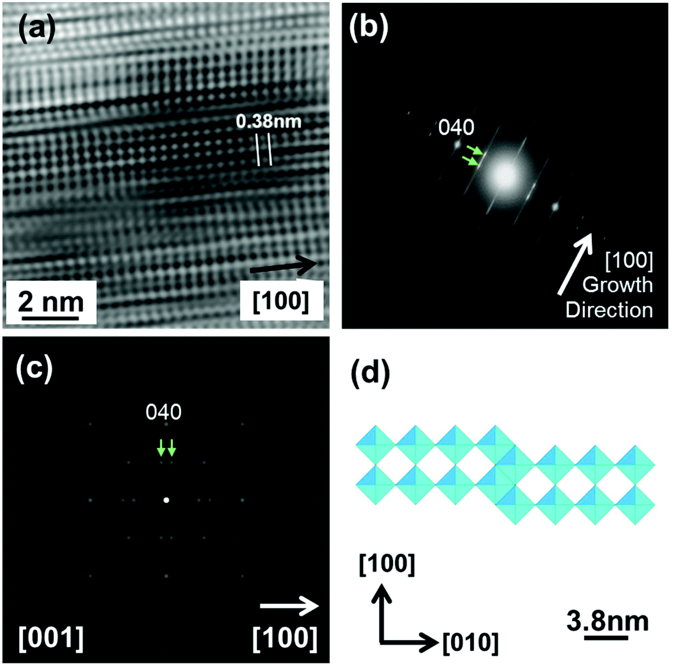 | ||
| Fig. 12 (a) HRTEM and (b) SAED images recorded near the tip of single WOx NRs grown on Cu by 193 nm ablation of the WO3 target for t = 45 min in pO2 = 10 mTorr and at Tsub = 500 °C, (c) simulated diffraction pattern for the model structure shown in (d), a unit cell for a W4O11 structure where crystallographic shear faults separate 4 planes of corner sharing WO6 octahedra. The two arrowed reflections in (c) can be compared with those arrowed in (b). | ||
Selected WOx samples grown on Cu were also investigated by XPS though, as with XRD, we caution that XPS analysis must return a superposition of compositional information for both the NRs and the underlying thatch. Expanded views of the W 4f and O 1s binding energy regions are shown in Fig. 13. The former can be decomposed (Fig. 13(a)) into a doublet of doublets, attributable to the 4f7/2 and 4f5/2 peaks of both the W6+ and W5+ oxidation states.37,38 The presence of two oxidation states provides further indication that the material is sub-stoichiometric WO3−δ, as does the obvious tailing of the O 1s peak to higher binding energies (Fig. 13(b)). The illustrative decomposition shown in Fig. 13(b), along with an assumed assignment of the 530.2 and 531.4 eV peaks to O atoms in, respectively, stoichiometric WO3 and sub-stoichiometric WO3−δ,39,40 implies a mean composition with δ ≈ 0.2.
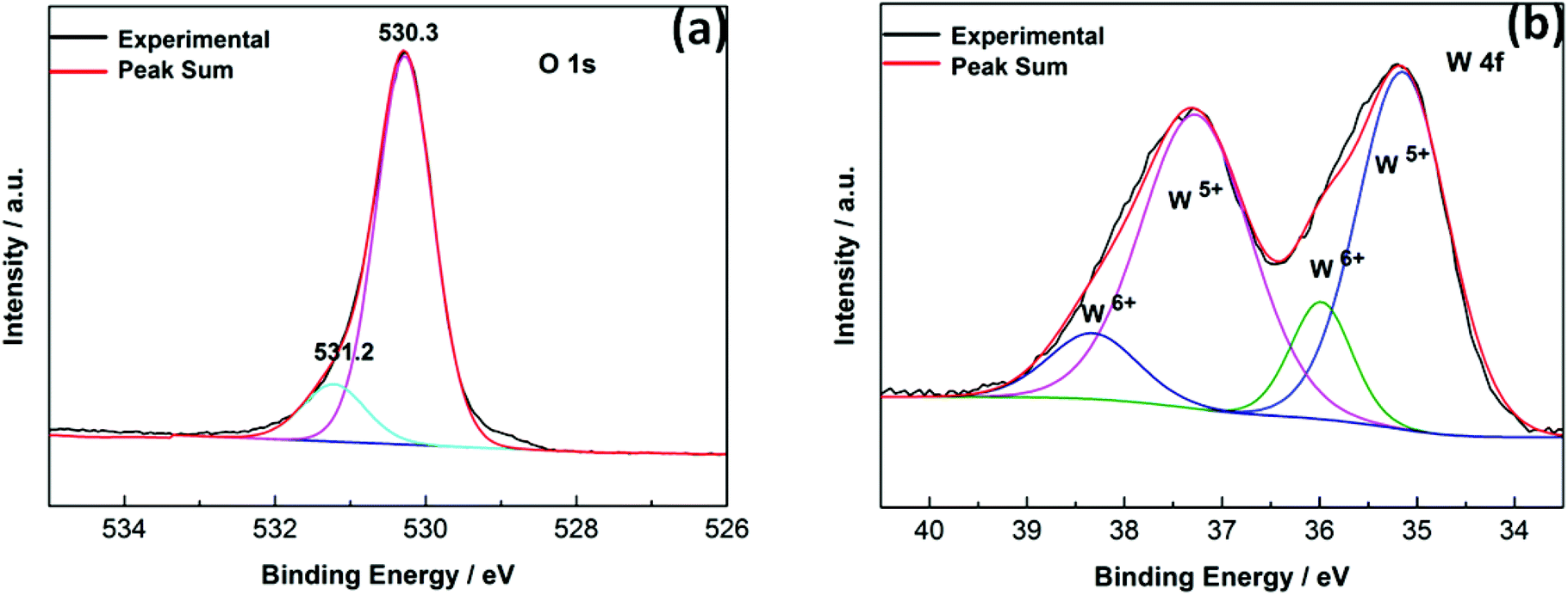 | ||
| Fig. 13 Detailed views of the O 1s and W 4f peaks in the X-ray photoelectron spectrum of the WOx-on-Cu sample grown by 193 nm ablation of the WO3 target for t = 45 min in pO2 = 10 mTorr and at Tsub = 500 °C, decomposed as described in the text. | ||
3.4. Raman spectroscopy of as-grown WOx samples
Features in Raman spectra of WOx samples are traditionally viewed in three separate wavenumber regions, depending on their physical origin. Peaks at wavenumbers <200 cm−1 are associated with lattice modes (tilting or translations of the WO6 octahedra); features in the 200–400 cm−1 region can be assigned to W–O–W stretch and/or O–W–O bending modes; while O–W–O stretching modes typically fall in the 600–900 cm−1 range.41,42 The Raman spectrum of the polycrystalline target recorded under 632.8 nm illumination (curve (a) in Fig. 14) shows clear features at 273, 324, 716 and 807 cm−1, all of which are characteristic of monoclinic WO3. However, the additional weak features at 182 and 569 cm−1 (which match no documented Raman peaks of monoclinic WO3) hint at some contribution from other phases. Both of these conclusions accord well with the preceding XRD analysis.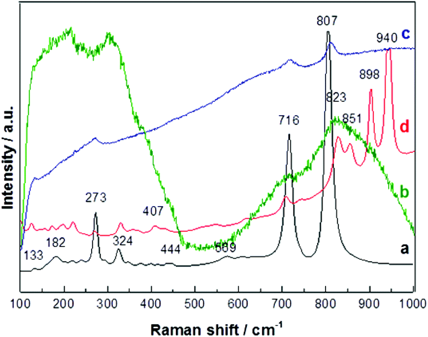 | ||
| Fig. 14 Raman spectra (632.8 nm excitation) of (a) the polycrystalline WO3 target and of the NR-rich WOx deposits grown on (b) W, (c) Ta and (d) Cu substrates by 193 nm ablation of the WO3 target for t = 45 min using pO2 and Tsub values appropriate for optimal NR growth in each case. Wavenumbers of many of the more prominent peaks are superimposed above the relevant trace. | ||
Curves (b), (c) and (d) in Fig. 14 show Raman spectra of NR-rich deposits grown on W, Ta and Cu substrates, respectively. (b) and (c) both show broad features centered around 273, 716 and 807 cm−1, but the breadth of these features (which must involve scattering from both the NRs and the underlying thatch) limits the utility of Raman spectroscopy as a compositional diagnostic in these cases. Curve (d) shows much more structure, with the peaks at high wavenumber particularly notable. Based on the previous literature,41 it is tempting to assign the 823 and 851 cm−1 features to O–W–O stretching modes, with the shift to higher wavenumber reflecting some shortening (stiffening) of the relevant bonds between the edge sharing octahedra. The 940 cm−1 feature is associated with terminal W![[double bond, length as m-dash]](https://www.rsc.org/images/entities/char_e001.gif) O bonds. This feature is commonly observed in the Raman spectra of nanocrystalline WOx samples; indeed, arguments have appeared43 suggesting that its intensity relative to that of the O–W–O stretch bands can be used as a measure of surface-to-volume ratio or cluster size. The present data may lend some support to this argument given that these features are particularly evident in the Raman spectrum of material deposited on a Cu substrate which, as Fig. 9 showed, is rich in the dendritic NR structures.
O bonds. This feature is commonly observed in the Raman spectra of nanocrystalline WOx samples; indeed, arguments have appeared43 suggesting that its intensity relative to that of the O–W–O stretch bands can be used as a measure of surface-to-volume ratio or cluster size. The present data may lend some support to this argument given that these features are particularly evident in the Raman spectrum of material deposited on a Cu substrate which, as Fig. 9 showed, is rich in the dendritic NR structures.
3.5. Field emission measurements on as-grown WOx samples
Field emission (FE) measurements were performed at room temperature in a test chamber (base pressure ∼5 × 10⁻⁷ Torr) that has been described previously.44 The WOx samples acted as the cathode, the anode comprised a phosphor screen coated with a 10 nm layer of gold, and the cathode–anode separation was maintained at d = 420 μm using a silica spacer and an aperture that defines an effective sampling area A = 0.076 cm2. The voltage, V, applied to each sample was ramped up and down once and the emission current, I, measured to obtain an initial I–V curve, and the sample was then ‘conditioned’ by cycling a further 5 times to encourage the release of any impurities.The I–V data shown in Fig. 15(a) for NR-rich WOx samples grown on W, Ta and Cu substrates are the average values returned from the next 10 up-down cycles. As is customary, we plot the emission current density, J (= I/A, in mA cm−2) vs. electric field, E (= V/d, in V μm−1). Only the sample grown on Cu exhibits encouraging FE properties, with a turn on field (which we choose to define as the field yielding an emission current density of 10 μA cm−2) of ∼5 V μm−1 –comparable to that reported for nanostructured WOx samples in other recent studies.45–47 The associated Fowler–Nordheim plot48 (i.e. plot of ln(J/E2) vs. 1/E, which is shown as an inset to Fig. 15(a)), shows two linear regions (with a steeper slope in the high field region) pivoting at 1/E ∼ 0.17 V−1 μm. The form of this plot is reminiscent of that reported in a previous study of FE from WOx nanowires grown on electrochemically sharpened tungsten tips49 and, as in that case, can plausibly be attributed to the disperse spread of NR lengths, diameters and orientations supported by the sample.
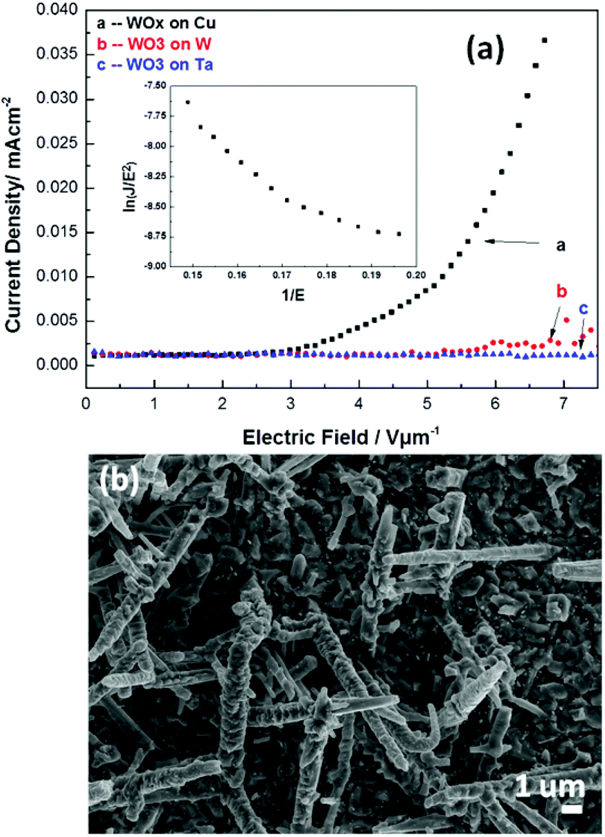 | ||
| Fig. 15 (a) Field emission current vs. applied field plot for a NR-rich WOx deposit on a Cu substrate grown under conditions as for the material shown in Fig. 9(a), along with the corresponding Fowler–Nordheim plot (inset). (b) SEM image of such a sample after application of a 12 V μm−1 field, illustrating the destruction of the finer nanostructures caused by over-driving the emission. | ||
The stability of the FE from a NR-rich WOx on Cu sample was examined at a fixed (6.1 V μm−1) field by logging the current every 1.3 s. Apart from some transient spikes, the emission remained stable at ∼15 μA (fluctuating by <10%) over the duration of the measurement (35 hours). SEM analysis of this sample post FE testing showed no discernible change to the sample morphology, but ramping the field up to 12 V μm−1 resulted in an immediate and dramatic drop in emission intensity. The SEM image of this over-driven sample (Fig. 15(b)) reveals large structural changes; the finer tips and branches have been destroyed, leaving just the parent NR shafts with a much rougher surface morphology.
4. Conclusions
The present study reports the growth of tungsten oxide NRs by 193 nm pulsed laser deposition in a low background pressure of oxygen, and subsequent characterisation of the as-grown material by SEM and HRTEM, SAED, XRD, Raman and XPS. The morphology of the deposited material is found to be sensitively dependent upon the choice of deposition conditions, including the substrate material itself. HRTEM analysis shows that NRs formed on W, Ta and Cu substrates each grow along the [100] direction and display obvious stacking faults running along this direction. Such faults also reveal themselves by streaking in the SAED pattern, perpendicular to the growth axis – implying that the NR composition is sub-stoichiometric WO3−δ in each case. The NR morphologies are very different, however. NRs formed on W or Ta substrates are short (100 s of nm in length) and display uniform cross-sections, while those grown on the Cu substrate are typically longer, thicker, tapered, and display a branched, dendritic microstructure. Only these latter NRs are found to give significant field emission.Acknowledgements
The authors are grateful to EPSRC, the China Scholarship Council, the National Science Foundation of China (grant no. 61176005 and 61006001) and the Higher Education Commission of Pakistan for financial support, and to J.N. Hart, J.A. Jones, Dong Liu, M.Z. Othman, K.N. Rosser, T.B. Scott, J.A. Smith, B.S. Truscott and Y.S. Zou for their many and varied contributions to the described work.References
- H. D. Zheng, J. Z. Ou, M. S. Strano, R. B. Kaner, A. Mitchell and K. Kalantar-Zadeh, Adv. Funct. Mater., 2011, 21, 2175 CrossRef CAS , and references therein.
- C. G. Granqvist, Handbook of Inorganic Electrochromic Materials, Elsevier, New York, 1995 Search PubMed.
- G. A. Niklasson and C. G. Granqvist, J. Mater. Chem., 2007, 17, 127 RSC.
- See, for example, Z. G. Zhao and M. Miyauchi, Angew. Chem., Int. Ed., 2008, 47, 7051 CrossRef CAS PubMed.
- See, for example, X. Liu, F. Wang and Q. Wang, Phys. Chem. Chem. Phys., 2012, 14, 7894 RSC.
- A. Ponzoni, E. Comini, G. Sberveglieri, J. Zhou, S. Z. Deng, N. S. Xu, Y. Ding and Z. L. Wang, Appl. Phys. Lett., 2006, 88, 203101 CrossRef PubMed.
- R. S. Devan, R. A. Patil, J. H. Lin and Y. R. Ma, Adv. Funct. Mater., 2012, 22, 3326 CrossRef CAS , and references therein.
- See, for example, H. Zheng, Y. Tachibana and K. Kalantar-Zadeh, Langmuir, 2010, 26, 19148 CrossRef CAS PubMed.
- J. G. Allpress, R. J. D. Tilley and M. J. Sienko, J. Solid State Chem., 1971, 3, 440 CrossRef CAS.
- Z. J. Gu, T. Y. Zhai, B. F. Gao, X. H. Zheng, Y. B. Wang, H. B. Fu, Y. Ma and J. N. Yao, J. Phys. Chem. B, 2006, 110, 23829 CrossRef CAS PubMed.
- J. M. Wang, E. Khoo, P. S. Lee and J. Ma, J. Phys. Chem. C, 2008, 112, 14306 CAS.
- K. Kalantar-Zadeh, A. Vijayaraghavan, M.-H. Ham, H. D. Zheng, M. Breedon and M. S. Strano, Chem. Mater., 2010, 22, 5660 CrossRef CAS.
- H. W. Zhang, G. T. Duan, Y. Li, X. X. Xu, Z. F. Dai and W. P. Cai, Cryst. Growth Des., 2012, 12, 2646 CAS.
- H. W. Zhang, Y. Li, G. T. Duan, G. Q. Liu and W. P. Cai, CrystEngComm, 2014, 16, 2491 RSC.
- J. Thangala, S. Vaddiraju, R. Bogale, R. Thurman, T. Powers, B. Deb and M. K. Sunkara, Small, 2007, 3, 890 CrossRef CAS PubMed.
- A. M. Smith, M. G. Kast, B. A. Nail, S. Aloni and S. W. Boettcher, J. Mater. Chem. A, 2014, 2, 6121 CAS.
- F. Mitsugi, E. Hiraiwa, T. Ikegami, K. Ebihara and R. K. Thareja, Jpn. J. Appl. Phys., Part 1, 2002, 41, 5372 CrossRef CAS.
- T. Aoki, T. Matsushita, A. Suzuki, K. Tanabe and M. Okuda, J. Vac. Sci. Technol., A, 2005, 23, 1325 CAS.
- C. V. Ramana, S. Utsunomiya, R. C. Ewing, C. M. Julien and U. Becker, J. Phys. Chem. B, 2006, 110, 10430 CrossRef CAS PubMed.
- Y. Suda, H. Kawasaki, T. Ohshima and Y. Yagyuu, Thin Solid Films, 2008, 516, 4397 CrossRef CAS PubMed.
- K. J. Lethy, D. Beena, R. V. Kumar, V. P. M. Pillai, V. Ganesan and V. Sathe, Appl. Surf. Sci., 2008, 254, 2369 CrossRef CAS PubMed.
- N. Santo, M. Filipescu, P. M. Ossi and M. Dinescu, Appl. Phys. A, 2010, 101, 325 CrossRef CAS.
- Y. S. Zou, Y. C. Zhang, D. Lou, H. P. Wang, L. Gu, Y. H. Dong, K. Dou, X. F. Song and H. B. Zeng, J. Alloys Compd., 2014, 583, 465 CrossRef CAS PubMed.
- M. H. Yaacob, J. Z. Ou, W. Wlodarski, C. S. Kim, J. Y. Lee, Y. H. Kim, C. M. Oh, K. P. Dhakal, J. Y. Kim and J. H. Kang, J. Korean Phys. Soc., 2012, 60, 393 CrossRef CAS.
- M. Z. Ahmad, J. Kang, A. S. Zoolfakar, A. Z. Sadek and W. Wlodarski, J. Nanosci. Nanotechnol., 2013, 13, 8315 CrossRef CAS PubMed.
- Y. Sun, G. M. Fuge and M. N. R. Ashfold, Chem. Phys. Lett., 2004, 396, 21 CrossRef CAS PubMed.
- G. M. Fuge, T. M. S. Holmes and M. N. R. Ashfold, Chem. Phys. Lett., 2009, 479, 125 CrossRef CAS PubMed.
- T. Tokunaga, T. Kawamoto, K. Tanaka, N. Nakamura, Y. Hayashi, K. Sasaki, K. Kuroda and T. Yamamoto, Nanoscale Res. Lett., 2012, 7, 85 CrossRef PubMed.
- S. G. Jeon and J. J. Yong, J. Mater. Res., 2008, 23, 132 Search PubMed.
- T. Miyano, M. Iwanishi, C. Kaito and M. Shiojiri, Jpn. J. Appl. Phys., 1983, 22, 863 CrossRef CAS.
- J. Sloan, J. L. Hutchinson, R. Tenne, Y. Feldman, T. Tsirlina and M. Honyonfer, J. Solid State Chem., 1990, 144, 100 CrossRef.
- B. Gerand, G. Nowogrocki, J. Guenot and M. Figlarz, J. Solid State Chem., 1979, 29, 429 CrossRef CAS.
- Y. Q. Zhu, W. B. Hu, W. K. Hsu, M. Terrones, N. Grobert, J. P. Hare, H. W. Kroto, D. R. M. Walton and H. Terrones, Chem. Phys. Lett., 1999, 309, 327 CrossRef CAS.
- J. Zhou, Y. Ding, S. Z. Deng, L. Gong, N. S. Xu and Z. L. Wang, Adv. Mater., 2005, 17, 2107 CrossRef CAS.
- A. Ponzoni, V. Russo, A. Bailini, C. S. Casari, M. Ferroni, A. Li Bassi, A. Migliori, V. Morandi, L. Ortolani, G. Sberveglieri and C. E. Bottani, Sens. Actuators, B, 2011, 153, 340 CrossRef CAS PubMed.
- S. Rajagopal, D. Nataraj, D. Mangalaraj, Y. Djaoued, J. Robichaud and O. Y. Khyzhun, Nanoscale Res. Lett., 2009, 4, 1335 CrossRef CAS PubMed.
- H. Y. Wong, C. W. Ong, R. W. M. Kwok, K. W. Wong, S. P. Wong and W. Y. Cheung, Thin Solid Films, 2000, 376, 131 CrossRef CAS.
- H.-S. Shim, J. W. Kim, Y.-E. Sung and W. B. Kim, Sol. Energy Mater. Sol. Cells, 2009, 93, 2062 CrossRef CAS PubMed.
- S. Pal and C. Jacob, Appl. Surf. Sci., 2007, 253, 3317 CrossRef CAS PubMed.
- F. Y. Xie, L. Gong, X. Liu, Y. T. Tao, W. H. Zhang, S. H. Chen, H. Meng and J. Chen, J. Electron Spectrosc. Relat. Phenom., 2012, 185, 112 CrossRef CAS PubMed.
- M. F. Daniel, B. Desbat, J. C. Lassegues, B. Gerand and M. Figlarz, J. Solid State Chem., 1987, 67, 235 CrossRef CAS.
- C. Santato, M. Odziemkowski, M. Ulmann and J. Augustynski, J. Am. Chem. Soc., 2001, 123, 10639 CrossRef CAS PubMed.
- T. Kubo and Y. Nishikitani, J. Electrochem. Soc., 1998, 145, 1729 CrossRef CAS PubMed.
- Y. Zou, P. W. May, S. M. C. Vieira and N. A. Fox, J. Appl. Phys., 2012, 112, 044903 CrossRef PubMed.
- Y. B. Li, Y. Bando and D. Golberg, Adv. Mater., 2003, 15, 1294 CrossRef CAS.
- J. G. Liu, Z. J. Zhang, Y. Zhao, X. Su, S. Liu and E. G. Wang, Small, 2005, 1, 310 CrossRef CAS PubMed.
- F. Liu, T. Y. Guo, Z. Xu, H. B. Gan, L. F. Li, J. Chen, S. Z. Deng, N. S. Xu, D. Golberg and Y. Bando, J. Mater. Chem. C, 2013, 1, 3217 RSC , and references therein.
- R. H. Fowler and L. W. Nordheim, Proc. R. Soc. London, Ser. A, 1928, 119, 173 CrossRef CAS.
- R. Seelaboyina, J. Huang, J. Park, D. H. Kang and W. B. Choi, Nanotechnology, 2005, 17, 4840 CrossRef.
Footnotes |
| † Permanent address: Department of Physics, Lanzhou University, Lanzhou 730000, China. |
| ‡ Permanent address: Department of Physics, University of Sargodha, Sargodha, Pakistan. |
| This journal is © The Royal Society of Chemistry 2014 |