
 Open Access Article
 This Open Access Article is licensed under a
 Creative Commons Attribution 3.0 Unported Licence
The conquest of middle-earth: combining top-down and bottom-up nanofabrication for constructing nanoparticle based devices†
Yuri A.
Diaz Fernandez‡§
 a,
Tina A.
Gschneidtner§
a,
Carl
Wadell
b,
Louise H.
Fornander
a,
Samuel
Lara Avila
b,
Christoph
Langhammer
b,
Fredrik
Westerlund
a and
Kasper
Moth-Poulsen
*a
a,
Tina A.
Gschneidtner§
a,
Carl
Wadell
b,
Louise H.
Fornander
a,
Samuel
Lara Avila
b,
Christoph
Langhammer
b,
Fredrik
Westerlund
a and
Kasper
Moth-Poulsen
*a
aDepartment of Chemical and Biological Engineering, Chalmers University of Technology, SE-412 96 Gothenburg, Sweden. E-mail: kasper.moth-poulsen@chalmers.se
bDepartment of Applied Physics, Chalmers University of Technology, SE-412 96 Gothenburg, Sweden
First published on 21st August 2014
Abstract
The development of top-down nanofabrication techniques has opened many possibilities for the design and realization of complex devices based on single molecule phenomena such as e.g. single molecule electronic devices. These impressive achievements have been complemented by the fundamental understanding of self-assembly phenomena, leading to bottom-up strategies to obtain hybrid nanomaterials that can be used as building blocks for more complex structures. In this feature article we highlight some relevant published work as well as present new experimental results, illustrating the versatility of self-assembly methods combined with top-down fabrication techniques for solving relevant challenges in modern nanotechnology. We present recent developments on the use of hierarchical self-assembly methods to bridge the gap between sub-nanometer and micrometer length scales. By the use of non-covalent self-assembly methods, we show that we are able to control the positioning of nanoparticles on surfaces, and to address the deterministic assembly of nano-devices with potential applications in plasmonic sensing and single-molecule electronics experiments.
Introduction
One of the most exciting challenges in modern nanotechnology resides in the middle size range, bridging molecular length scales and microsized objects.1 Considerable efforts have been devoted to the development of top-down nanofabrication methods,2–9 and the impressive progress achieved by miniaturization technology in the last decades has led to advanced omnipresent microprocessors and portable devices. Yet, top-down lithography techniques are at the present level not able to fabricate systems with molecular or atomic precision.5,10–14In a parallel effort, the understanding of the physical and chemical phenomena responsible for self-organization of molecules and materials into complex hierarchical structures has launched a quest towards self-fabricating systems based on supramolecular chemistry.15–20 Experimental and theoretical contributions from different research fields have contributed to the development of self-assembled materials, formed by collective interactions of organic molecules, inorganic nanoparticles (NPs), and hybrid composites.21–25
If we consider the number of scientific publications related to top-down and bottom-up approaches in the last decades as an indicator of the development of these research fields, we can affirm that there has been a continuous growth of interest of the scientific community in these topics, catalysed by the improvement of electron microscopy techniques, scattering methods, scanning probe techniques, and other characterization tools able to provide detailed information on processes and structures with atomic resolution.26
While both extreme domains, the bottom-up and the top-down fields, have been consolidated over years of fundamental and technological research, the intermediate length-scale, the “middle” field, started to be intensively explored only recently.1,27–32 One plausible reason for this delayed debut could be the lack of experimental techniques able to address properties of single, or just-a-few, molecules, and the inability to accurately control the fate of sub-nanometric objects. One relevant challenge related to the fabrication of devices that combine single-molecule length scale objects with macroscopic objects, is the requirement of controlled positioning of NPs and molecules at pre-defined sites at surfaces.33 In the present article we highlight some efforts that our research group, together with several collaborators, have been involved in to address this issue, and we also discuss challenges and future perspectives in this field. Furthermore, we present some recent results related to the combination of self-assembly methods and top-down fabrication techniques to control positioning of NPs at surfaces.
Results & discussion
Solution based self-assembly methods
One major challenge in the development of single molecule devices is the incompatibility in length scales between molecular dimensions and macroscopic instruments. One of the approaches used to overcome this challenge is based on the self-assembly in solution of nanometric junctions between NPs and the placement of these proto-devices on micro-fabricated structures, i.e. electrodes connected to macroscopic source-drain electrodes.28,34–36 Using this approach, Bar-Joseph et al. in 2005 probed, for the first time, the transport properties across a single molecule that bridges two metal NPs.37 The interest of the research community has remained on this strategy for several years, developing sophisticated synthetic approaches to build NP aggregates of controlled size in solution,36,38–43 and to place these proto-devices onto electrodes.34–38Bjørnholm et al. developed a bottom-up approach that combines nanoparticle self-assembly and seed-growth methods to synthetize end-to-end linked gold nanorods (AuNRs).44 While several procedures for the end-to-end linking of AuNRs involve modification of the already synthetized AuNRs,45–48 Bjørnholm et al. assembled spherical NPs into small aggregates (i.e. dimers) connected by dithiol PEG linker molecules, and then used these aggregates as seeds for the growth of AuNRs. The resulting structures consisted of two 500 nm long AuNRs separated by a gap of 2 nm. Although the yields of this process were not particularly high, the possibility of combining these highly anisotropic proto-devices with micro-electrodes provides a promising path to overcome the challenges of single molecule transport measurements.28,49
Several methods have been proposed to control NP clustering stoichiometry, based on topological constrains,50–52 on the asymmetric functionalization of NP surfaces53–59 or exploiting bio-mimetic interactions.39,60–78 These strategies allow the synthesis of NP clusters of well-defined composition (dimers, trimers, etc.) combining identical NPs (homoaggregates)43,79–81 or NPs of the same material, but with different sizes (heteroaggregates).82,83 A few examples have been presented for the combination of NPs of different materials within the same nanocluster.84–86 This kind of nanostructures could provide new insights on the electronic properties of molecules at asymmetric metal junctions and introduce an additional driving force for controlled transport- and conductance-switching, considering the differences in Fermi energy between two different materials.87–90
Recently a general self-assembly strategy to synthesize NP heterodimers of two different materials was introduced by Moth-Poulsen et al.86 The method is based on the delicate balance between repulsive and attractive interactions responsible for colloidal stability, and allows the synthesis of tailored structures (heterodimers) with up to 42% of relative abundance among the population of single particles and aggregates. These heterodimers are obtained by combining spherical AuNPs and AgNPs with different kinds of PdNPs and AuNPs having distinctive crystallographic properties, shapes and sizes (Fig. 1). The possibility of controlling the self-assembly of oppositely charged NPs, exploiting electrostatic interactions, opens new possibilities for the synthesis of metal nanoclusters of defined composition. Understanding the experimental conditions leading to selective self-assembly of metal NPs of opposite charge over bulk aggregation is a challenge that would have a considerable impact on the development of new hybrid materials. Furthermore, these bimetallic systems might have promising properties for plasmonic sensing of chemical reactions,91–93 plasmon-enhanced catalysis,94–103 and thermo-electric power generation.104 Therefore the development of new synthetic strategies to obtain defined metal-clusters will be a relevant topic of research in the future.
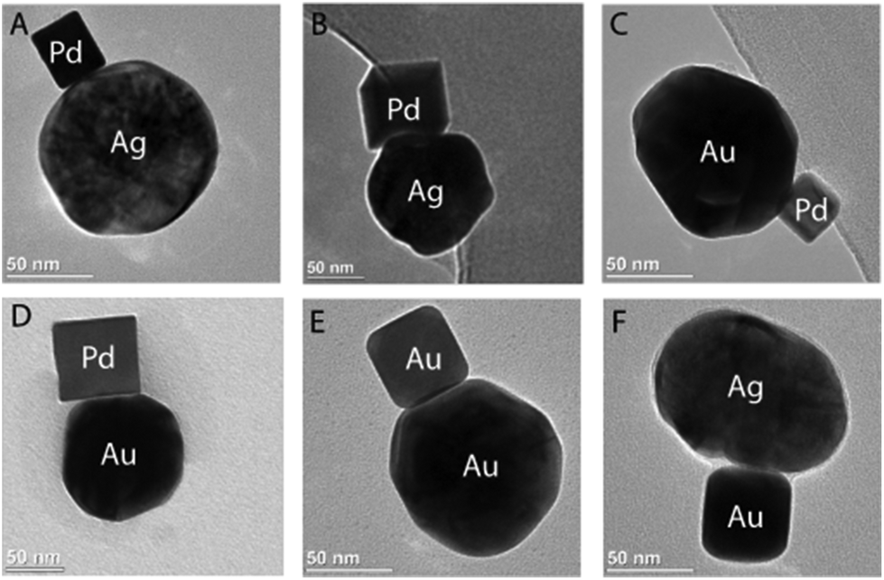 | ||
| Fig. 1 Noble metal nanoparticle heterodimers synthetized using non-covalent electrostatic self-assembly of colloids of different shapes, sizes, and materials: (A) Ag (spherical90 nm) and Pd (cube25 nm); (B) Ag (spherical90 nm) and Pd (cube70 nm); (C) Au (spherical90 nm) and Pd (cube25 nm); (D) Au (spherical90 nm) and Pd (cube70 nm); (E) Au (spherical90 nm) and Au (cube35 nm); (F) Ag (spherical90 nm) and Au (cube35 nm) (reproduced by ACS AuthorChoice – Open Access agreement from T. A. Gschneidtner, Y. A. D. Fernandez, S. Syrenova, F. Westerlund, C. Langhammer and K. Moth-Poulsen, Langmuir, 2014, 30(11), 3041–3050).86 | ||
Template driven self-assembly of NPs at interfaces and surfaces
One common limitation of the solution based self-assembly methods for building NP junctions is the inability to produce high yields of the tailored structures, requiring post-synthesis purification methods, that affect the actual yields. Additionally, purely solution-based single-molecule electronic devices are not feasible at the current state-of-the-art, and probably will never be conceived. Therefore, for applications, the methods based on self-assembly of proto-devices in solution will depend on micro- or nanofabrication techniques at surfaces, to guide and position nanoscale objects from solution to pre-determined, tailored sites. In this sense, the use of deterministic assembly of nanometric objects directly on engineered surfaces with controlled positioning and orientation can provide interesting paths for the bottom-up fabrication of devices.105–107Different experimental approaches have been proposed to combine self-assembly solution methods with solid-state architectures.44 The use of self-assembly methods at interfaces provides several advantages for the design and build-up of systems with low dimensionality (i.e. lower than 2). The interface between two environments of very different properties provides topological and energetic constrains that favour the emergence of supra-molecular structures with characteristics that might differ from the properties of bulk materials. Furthermore, thin films usually display high transmittance, relatively dynamic behaviour, and well-defined structural properties at different length scales. One promising strategy consists in the direct self-assembly of components at liquid–air interfaces, followed by subsequent transferring of these structures onto the surface of top-down fabricated electrodes. Following this strategy, Bjørnholm et al. succeeded with the fabrication of pseudo one-dimensional molecular electronic networks, consisting of segments of AuNPs separated by 1–3 nm wide gaps and interconnected by conjugated organic molecules.108 The networks were obtained by lipid templated self-assembly of AuNPs at the air–water interface. The Langmuir monolayer obtained was compressed and subsequently transferred horizontally (Langmuir–Schäfer) to a solid support with a prefabricated network of gold microelectrodes prepared by top-down UV/e-beam lithography. The electronic properties of this pseudo one-dimensional molecular electronic circuit were characterized by using macroscopic electrodes and a conductive AFM tip as the probe. This procedure can be easily adapted to any kind of molecular system having a strong affinity for the gold surface, while the entire circuit is built by a series of purely chemical manipulations under standard lab conditions.
A similar approach was applied to the preparation of ordered structures of gold AuNPs at the nanometer length scale, by using amphiphilic polymers as templating agents.109 The polymers used had a bi-functionalized poly(p-phenylene) backbone, with phenolic groups on one side and alkoxy chains on the other side, giving the polymer amphiphilic properties. These polymers are able to form stable mono- and multilayered Langmuir–(Blodgett/Schäfer) films by horizontal and vertical lifting.110–112 Furthermore, these polymeric molecules have interesting photophysical properties in solution and as solid films, making them good candidates as a template for self-organized nanostructures.112–114 The ability to control the morphology of the gold pattern by applying different surface pressures on the composite Langmuir film is a promising strategy for large-area self-assembly of architectures, useful to design complex molecular electronic devices.
The template structures used for the self-assembly of NPs can be directly built on solid surfaces, using top-down nanofabrication procedures. An interesting example of this strategy has been presented by Bjørnholm et al. demonstrating in situ growth of AuNRs with positional control and alignment in well-defined poly(methyl methacrylate) nanochannels.115 Spherical AuNPs were self-assembled at specific sites of the patterned substrates and the AuNRs were grown in situ using a seed-mediated synthetic approach (Fig. 2). The system allowed for fabrication of multiple nanogap junctions on a single chip with AuNRs acting as nanoelectrodes. The implementation of this method on surfaces pre-patterned with metallic electrodes is a promising strategy towards the development of parallel fabrication of single-molecule electronic devices. These results demonstrate the strength of combining top-down templating and bottom-up growth of electrically addressable devices. The top-down preparation of the metallic contacts prior to nanogap formation eliminates potential damage of the nanogap due to post-processing steps. The incorporation of π-conjugated systems prior to seeding leads to better control of the molecular orientation in the gaps, however some challenges remain in terms of yields of the devices.
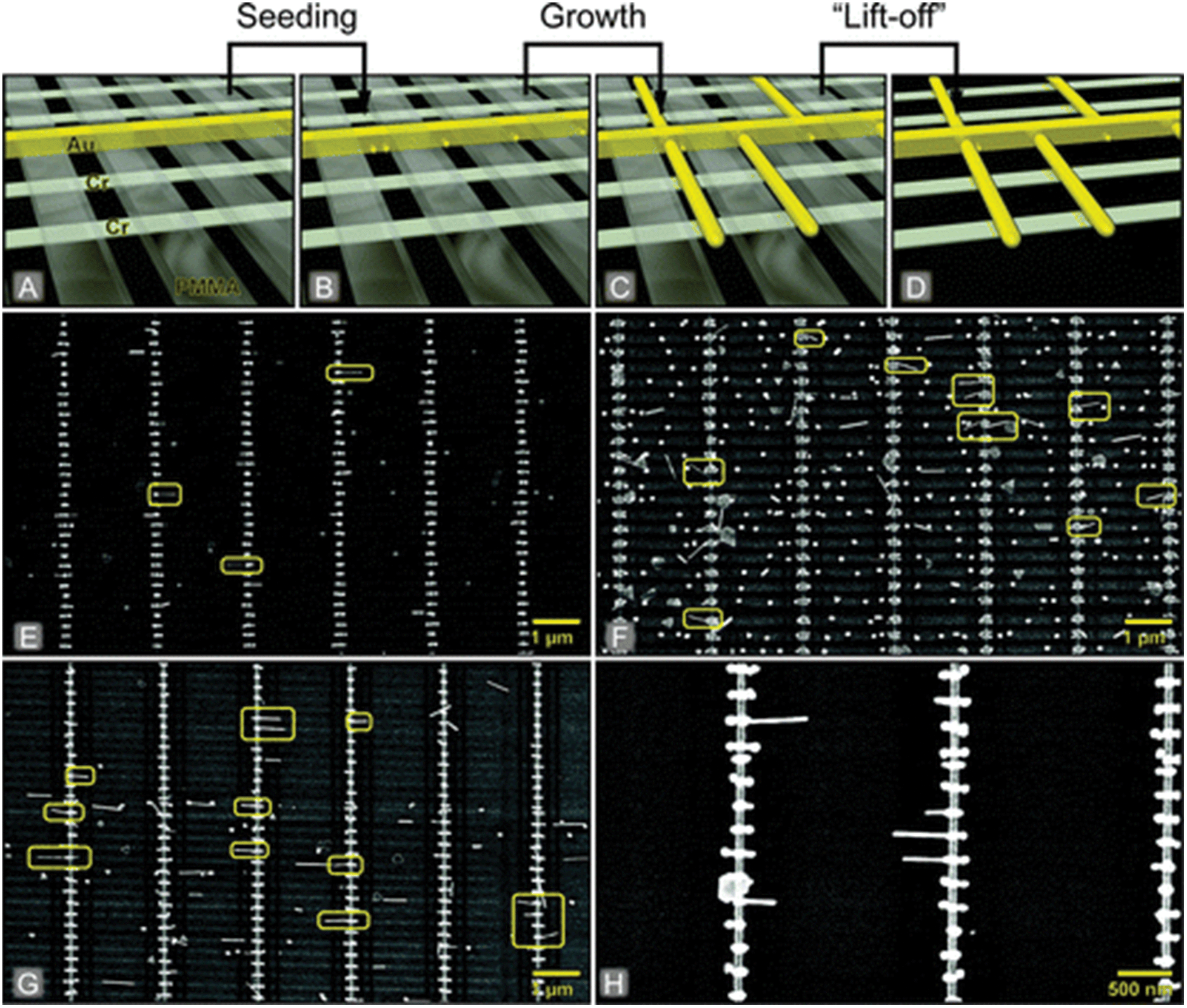 | ||
| Fig. 2 Schematic representation of stepwise assembly of nanoparticles (A and B) followed by in situ growth of nanorods (C) and removal of the directing PDMS template (D). (E–H) show SEM micrographs of successfully grown gold nanorods. Reprinted with permission from T. Jain, S. Lara-Avila, Y.-V. Kervennic, K. Moth-Poulsen, K. Nørgaard, S. Kubatkin, and T. Bjørnholm, ACS Nano, 2012, 6, 3861–3867. Copyright 2012 American Chemical Society.) | ||
An alternative, and very promising, strategy consists of the direct self-assembly of NPs within templates fabricated on surfaces. Extensive work carried out by Alivisatos et al., Wolf et al., and Vaia et al. has demonstrated the versatility of using capillarity forces combined with lithografically defined templates to drive the self-organization of NPs on nanoengineered surfaces.106,107,116–123 The incorporation of DNA-directed self-assembly methods on patterned surfaces has allowed further control of the morphology and orientation of the assembled structures,124,125 while the use of electrostatic trapping induced by surface topology has also been demonstrated.126
Recently, a top-down nanofabricated template has been combined with directed capillary assembly to place AuNRs in a highly deterministic pattern, forming continuous chains with dimensionality equal to unity.106 Within these straight chains, the AuNRs were aligned in one chosen direction with an end-to-end configuration. The precise control of the process leads to the formation of gaps of ∼6 nm between the individual constituents of the chain. The conditions for optimum quality and yield of AuNR chain assembly have been investigated, exploring the influence of template size and assembly temperature.106 This approach also allows the transfer of the self-assembled AuNR chains from the assembly template onto a Si/SiO2 target substrate, thus establishing a platform for a variety of nanoscale electronic and optical applications. A proof-of-principle experiment has been shown in these systems, performing electrical measurements on contacted AuNR chains before and after their immersion in a solution of thiol-end capped oligophenylenevinylene molecules. The increase in the conductance by three orders of magnitude in the presence of the conjugated oligomer indicates molecular-mediated charge transport across the nanogaps.106
Capillarity-assisted particle-assembly methods have become sophisticated, allowing the design and implementation of complex nanostructures with extremely high precision. One of the most impressive examples, presented by Wolf et al., has introduced the concept of cascade assembly to build-up complex patterns combining different kinds of nanoparticles.127
Capillary forces have also been used by Mirkin et al. to achieve shape selectivity during the self-assembly process,128 and to place segmented nanowires in well-defined bidimensional arrays.129
Despite the growing understanding of fundamental principles of capillary forces in confined nanostructures, the methods proposed for capilarity-driven self-assembly of NPs are often specific for the systems studied. Combining nanofabricated surfaces with capilary forces requires delicate tuning of several experimental variables, and allows precise control of the positioning of NPs after considerable experimental effort. In this sense the development of new general strategies to place NPs in pre-defined positions at surfaces, avoiding topological constrains, would be a breakthrough in this research field.
NP positioning by electrostatic soft-template directed self-assembly
A relevant challenge when assembling nanopartilces on solid surfaces is the selectivity and the control of the NP adhesion in specific patterns and at preferred locations on the surface, especially to be able to control adhesion and thereby the sites where nanoscale objects are positioned. Microspheres have been successfully self-assembled on patterned structures, and the factors controlling the self-organization of these objects have been studied.130,131 Several methods for controlled positioning of NPs on surfaces have also been investigated.132,133 One interesting approach is based on the electrophoretic deposition of NPs on pre-patterned surfaces.134–136 This method allows faster processing times with respect to other deposition techniques.137 Capilary forces, discussed in the previous section, have been combined with top-down nanofabricated templates to control orientation and positiong of NPs on surfaces.106,107,116–129 Selective chemical functionalization of surfaces has also been used to drive the self-assembly of NPs exploiting the chemistry of silane-derivatives on Si surfaces138–140 and using micro-contact printing on gold surfaces.141Direct surface self-assembly methods are versatile and allow the development of more advanced procedures to increase the control of nanostructure positioning and topographical orientation of small objects. At the current state-of-the-art, the highest control over NPs orientation and positioning can be achieved by the combination of top-down engineering of surfaces and bottom-up self-assembly methods.127,129
Efficient top-down methods for the fabrication of electrodes and complex surface patterns have become available in the last decades, and the considerable improvement of spatial resolution and large-area reliability of these techniques has contributed to the development of different research areas.142
Exploiting the distinctive chemical properties of Si- and metal-based surfaces, it has been possible to build self-assembled sub-monolayers of NPs with well-defined structural properties. The possibility of exploiting non-covalent interactions to direct the self-assembly of NP monolayers is very attractive, since it takes advantage of collective interactions responsible for the properties of supramolecular systems.
The strategy we present here is based on a silane-free versatile method able to address the challenge of NP selective positioning based on the direct self-assembly of NPs from colloidal solutions on nanofabricated oxidized Si surfaces, avoiding the use of capillarity interactions and without external electrophoretic fields. As it will be shown below, we have used self-assembled lipid bilayers as a soft template to reduce unspecific binding of NPs to material-specific areas of the surface. This method allows controlled self-assembly and selective positioning of objects with nanometric space-resolution using a general strategy that we envision to easily extend to different kinds of surface materials and NPs.
SiO2 surfaces are well known to promote non-covalent adsorption of positively charge molecules and NPs. This capacity can be used to form homogeneous self-assembled sub-monolayers of metal NPs capped with cationic surfactants. Several methods for the synthesis of shaped metal NPs involve cationic amphiphilic molecules as stabilizers of specific crystallographic facets on the metal surface.28,143–149 The removal or exchange of these surfactant molecules from the particle surface after the synthesis, without compromising the stability of the colloids, is a challenging task.28,86
We have observed a general self-assembly behaviour on SiO2 or oxidized Si substrates for several NP systems stabilized by cationic surfactants, irrespectively of the shape, the size or the material of the NPs (Fig. 3a,b; and ESI SI2, SI3†). The NPs used for these experiments were synthetized by methods previously reported, that introduce cetyltrimethyl ammonium bromide or chloride as capping agents (further details as ESI SI1†).28,144–146 These synthetic routes yield NPs with low dispersity in terms of shape and size. The introduction of the cationic surfactants provides a net positive charge on the surface of the colloids. We have successfully formed self-assembled sub-monolayers of Pd nanocubes, Au nanocubes, and Au rhombic dodecahedra NPs of different sizes, on oxidized Si surfaces, demonstrating the versatility of this approach (SEM images of representative examples of NP sub-monolayers are presented in Fig. 3 and in ESI†).
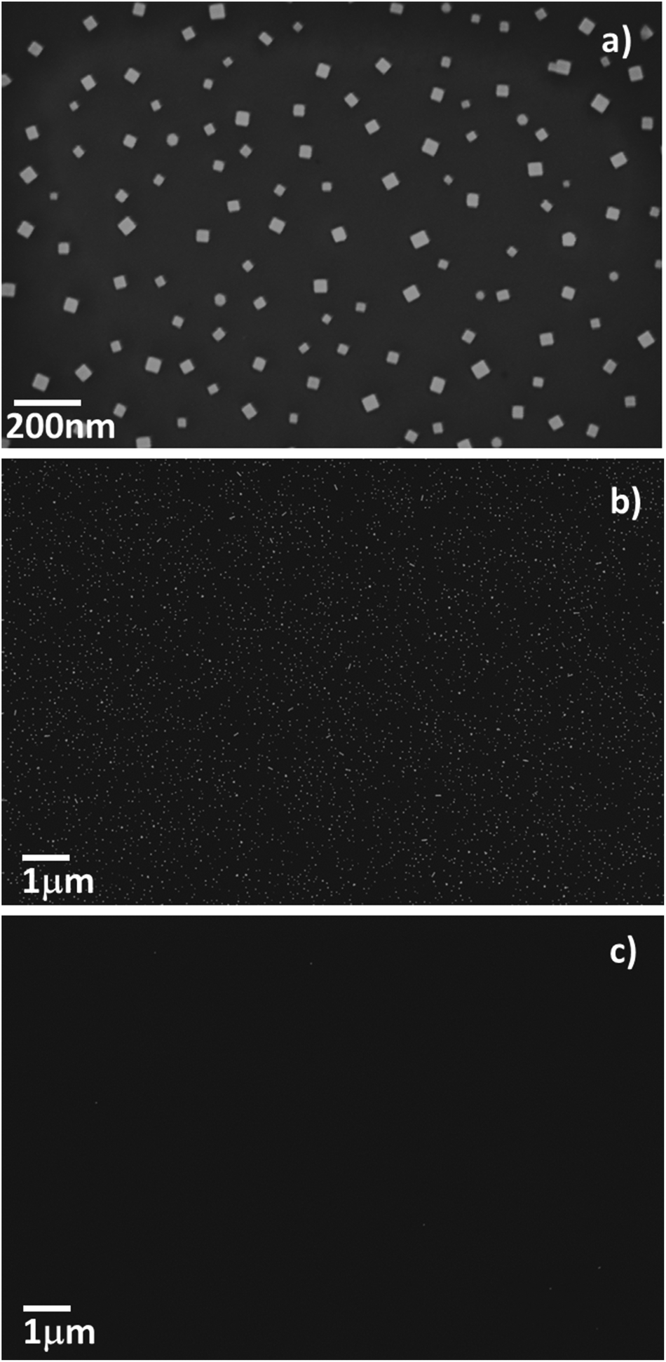 | ||
| Fig. 3 Self-assembled NP sub-monolayer on oxidized Si surfaces: (a, b) PdNPs (25 nm) on clean oxidized Si surfaces at different magnifications; (c) Lipid bilayer passivation preventing PdNP sub-monolayer formation on Si surface. | ||
The process used for the preparation of the NP sub-monolayers is based on drop-casting on clean oxidized Si surfaces, followed by incubation in solutions for 30 minutes, and rinsing with deionized water. The surface of the Si wafer was cleaned with oxygen plasma before use, but also other kinds of oxidative cleaning procedures, such as piranha etching or thermal annealing, are effective for this deposition technique. The procedure leads to homogeneous sub-monolayers of NPs evenly distributed on the surface of oxidized Si wafers. These NP sub-monolayers were stable after rinsing with water as well as with organic solvents (see SI4† for further details).
On the other hand, the surface properties of oxidized Si substrates can be modified to control the adhesion on the particles to the surface. We have previously shown that surface passivation by coating with lipid bilayers almost completely eliminates the non-specific adhesion of biomolecules and NPs within SiO2 nanochannels.151 The lipid-surface passivation method has been demonstrated to perform better than standard passivation protocols, i.e. bovine serum albumin (BSA) coating. This approach has also the advantage of self-healing, which is a typical characteristic of supramolecular systems that allows the self-assembled structure to correct intrinsic or induced defects by exchange of molecules with the solution and rearrangement on the surface. Freely moving quantum dots, proteins and protein–DNA complexes have been successfully studied in devices passivated with lipids, preventing interference of non-specific chemisorption.150,151
The presence of self-assembled lipid bilayers on the surface of SiO2 drastically prevents the adsorption of the NPs investigated in this work. The surface density of NPs is decreased by more than two orders of magnitude in the presence of the bilayers (Fig. 3c), with respect to the clean SiO2 surface (Fig. 3b). This non-covalent passivation strategy is relatively simple, did not compromise the surface properties of the substrate on a permanent basis, and results in a promising strategy for the self-assembly of nanoscale devices on surfaces.
When using lipid bilayers on flat surfaces, there are two major experimental challenges to overcome: the lateral diffusion of the bilayers on open surfaces and the requirement of a continuously wet environment. We spread lipid bilayer liposomes, 100 nm in diameter, on the oxidized Si surface to spontaneously form self-assembled bilayers. These structures require a mechanical barrier to contain the lateral diffusion of the lipids on the flat surface, and for this reason, before the wet functionalization, we fabricated a PMMA pool on the edge of the oxidized Si surface, that provides mechanical stability to the lipid bilayer, and also acts as container for the droplet of solution on top of the clean oxidized Si surface. Within this pool, the solutions are exchanged using source and drain pipettes simultaneously, in order to avoid the bilayer-functionalized surface to get dry. Following this procedure it is possible to substitute the previous solution with a new one, allowing the change of buffer solutions, rinsing the surface, and removing the colloidal solutions, without affecting the stability of the lipid bilayers on the oxidized Si surface.
The solutions were exchanged gradually, and equilibration was allowed between one functionalization and the next. The substrates were initially rinsed with the same buffer solution used to store the liposomes, and when the liposomes were introduced on the surface, 15 minutes of stabilization time was allowed. The lipid solution was rinsed first with liposome buffer and thereafter with water, before introducing the colloidal solutions. When needed, several rinsing steps were performed in order to completely remove the residues from the previous solution. After rinsing the NP solution, the surface can be dried, plasma cleaned, and analysed using SEM (Fig. 3). The full description of the preparation of NP sub-monolayers is provided as ESI (ESI1 and Fig. S1†).
The adhesion of charged NPs to the surface can also be tailored by adjusting the surface potential of metal surfaces.152 We have used chemisorption of charged molecules on Au surfaces to change the surface charge. Gold has particular affinity for thiols, and the properties of self-assembled molecular monolayers of thiols on noble metal surfaces have been extensively studied.153–158 We could not observe the formation of self-assembled sub monolayers of metal NPs stabilized by cationic surfactants on clean gold surfaces (Fig. 4a), while gold surfaces functionalized with sulfonate groups promote the adhesion of positively charged NPs (Fig. 4b). These distinctive properties can be exploited for non-covalent self-assembly of more complex NP architectures and devices, and to interface bottom-up self-assembled proto-devices with top-down fabricated nano- and micro-structures.27
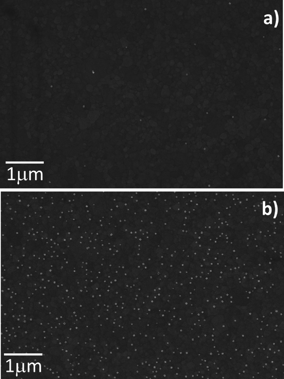 | ||
| Fig. 4 Self-assembled sub-monolayer of PdNPs (25 nm): (a) on plasma-cleaned gold surface; (b) on gold surface functionalized with MESNa. | ||
Direct self-assembly methods can be used to control the placement of NPs on nano-engineered surfaces, and to modify the morphology of NP monolayers. Similarly, lipid bilayers can drive the formation of self-assembled monolayers on selected areas of nanofabricated surfaces. Combining these two complementary features, we have been able to build up prototypes of self-assembled plasmonic sensors based on nanofabricated gold disks linked to palladium NPs (Fig. 5d). The gold disks were nanofabricated on SiO2 surfaces using Hole-Mask Colloidal Lithography.159 A 5 nm thick Cr layer was used to improve the adhesion of the Au-structures to the oxidized Si-surface. As discussed above, CTAB stabilized PdNPs are able to form sub-monolayers on the surface of the SiO2, and therefore they are spread evenly on the nanofabricated plasmonic surfaces (Fig. 5a), and only 15% of the Au structures are in contact with PdNPs. When the Au-surface is functionalized with the negatively charged thiol–sulfonate molecules (sodium 2-mercaptoethanesulfonate, MESNa), the self-assembly of positively charged PdNPs is preferentially driven towards the Au surface, allowing more than 99% of the Au-disks to host PdNPs, but still non-specific adsorption is observed on the oxidized Si surface (Fig. 5b). The combination of lipid-passivation with functionalization of Au with MESNa leads to the exclusive positioning of PdNPs on 56% of the Au structures, effectively preventing adhesion to oxidized Si-surfaces (Fig. 5d). When the lipid passivation was used without MESNa on Au (Fig. 5c), less than 5% of the Au-structures were occupied by PdNPs, therefore the combination of MESNa-functionalization on gold and lipid-bilayer passivation on oxidized Si is essential for driving the self-assembly towards the Au-structures.
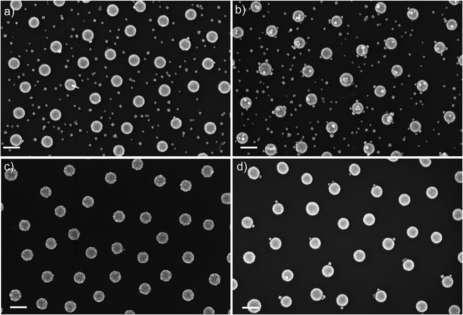 | ||
| Fig. 5 Representative examples of self-assembled sub-monolayers of PdNPs (25 nm) on plasma-cleaned top-down nanofabricated Au-disks on oxidized Si surface: (a) clean surface; (b) Au functionalized with MESNa; (c) SiO2 passivated by self-assembled lipid bilayer; (d) SiO2 passivated by self-assembled lipid bilayer and Au functionalized with MESNa. Scale bars are 200 nm. | ||
This step-wise functionalization approach allows us to selectively modify the surface properties of oxidized Si and Au, exploiting the specific interactions of surface active species on different materials. The strategy developed, similar to the approach used on oxidized Si wafers, also requires the continuous and smooth exchange of solutions on top of the nanofabricated structures, in order to avoid drying and preserve the structural integrity of the lipid bilayers (Fig. 6). In this case, we have also used the PMMA pool on the edge of the wafer. The top-down nanofabricated Au structures were functionalized with MESNa (Fig. 6b), keeping the surface in contact with the solution (6 × 10⁻⁵ M of MESNa in water) for 2 hours before rinsing with water (Fig. 6c). The subsequent steps (Fig. 6c–h) were performed following the procedure described above for flat oxidized Si substrates. The self-assembled structures are stable upon drying and plasma cleaning, allowing SEM characterization (Fig. 5).
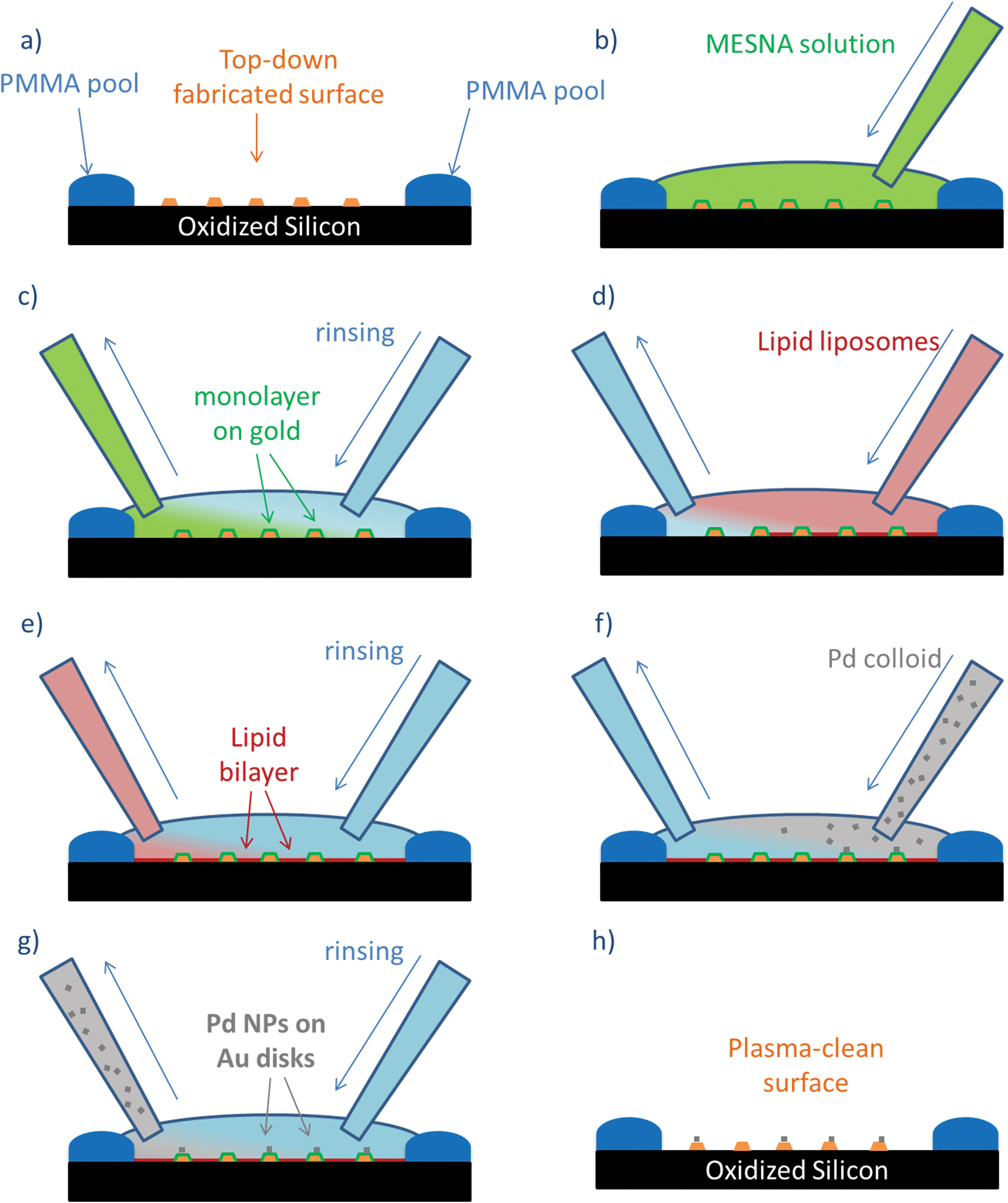 | ||
| Fig. 6 Schematic representation of the layer-by-layer strategy used for the functionalization of top-down nanofabricated structures: (a) starting surface, (b–c) MESNa functionalization of Au surface; (d–e) SiO2 passivation with lipid bilayers; (f–g) colloidal deposition; (h) final surface. | ||
To further demonstrate the control of the positioning of PdNPs on oxidized Si surfaces, we explored other geometrical shapes of gold patches. Specifically, we used oxidized Si wafers onto which gold lines were patterned using e-beam lithography (Fig. 7). The selectivity of NP self-assembly was again achieved by lipid-bilayer passivation of the SiO2 surface, and functionalization of the Au-structures with MESNa, following the strategy depicted in Fig. 6. This electrostatic soft-template directed self-assembly method allows highly selective self-assembly of PdNPs on the Au-surface, producing a surface density of PdNPs on gold that is 4000 times greater compared to that on the SiO2 surface.
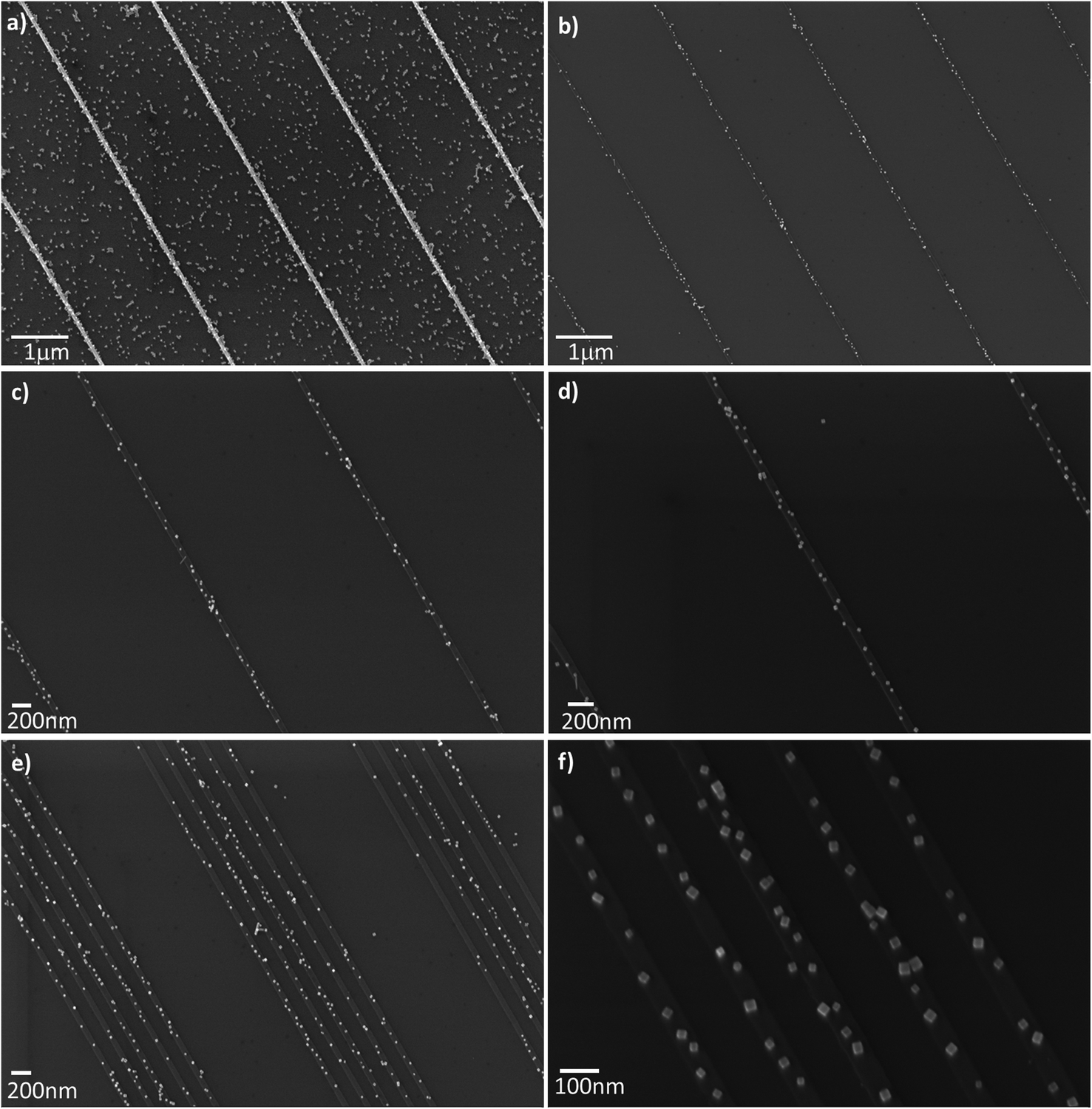 | ||
| Fig. 7 PdNPs self-assembled on gold top-down fabricated structures: (a) clean Au lines patterns on clean oxidized Si wafer, (b–f) MESNa functionalized Au-lines pattern on oxidized Si lipid-bilayer passivated wafer (different magnifications, and different patterns). | ||
Probably the most relevant strength of the non-covalent self-assembly methods presented here is illustrated in the low magnification SEM images in Fig. 7b and 7e, showing scalability from small to large area devices. This capacity combined with the versatility of deterministic assembly procedures allows simultaneous fabrication of several independent devices on macroscopic surfaces.
Concluding remarks
The impressive development of supra-molecular chemistry and self-assembly methods in the last decades has contributed to the establishment of a well-structured experimental and conceptual framework that provides promising routes for the design of advanced functional structures such as single molecule electronic devices, nano-actuators and nano-machines. Many examples of functional nano-devices are assembled, fabricated, or deposited on macroscopic electrodes or bulk substrates. This dichotomy seems to be intrinsic in nature and there is no obvious shortcut to bypass it at the current state-of-the-art.In recent years the research community has begun to exploit the combination of “bottom-up” & “top-down” approaches, finding paths to merge these two strategies efficiently. The challenge of developing reliable methods to produce large scale arrays of nano devices connected in circuit-like architectures is not solved yet, and one can foresee that this will be an exciting research topic for the coming years. The combination of soft-matter masks with metal and metal oxide NP chemical and physical synthesis might lead to unexpected scientific breakthroughs. Such breakthroughs might be associated with template-free self-assembly methods, able to be scaled-up to large surfaces.
The different strategies discussed here, developed by our group and by others, and chronologically distributed over the last 10 years, show a trend towards in situ integration of self-assembly and top-down approaches to control the position and orientation of nanometric objects on functional surfaces. Several technological and scientific challenges can be addressed by the complementary merging of top-down and bottom-up methods that, at the current state-of-the-art, would only be feasible on supporting macroscopic substrates. Among these approaches, the soft-template directed self-assembly method, presented in the last section of this work, offers several advantages in terms of versatility and simplicity. We have been able to control NP positioning on nano-structured surfaces with high precision with the use of tools available in any wet-chemistry laboratory, and following reproducible procedures that can be easily scaled-up and adapted to different kinds of NPs and substrates with little experimental effort. This approach also provides a versatile path for in situ build-up of complex nanostructures combining NPs of different materials that have been already used for plasmonic sensing of catalytic reactions at the nanoscale.86,91–93 Furthermore, these bimetallic systems can be also used as model systems for plasmon-enhanced catalysis,94–103 and thermo-electric power generation.104
Acknowledgements
This work was funded by the Areas of Advance in Materials Science and in Nanoscience and Nanotechnology at Chalmers University of Technology. KMP acknowledges the financial support of the ERC Starting Grant SIMONE. FW acknowledges funding from the Swedish Research Council (project no 2011–4324).Notes and references
- R. L. McCreery, H. Yan and A. J. Bergren, Phys. Chem. Chem. Phys., 2013, 15, 1065–1081 RSC.
- H. D. Yu, M. D. Regulacio, E. Ye and M. Y. Han, Chem. Soc. Rev., 2013, 42(14), 6006–6018 RSC.
- A. Biswas, I. S. Bayer, A. S. Biris, T. Wang, E. Dervishi and F. Faupel, Adv. Colloid Interface Sci., 2012, 170(1), 2–27 CrossRef CAS PubMed.
- D. Mijatovic, J. C. T. Eijkel and A. Van Den Berg, Lab Chip, 2005, 5(5), 492–500 RSC.
- T. J. Merkel, K. P. Herlihy, J. Nunes, R. M. Orgel, J. P. Rolland and J. M. DeSimone, Langmuir, 2009, 26(16), 13086–13096 CrossRef PubMed.
- W. Lu and C. M. Lieber, Nat. Mater., 2007, 6(11), 841–850 CrossRef CAS PubMed.
- J. Melin and S. R. Quake, Annu. Rev. Biophys. Biomol. Struct., 2007, 36, 213–231 CrossRef CAS PubMed.
- S. Takahashi, K. Suzuki, M. Okano, M. Imada, T. Nakamori, Y. Ota and S. Noda, Nat. Mater., 2009, 8(9), 721–725 CrossRef CAS PubMed.
- D. A. Canelas, K. P. Herlihy and J. M. DeSimone, Wiley Interdiscip. Rev.: Nanomed. Nanobiotechnol., 2009, 1(4), 391–404 CrossRef CAS PubMed.
- J. V. Barth, G. Costantini and K. Kern, Nature, 2005, 437(7059), 671–679 CrossRef CAS PubMed.
- R. W. Keyes, IBM J. Res. Dev., 2000, 44(12), 84–88 CrossRef.
- W. Göpel, Sens. Actuators, A, 1996, 56(1), 83–102 CrossRef.
- Lloyd R. Harriott, Proc. IEEE, 2001, 89(3), 366–374 CrossRef.
- Y. Wang and Y. Xia, Nano Lett., 2004, 4(10), 2047–2050 CrossRef CAS.
- J. M. Lehn, Proc. Natl. Acad. Sci. U. S. A., 2002, 99(8), 4763–4768 CrossRef CAS PubMed.
- S. Zhang, Nat. Biotechnol., 2003, 21, 1171–1178 CrossRef CAS PubMed.
- J. M. Lehn, Angew. Chem., Int. Ed. Engl., 1990, 29(11), 1304–1319 CrossRef PubMed.
- J. M. Lehn, Eur. Rev., 2009, 17(02), 263–280 CrossRef.
- Janos H. Fendler, Chem. Mater., 1996, 8(8), 1616–1624 CrossRef CAS.
- S. Flink, F. C. J. M. van Veggel and D. N. Reinhoudt, Adv. Mater., 2000, 12, 1315–132821 CrossRef CAS.
- M.-P. Pileni, Acc. Chem. Res., 2007, 40(8), 685–693 CrossRef CAS PubMed.
- P. W. Rothemund, Nature, 2006, 440(7082), 297–302 CrossRef CAS PubMed.
- J. Y. Cheng, A. M. Mayes and C. A. Ross, Nat. Mater., 2004, 3(11), 823–828 CrossRef CAS PubMed.
- W. M. Tolles, MRS Bull., 2000, 25(10), 36–38 CrossRef.
- A. Kumar, H. A. Biebuyck and G. M. Whitesides, Langmuir, 1994, 10(5), 1498–1511 CrossRef CAS.
- C. Gerber and H. P. Lang, Nat. Nanotechnol., 2006, 1(1), 3–5 CrossRef CAS PubMed.
- Y. D. Fernandez, L. Sun, T. Gschneidtner and K. Moth-Poulsen, APL Mater., 2014, 2(1), 010702 CrossRef PubMed.
- T. A. Gschneidtner, Y. A. D. Fernandez and K. Moth-Poulsen, J. Mater. Chem. C, 2013, 1(43), 7127–7133 RSC.
- G. Molnár, S. Cobo, J. A. Real, F. Carcenac, E. Daran, C. Vieu and A. Bousseksou, Adv. Mater., 2007, 19(16), 2163–2167 CrossRef PubMed.
- R. G. Hobbs, N. Petkov and J. D. Holmes, Chem. Mater., 2012, 24(11), 1975–1991 CrossRef CAS.
- J. Zhang, Y. Li, X. Zhang and B. Yang, Adv. Mater., 2010, 22, 4249–4269 CrossRef CAS PubMed.
- R. J. Kershner, L. D. Bozano, C. M. Micheel, A. M. Hung, A. R. Fornof, J. N. Cha, C. T. Rettner, M. Bersani, J. Frommer, P. W. K. Rothemund and G. M. Wallraff, Nat. Nanotechnol., 2009, 4(9), 557–561 CrossRef CAS PubMed.
- E. Pibiri, P. Holzmeister, B. Lalkens, G. P. Acuna and P. Tinnefeld, Nano Lett., 2014, 14(6), 3499–3503 CrossRef CAS PubMed.
- R. Krahne, A. Yacoby, H. Shtrikman, I. Bar-Joseph, T. Dadosh and J. Sperling, Appl. Phys. Lett., 2002, 81(4), 730–732 CrossRef CAS PubMed.
- A. Guttman, D. Mahalu, J. Sperling, E. Cohen-Hoshen and I. Bar-Joseph, Appl. Phys. Lett., 2011, 99(6), 063113 CrossRef PubMed.
- Y. Vardi, A. Guttman and I. Bar-Joseph, Nano Lett., 2014, 14(5), 2794–2799 CrossRef CAS PubMed.
- T. Dadosh, Y. Gordin, R. Krahne, I. Khivrich, D. Mahalu, V. Frydman, J. Sperling, A. Yacoby and I. Bar-Joseph, Nature, 2005, 436, 677–680 CrossRef CAS PubMed.
- A. Bezryadin, C. Dekker and G. Schmid, Appl. Phys. Lett., 1997, 71(9), 1273–1275 CrossRef CAS PubMed.
- C. Sönnichsen, B. M. Reinhard, J. Liphardt and A. P. Alivisatos, Nat. Biotechnol., 2005, 23(6), 741–745 CrossRef PubMed.
- G. Chen, Y. Wang, L. H. Tan, M. Yang, L. S. Tan, Y. Chen and H. Chen, J. Am. Chem. Soc., 2009, 131(12), 4218–4219 CrossRef CAS PubMed.
- J. P. Novak and D. L. Feldheim, J. Am. Chem. Soc., 2000, 122(16), 3979–3980 CrossRef CAS.
- R. Sardar, T. B. Heap and J. S. Shumaker-Parry, J. Am. Chem. Soc., 2007, 129(17), 5356–5357 CrossRef CAS PubMed.
- W. Li, P. H. Camargo, X. Lu and Y. Xia, Nano Lett., 2008, 9(1), 485–490 CrossRef PubMed.
- K. Moth-Poulsen and T. Bjørnholm, Nat. Nanotechnol., 2009, 4(9), 551–556 CrossRef CAS PubMed.
- J. Kumar, X. Wei, S. Barrow, A. M. Funston, K. G. Thomas and P. Mulvaney, Phys. Chem. Chem. Phys., 2013, 15, 4258–4264 RSC.
- L. Wang, Y. Zhu, L. Xu, W. Chen, H. Kuang, L. Liu, A. Agarwal, C. Xu and N. A. Kotov, Angew. Chem., Int. Ed., 2010, 49(32), 5472–5475 CrossRef CAS PubMed.
- L. Zhong, X. Zhou, S. Bao, Y. Shi, Y. Wang, S. Hong, Y. Huang, X. Wang, Z. Xie and Q. Zhang, J. Mater. Chem., 2011, 21, 14448–14455 RSC.
- Y. Wang, Y. Li Fang, J. Wang, Y. Sang and C. Zhi Huang, Chem. Commun., 2010, 46, 1332–1334 RSC.
- T. Jain, Q. Tang, T. Bjørnholm and K. Nørgaard, Acc. Chem. Res., 2014, 47(1), 2–11 CrossRef CAS PubMed.
- H. Li, Z. Li, L. Wu, Y. Zhang, M. Yu and L. Wei, Langmuir, 2013, 29, 3943–3949 CrossRef CAS PubMed.
- K.-M. Sung, D. W. Mosley, B. R. Peelle, S. Zhang and J. M. Jacobson, J. Am. Chem. Soc., 2004, 126, 5064–5065 CrossRef CAS PubMed.
- Y. Wei, K. J. M. Bishop, J. Kim, S. Soh and B. A. Grzybowski, Angew. Chem., Int. Ed., 2009, 48, 9477–9480 CrossRef CAS PubMed.
- P. M. Peiris, E. Schmidt, M. Calabrese and E. Karathanasis, PLoS One, 2011, 6, e15927 CAS.
- J. G. Worden, A. W. Shaffer and Q. Huo, Chem. Commun., 2004, 518–551 RSC.
- D. Nepal, K. Park and R. A. Vaia, Small, 2012, 8, 1013–1020 CrossRef CAS PubMed.
- M. Grzelczak, A. Sánchez-Iglesias, H. H. Mezerji, S. Bals, J. Pérez-Juste and L. M. Liz-Marzán, Nano Lett., 2012, 12, 4380–4384 CrossRef CAS PubMed.
- B. Dong, B. Li and C. Y. Li, J. Mater. Chem., 2011, 21, 13155–13158 RSC.
- S. Pradhan, D. Ghosh and S. Chen, ACS Appl. Mater. Interfaces, 2009, 1, 2060–2065 CAS.
- A. Hofmann, P. Schmiel, B. Stein and C. Graf, Langmuir, 2011, 27, 15165–15175 CrossRef CAS PubMed.
- A. P. Alivisatos, K. P. Johnsson, X. Peng, T. E. Wilson, C. J. Loweth, M. P. Bruchez and P. G. Schultz Jr., Nature, 1996, 382, 609–611 CrossRef CAS PubMed.
- B. M. Reinhard, M. Siu, H. Agarwal, A. P. Alivisatos and J. Liphardt, Nano Lett., 2005, 5, 2246–2252 CrossRef CAS PubMed.
- P. K. Jain, W. Huang and M. A. El-Sayed, Nano Lett., 2007, 7, 2080–2088 CrossRef CAS.
- T. Sannomiya, C. Hafner and J. Voros, Nano Lett., 2008, 8, 3450–3455 CrossRef CAS PubMed.
- Y. Li, C. Jing, Y. Zhang and Y.-T. Long, Chem. Soc. Rev., 2012, 41, 632–642 RSC.
- B. M. Reinhard, S. Sheikholeslami, A. Mastroianni, A. P. Alivisatos and J. Liphardt, Proc. Natl. Acad. Sci. U. S. A., 2007, 104, 2667–2672 CrossRef CAS PubMed.
- S. E. Lee, A. P. Alivisatos and M. J. Bissell, Syst. Biomed., 2013, 1–9 Search PubMed.
- M. P. Busson, B. Rolly, B. Stout, N. Bonod, E. Larquet, A. Polman and S. Bidault, Nano Lett., 2011, 11, 5060–5065 CrossRef CAS PubMed.
- X. Lan, Z. Chen, B.-J. Liu, B. Ren, J. Henzie and Q. Wang, Small, 2013, 9, 2308–2315 CrossRef CAS PubMed.
- M. M. Maye, M. T. Kumara, D. Nykypanchuk, W. B. Sherman and O. Gang, Nat. Nanotechnol., 2010, 5, 116–120 CrossRef CAS PubMed.
- I. A. Trantakis, S. Bolisetty, R. Mezzenga and S. J. Sturla, Langmuir, 2013, 29, 10824–10830 CrossRef CAS PubMed.
- C. Chi, F. Vargas-Lara, A. V. Tkachenko, F. W. Starr and O. Gang, ACS Nano, 2012, 6, 6793–6802 CrossRef CAS PubMed.
- L. Lermusiaux, A. Sereda, B. Portier, E. Larquet and S. Bidault, ACS Nano, 2012, 6, 10992–10998 CAS.
- Y.-S. Chen, M.-Y. Hong and G. S. Huang, Nat. Nanotechnol., 2012, 7, 197–203 CrossRef CAS PubMed.
- J. I. L. Chen, H. Durkee, B. Traxler and D. S. Ginger, Small, 2011, 7, 1993–1997 CrossRef CAS PubMed.
- J. I. L. Chen, Y. Chen and D. S. Ginger, J. Am. Chem. Soc., 2010, 132, 9600–9601 CrossRef CAS PubMed.
- W. Ma, M. Sun, L. Xu, L. Wang, H. Kuang and C. Xu, Chem. Commun., 2013, 49, 4989–4991 RSC.
- R. J. Macfarlane, M. N. O'Brien, S. H. Petrosko and C. A. Mirkin, Angew. Chem., Int. Ed., 2013, 52, 5688–5698 CrossRef CAS PubMed.
- C. M. Galloway, M. P. Kreuzer, S. S. Acimovic, G. Volpe, M. Correia, S. B. Petersen, M. T. Neves-Petersen and R. Quidant, Nano Lett., 2013, 13, 4299–4304 CrossRef CAS PubMed.
- X. Wang, G. Li, T. Chen, M. Yang, Z. Zhang, T. Wu and H. Chen, Nano Lett., 2008, 8, 2643–2647 CrossRef CAS PubMed.
- Y. Zhang, Z. Zhao, D. Fracasso and R. C. Chiechi, Isr. J. Chem., 2014, 54, 513–533 CrossRef CAS PubMed.
- G. Chen, Y. Wang, M. Yang, J. Xu, S. J. Goh, M. Pan and H. Chen, J. Am. Chem. Soc., 2010, 132, 3644–3645 CrossRef CAS PubMed.
- L. V. Brown, H. Sobhani, J. B. Lassiter, P. Nordlander and N. J. Halas, ACS Nano, 2010, 4, 819–832 CrossRef CAS PubMed.
- S. Bidault, F. J. G. Abajo and A. De Polman, Plasmon-Based Nanolenses Assembled on a Well-Defined DNA Template, J. Am. Chem. Soc., 2008, 130, 2750–2751 CrossRef CAS PubMed.
- A. Lombardi, M. P. Grzelczak, A. Crut, P. Maioli, I. Pastoriza-Santos, L. M. Liz-Marzán, N. Del Fatti and F. Vallée, ACS Nano, 2013, 7, 2522–2531 CrossRef CAS PubMed.
- S. Sheikholeslami, Y.-W. Jun, P. K. Jain and A. P. Alivisatos, Nano Lett., 2010, 10, 2655–2660 CrossRef CAS PubMed.
- T. A. Gschneidtner, Y. A. D. Fernandez, S. Syrenova, F. Westerlund, C. Langhammer and K. Moth-Poulsen, Langmuir, 2014, 30(11), 3041–3050 CrossRef CAS PubMed.
- S. Karthäuser, J. Phys.: Condens. Matter, 2011, 23, 013001 CrossRef PubMed.
- M. C. Lennartz, N. Atodiresei, V. Caciuc and S. Karthäuser, J. Phys. Chem. C, 2011, 115(30), 15025–15030 CAS.
- M. C. Lennartz, M. Baumert, S. Karthäuser, M. Albrecht and R. Waser, Langmuir, 2011, 27(16), 10312–10318 CrossRef CAS PubMed.
- N. Babajani, P. Kowalzik, R. Waser, M. Homberger, C. Kaulen, U. Simon and S. Karthäuser, J. Phys. Chem. C, 2013, 117(42), 22002–22009 CAS.
- N. Liu, M. L. Tang, M. Hentschel, H. Giessen and A. P. Alivisatos, Nat. Mater., 2011, 10, 631–636 CrossRef CAS PubMed.
- T. Shegai, P. Johansson, C. Langhammer and M. Käll, Nano Lett., 2012, 12, 2464–2469 CrossRef CAS PubMed.
- E. M. Larsson, C. Langhammer, I. Zorić and B. Kasemo, Science, 2009, 326, 1091–1094 CrossRef CAS PubMed.
- Y. Tang, Z. Jiang, Q. Tay, J. Deng, Y. Lai, D. Gong, Z. Dong and Z. Chen, RSC Adv., 2012, 2, 9406–9414 RSC.
- Z. Zhang, L. Chen, M. Sun, P. Ruan, H. Zhengb and H. Xu, Nanoscale, 2013, 5, 3249–3252 RSC.
- K. Awazu, M. Fujimaki, C. Rockstuhl, J. Tominaga, H. Murakami, Y. Ohki, N. Yoshida and T. Watanabe, J. Am. Chem. Soc., 2008, 130, 1676–1680 CrossRef CAS PubMed.
- J. Chen, J. C. S. Wu, P. C. Wu and D. P. Tsai, J. Phys. Chem. C, 2011, 115, 210–216 CAS.
- X. Huang, Y. Li, Y. Chen, H. Zhou, X. Duan and Y. Huang, Angew. Chem., Int. Ed., 2013, 52, 6063–6067 CrossRef CAS PubMed.
- A. Tanaka, Y. Nishino, S. Sakaguchi, T. Yoshikawa, K. Imamura, K. Hashimoto and H. Kominami, Chem. Commun., 2013, 49, 2551–2553 RSC.
- Z. Zhang, M. Sun, P. Ruan, H. Zheng and H. Xu, Nanoscale, 2013, 5, 4151–4155 RSC.
- Z. Zhang, S. Sheng, H. Zheng, H. Xu and M. Sun, Nanoscale, 2014, 6, 4903 RSC.
- Y. Tang, Z. Jiang, G. Xing, A. Li, P. D. Kanhere, T. C. Sum, S. Li, X. Chen, Z. Dong and Z. Chen, Adv. Funct. Mater., 2013, 23, 2932–2940 CrossRef CAS PubMed.
- S. Linic, P. Christopher and D. B. Ingram, Nat. Mater., 2011, 10, 911–921 CrossRef CAS PubMed.
- S. K. Yee, J. A. Malen, A. Majumdar and R. A. Segalman, Nano Lett., 2011, 11(10), 4089–4094 CrossRef CAS PubMed.
- L. Mingwei, R. B. Bhiladvala, T. J. Morrow, J. A. Sioss, K. Lew, J. M. Redwing, C. Keating and T. A. Mayer, Nat. Nanotechnol., 2008, 3(2), 88–92 CrossRef PubMed.
- A. Rey, G. Billardon, E. Lortscher, K. Moth-Poulsen, N. Stuhr-Hansen, H. Wolf, T. Bjørnholm, A. Stemmerb and H. Rie, Nanoscale, 2013, 5, 8680 RSC.
- Y. Cui, M. T. Björk, J. A. Liddle, C. Sönnichsen, B. Boussert and A. P. Alivisatos, Nano Lett., 2004, 4(6), 1093–1098 CrossRef CAS.
- T. Hassenkam, K. Moth-Poulsen, N. Stuhr-Hansen, K. Nørgaard, M. S. Kabir and T. Bjørnholm, Nano Lett., 2004, 4(1), 19–22 CrossRef CAS.
- C. R. Hansen, F. Westerlund, K. Moth-Poulsen, R. Ravindranath, S. Valiyaveettil and T. Bjørnholm, Langmuir, 2008, 24(8), 3905–3910 CrossRef CAS PubMed.
- F. Fitrilawati, R. Renu, C. Baskar, L. G. Xu, H. S. O. Chan, S. Valiyaveettil, K. Tamada and W. Knoll, Langmuir, 2005, 21, 12146 CrossRef CAS PubMed.
- R. Ravindranath, P. K. Ajikumar, R. C. Advincula, W. Knoll and S. Valiyaveettil, Langmuir, 2006, 22, 9002 CrossRef CAS PubMed.
- R. Ravindranath, C. Vijila, P. K. Ajikumar, F. S. J. Hussain, K. L. Ng, H. Wang, C. S. Jin, W. Knoll and S. J. Valiyaveettil, Phys. Chem. B, 2006, 110, 25958 CrossRef CAS PubMed.
- C. Baskar, Y.-H. Lai and S. Valiyaveettil, Macromolecules, 2001, 34, 6255 CrossRef CAS.
- M. H. Nurmawati, R. Renu, P. K. Ajikumar, S. Sindhu, F. C. Cheong, C. H. Sow and S. Valiyaveettil, Adv. Funct. Mater., 2006, 16, 2340 CrossRef CAS PubMed.
- T. Jain, S. Lara-Avila, Y. V. Kervennic, K. Moth-Poulsen, K. Nørgaard, S. Kubatkin and T. Bjørnholm, ACS Nano, 2012, 6(5), 3861–3867 CrossRef CAS PubMed.
- J. A. Liddle, Y. Cui and P. Alivisatos, J. Vac. Sci. Technol., B, 2004, 22, 3409 CAS.
- C. Kuemin, R. Stutz, N. D. Spencer and H. Wolf, Langmuir, 2011, 27, 6305–6310 CrossRef CAS PubMed.
- C. Kuemin, L. Nowack, L. Bozano, N. D. Spencer and H. Wolf, Adv. Funct. Mater., 2012, 22, 702–708 CrossRef CAS PubMed.
- F. Holzner, C. Kuemin, P. Paul, J. L. Hedrick, H. Wolf, N. D. Spencer, U. Duerig and A. W. Knoll, Nano Lett., 2011, 11, 3957–3962 CrossRef CAS PubMed.
- D. Nepal, M. S. Onses, K. Park, M. Jespersen, C. J. Thode, P. F. Nealey and R. A. Vaia, ACS Nano, 2012, 6, 5693–5701 CrossRef CAS PubMed.
- M. J. Gordon and D. Peyradeb, Appl. Phys. Lett., 2006, 89, 053112 CrossRef PubMed.
- L. Malaquin, T. Kraus, H. Schmid, E. Delamarche and H. Wolf, Langmuir, 2007, 23, 11513–11521 CrossRef CAS PubMed.
- H. Zheng, I. Lee, M. F. Rubner and P. T. Hammond, Adv. Mater., 2002, 14(8), 569–572 CrossRef CAS.
- A. M. Hung, M. C. Micheel, L. D. Bozano, L. W. Osterbur, G. M. Wallraff and J. N. Cha, Nat. Nanotechnol., 2010, 5, 121–126 CrossRef CAS PubMed.
- C. H. Lalander, Y. Zheng, S. Dhuey, S. Cabrini and U. Bach, ACS Nano, 2010, 4(10), 6153–6161 CrossRef CAS PubMed.
- M. Krishnan, N. Mojarad, P. Kukura and V. Sandoghdar, Nature, 2010, 467, 692–695 CrossRef CAS PubMed.
- S. Ni, M. J. K. Klein, N. D. Spencer and H. Wolf, Langmuir, 2014, 30(1), 90–95 CrossRef CAS PubMed.
- Z. Yu, X. Zhou, D. J. Park, K. Torabi, K. A. Brown, M. R. Jones, Z. Chuan, George C. Schatz and Chad A. Mirkin, Nano Lett., 2014, 14(4), 2157–2161 CrossRef PubMed.
- X. Zhou, Y. Zhou, J. C. Ku, C. Zhang and C. A. Mirkin, ACS Nano, 2014, 8(2), 1511–1516 CrossRef CAS PubMed.
- Y. Xia, Y. Yin, Y. Lu and J. McLellan, Adv. Funct. Mater., 2003, 13(12), 907–918 CrossRef CAS PubMed.
- B. Varghese, F. Chiong Cheong, S. Sindhu, T. Yu, C. Lim, S. Valiyaveetti and C. Sow, Langmuir, 2006, 22, 8248–8252 CrossRef CAS PubMed.
- F. Hua, J. Shi, Y. Lvov and T. Cui, Nano Lett., 2002, 2(11), 1219–1222 CrossRef CAS.
- H. O. Jacobs, S. A. Campbell and M. G. Steward, Adv. Mater., 2002, 14(21), 1553–1557 CrossRef CAS.
- L. Besra and M. Liu, Prog. Mater. Sci., 2007, 52, 1–61 CrossRef CAS PubMed.
- R. C. Hayward, D. A. Saville and I. A. Aksay, Nature, 2000, 404(6773), 56–59 CrossRef CAS PubMed.
- E. Kumacheva, R. K. Golding, M. Allard and E. H. Sargent, Adv. Mater., 2002, 14(3), 0935–9648 CrossRef.
- T. Okubo and Y. Yamaguchi, J. Nanopart. Res., 2003, 5, 5–15 CrossRef.
- P. A. Maury, D. N. Reinhoudt and J. Huskens, Curr. Opin. Colloid Interface Sci., 2008, 13, 74–80 CrossRef CAS PubMed.
- J. Zheng, Z. Zhu, H. Chen and Z. Liu, Langmuir, 2000, 16, 4409–4412 CrossRef CAS.
- P. M. Mendes, S. Jacke, K. Critchley, J. Plaza, Y. Chen, K. Nikitin, R. E. Palmer, J. A. Preece, S. D. Evans and D. Fitzmaurice, Langmuir, 2004, 20, 3766–3768 CrossRef CAS.
- G. Kaltenpoth, M. Himmelhaus, L. Slansky, F. Caruso and M. Grunze, Adv. Mater., 2003, 15(13), 1033–1122 CrossRef PubMed.
- M. Grzelczak, J. Pérez-Juste, P. Mulvaney and L. M. Liz-Marzán, Chem. Soc. Rev., 2008, 37(9), 1783–1791 RSC.
- N. Ortiz and S. E. Skrabalak, Langmuir, 2014, 30(23), 6649–6659 CrossRef CAS PubMed.
- H.-L. Wu, C.-H. Kuo and M. H. Huang, Langmuir, 2010, 26, 12307–12313 CrossRef CAS PubMed.
- W. Niu, L. Zhang and G. Xu, ACS Nano, 2010, 4, 1987–1996 CrossRef CAS PubMed.
- W. Niu, Z.-Y. Li, L. Shi, X. Liu, H. Li, S. Han, J. Chen and G. Xu, Cryst. Growth Des., 2008, 8, 4440–4444 CAS.
- R. Becker, B. Liedberg and P.-O. Ka
![[l with combining umlaut]](https://www.rsc.org/images/entities/char_006c_0308.gif) l, J. Colloid Interface Sci., 2010, 343, 25–30 CrossRef CAS PubMed.
l, J. Colloid Interface Sci., 2010, 343, 25–30 CrossRef CAS PubMed. - L. Scarabelli, M. Grzelczak and L. M. Liz-Marzań, Chem. Mater., 2013, 25, 4232–4238 CrossRef CAS.
- S. E. Lohse, N. D. Burrows, L. Scarabelli, L. M. Liz-Marzań and C. J. Murphy, Chem. Mater., 2014, 26, 34–43 CrossRef CAS.
- K. Frykholm, M. Alizadehheidari, J. Fritzsche, J. Wigenius, M. Modesti, F. Persson and F. Westerlund, Small, 2014, 10(5), 884–887 CrossRef CAS PubMed.
- F. Persson, J. Fritzsche, K. U. Mir, M. Modesti, F. Westerlund and J. O. Tegenfeldt, Nano Lett., 2012, 12(5), 2260–2265 CrossRef CAS PubMed.
- C. Kaulen, M. Homberger, S. Bourone, N. Babajani, S. Karthäuser, A. Besmehn and U. Simon, Langmuir, 2014, 30(2), 574–583 CrossRef CAS PubMed.
- J. C. Love, L. A. Estroff, J. K. Kriebel, R. G. Nuzzo and G. M. Whitesides, Chem. Rev., 2005, 105(4), 1103–1170 CrossRef CAS PubMed.
- G. M. Whitesides, J. K. Kriebel and J. C. Love, Sci. Prog., 2005, 88(1), 17–48 CrossRef.
- P. Pallavicini, C. Bernhard, G. Dacarro, F. Denat, Y. A. Diaz-Fernandez, C. Goze, L. Pasotti and A. Taglietti, Langmuir, 2012, 28(7), 3558–3568 CrossRef CAS PubMed.
- T. A. Gschneidtner, S. Chen, J. B. Christensen, M. Kall and K. Moth-Poulsen, J. Phys. Chem. C, 2013, 117(28), 14751–14758 CAS.
- A. Taglietti, Y. A. Diaz-Fernandez, P. Galinetto, P. Grisoli, C. Milanese and P. Pallavicini, J. Nanopart. Res., 2013, 15(11), 1–13 CrossRef.
- P. Pallavicini, G. Dacarro, Y. A. Diaz-Fernandez and A. Taglietti, Coord. Chem. Rev., 2014, 275, 37–53 CrossRef CAS PubMed.
- H. Fredriksson, Y. Alaverdyan, A. Dmitriev, C. Langhammer, D. S. Sutherland, M. Zaech and B. Kasemo, Adv. Mater., 2007, 19, 4297–4302 CrossRef CAS PubMed.
Footnotes |
| † Electronic supplementary information (ESI) available: Additional SEM of NP sub-monolayers under different conditions. TEM images of cubic Pd NPs. See DOI: 10.1039/c4nr03717k |
| ‡ Current address: Open Innovation Hub for Antimicrobial Surfaces, Surface Science Research Centre, Department of Chemistry, University of Liverpool, Liverpool L69 3BX, UK. |
| § YADF and TAG contributed equally to this work. |
| This journal is © The Royal Society of Chemistry 2014 |