
 Open Access Article
 This Open Access Article is licensed under a Creative Commons Attribution-Non Commercial 3.0 Unported Licence
Nanoelectronic circuits based on two-dimensional atomic layer crystals
Seunghyun
Lee
a and
Zhaohui
Zhong
b
aCenter for Integrated Systems, Department of Electrical Engineering, Stanford University, Stanford, California 94305, USA. E-mail: seansl@stanford.edu; Tel: +734-709-4936
bDepartment of Electrical Engineering and Computer Science, University of Michigan, Ann Arbor, Michigan 48109, USA. E-mail: zzhong@umich.edu; Tel: +734-647-1953
First published on 10th September 2014
Abstract
Since the discovery of graphene and related forms of two-dimensional (2D) atomic layer crystals, numerous studies have reported on the fundamental material aspects, such as the synthesis, the physical properties, and the electrical properties on the transistor level. With the advancement in large-area synthesis methods, system level integration to exploit the unique applications of these materials is close at hand. The main purpose of this review is to focus on the current progress and the prospect of circuits and systems based on 2D material that go beyond the single-transistor level studies. Both analog and digital circuits based on graphene and related 2D atomic layer crystals will be discussed.
 Seunghyun Lee | Seunghyun Lee received his B.S. degree from the Seoul National University in Korea, and the M.S. and Ph.D. degrees from the University of Michigan, Ann Arbor in 2013. He is currently a postdoctoral scholar at Stanford University. His research focuses on novel nano-electronic components/circuits based on low dimensional nanomaterials such as graphene and layered transition metal dichalcogenides. He is a recipient of the Gold Award from the Material Research Society (MRS 2012) and the 1st place award in the Texas Instrument analog circuit design contest (2008). |
 Zhaohui Zhong | Zhaohui Zhong received his B.S. and M.S. from Nanjing University in 1998 and 2000, respectively, and his Ph.D. from Harvard University in 2005. From 2005 to 2008, he was a postdoctoral associate at Cornell Center for Nanoscale Systems. He joined the faculty of the University of Michigan in 2008. Currently he is an Associate Professor in the Department of Electrical Engineering and Computer Science at the University of Michigan. His research lies on the frontiers of nanomaterials, nanoelectronics, and nanophotonics. |
Introduction
The study of 2D atomic layer crystals has garnered great interest in the electronics community.1–6 Materials such as graphene, boron nitride, monolayer transition metal dichalcogenides (TMDs), and various functionalized forms of graphene exhibit remarkable properties that can be exploited for many applications.1,3,4,6–8 Hence, there have been tremendous efforts to understand the fundamental properties of these 2D crystals across various scientific disciplines.1,2,5,7,9–11 For these purposes, the bulk of research has been conducted with mechanically exfoliated samples with no possible route for large-scale integration. However, recent advancement in large-scale synthesis methods has opened up new doors for novel electronic applications. For graphene, the development of the large-area chemical vapour deposition (CVD) synthesis method12–21 led to explosive growth in the research findings and diverse routes for commercial applications. Several synthesis methods for monolayer MoS2, a semiconducting TMD, based on chemical vapour deposition and vapour phase growth methods have also been reported.22–28The main focus of this work is to understand the current progress and the prospect of large-scale integrations, and “circuits”, which goes beyond the single transistor level studies2,8,29–33 of 2D materials. The primary goal is to understand the role of these emerging 2D materials in today's silicon dominated electronics industry.
The review is structured as follows: first, the electronic properties of 2D materials will be elucidated to understand the rationale behind the current interest in these materials. Then we will explain how graphene, the best known 2D atomic layer crystal, has found its way to improving various forms of analog and digital electronic systems: RF/mixed signal,34–46 hybrid-CMOS integration,39,40,44,47 logic,48–50 and passive components47,51–54 (e.g. interconnects). Much of the progress was made possible because of the large-scale synthesis capability of the material. Next, the recent emergence of novel monolayer TMD materials with bandgaps, and the importance of these materials, will also be discussed, along with the recent progress on the integration of TMD-based circuits.55–58 Finally, we conclude with perspectives on the future of these 2D materials in electronics.
The motivations to use 2D materials in electronics
2D materials share several common traits due to their extremely thin profile. One of their most attractive attributes is the potential to facilitate transistor scaling. As transistor feature lengths are reaching sub-10 nm regimes, subsequent scaling will soon approach limits due to short-channel effects and statistical quantum effects. The shorter gate length and thinner gate oxide also require a thin semiconducting channel for transistor operation.59–61 With their atomically thin profile, these 2D materials have the potential to be scaled down for high-speed transistors without the adverse effects related to dimensional scaling.8Moreover, with the recent progress in large-scale synthesis, some of these 2D materials can be readily transferred and stacked for large-scale integration.28,52 The low temperature transfer capability and the ease of stacking indicate the possibilities for higher integration density in the out-of-plane direction. This can be a major advantage in today's three-dimensionally stacked circuit structure.62–64
Another notable trait is that the electrons of the constituent atoms of these materials (carbon atom for graphene and chalcogen atoms for TMDs) are terminated at the surface of the layers, and the absence of the dangling bonds allows these layers to be very stable in the environment.1 For extremely thin channels formed from bulk materials, random thickness variations and the dangling bonds were found to be major impediments that cause severe performance reduction, such as mobility degradation59–61 and threshold voltage shifts.59 2D materials, on the other hand, can form an extremely smooth and thin channel material without the random thickness fluctuation.1,8
Despite the similarities resulting from a thin, layered atomic configuration, the electronic properties of 2D materials can be very different depending on the stoichiometry and the crystalline structure. For example, graphene is a zero bandgap semimetal4,5,9 while some TMDs have sizable (>1 eV) bandgaps.65,66 Materials such as boron nitride67 and fluorographene68 are effective wide-bandgap insulators. With such a diverse choice of available materials, it is imperative to understand their unique properties to investigate possible applications.
Electronic properties of graphene
Graphene atoms are arranged in a hexagonal crystal lattice as shown in Fig. 1a. The structure can be understood as a triangular lattice with a basis of two atoms per unit cell (depicted as blue and yellow in Fig. 1a). The band structure of graphene can be derived from a simple nearest-neighbour tight-binding approximation.70 Since graphene has two atoms per unit cell, the points of particular importance are K and K′ points at the corners of the graphene Brillouin zone (Fig. 1b). Near these points, the energy bands derived from the tight-binding Hamiltonian shows linear dependence of electron energy to the wave vector71,72 as shown in the zoom-in of Fig. 1c. The bandgap of graphene is exactly zero, with the conduction band and valence band meeting at the K and K′ points, also known as Dirac points or charge neutrality points.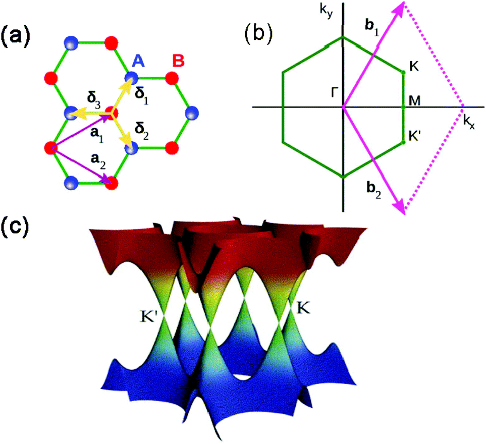 | ||
| Fig. 1 (a) Hexagonal crystal lattice of graphene. a1 and a2 are the lattice unit vectors, and δi, i = 1,2,3 are the nearest-neighbour vectors. (b) Graphene's Brillouin zone. The Dirac cones are located at the K and K′ points. (c) The energy dispersions of graphene crystal lattice. The conductance band touches the valence band at the K and the K′ points (i.e. the Dirac points). (Taken from ref. 69. Open access from Elsevier.) | ||
The most interesting aspect of the graphene energy spectrum is that its charge carriers can be described by a Dirac spectrum for massless fermions73 rather than the usual Schrödinger equation for nonrelativistic particles.5,9 The quasiparticles in graphene exhibit a linear dispersion relation following the equation E = ħkvF, as if they were massless relativistic particles governed by the Dirac equation.5,9 (Here, the role of the speed of light c is replaced by Fermi velocity vF ≈ c/300.) This means that electrons in graphene all move at a constant velocity (∼vF) regardless of their momentum. Because of this linear dispersion, the quasiparticles in graphene behave very differently from other semiconductors or metals, with an energy spectrum approximated by parabolic (i.e. free electron-like) dispersion relations.
For example, although the bandgap is zero, the gate voltage can still modulate the density of states in graphene74 and switch from low conductivity states near the Dirac point to high conductivity states elsewhere (Fig. 2). However, because there is no bandgap, there is still a finite amount of current even at the low conductivity state near the Dirac point,74–76 leading to high switch-off current in graphene-based transistors. The minimum conductivity is also affected by defects, impurities and the chiral nature of electrons in graphene.10,75,76
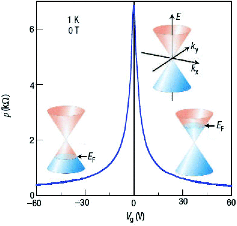 | ||
| Fig. 2 Ambipolar electric field effect in single-layer graphene. The insets show its low-energy spectrum, indicating changes in the position of the Fermi energy EF with varying gate voltage Vg. (Taken from ref. 4. Reproduced with permission from Nature Publishing Group.) | ||
The graphene crystal also shows exceptional electronic qualities such that charge carriers can travel ballistically over a submicron distance.5,9,10,77 Room temperature mobility values exceeding 100![[thin space (1/6-em)]](https://www.rsc.org/images/entities/char_2009.gif) 000 cm2 V−1 s−1 have been reported in the literature.10,78–80 The mobility in these samples is limited by scattering on charged impurities81 or microscopic ripples.9,82 However, both sources of scattering can be reduced significantly by careful sample preparation, and they are not the ultimate limiting factors of carrier mobility in the graphene structure.77 It is the intrinsic scatterer such as the phonon, which cannot be removed at room temperature that sets the fundamental limit of mobility in graphene.10,77
000 cm2 V−1 s−1 have been reported in the literature.10,78–80 The mobility in these samples is limited by scattering on charged impurities81 or microscopic ripples.9,82 However, both sources of scattering can be reduced significantly by careful sample preparation, and they are not the ultimate limiting factors of carrier mobility in the graphene structure.77 It is the intrinsic scatterer such as the phonon, which cannot be removed at room temperature that sets the fundamental limit of mobility in graphene.10,77
Graphene's carrier transfer characteristic also stands out as it shows a perfect ambipolar electric field effect so that its charge carrier can be tuned continuously as shown in Fig. 2.5,9,72 Its low-energy spectra are shown as insets in Fig. 2, indicating the changes in the position of the Fermi energy EF with respect to the gate voltage Vg. Positive gate voltage induces electrons while negative voltage induces holes. With its unique ambipolar transport properties and exceptional carrier mobility, graphene is highly applicable to RF electronics. Hence, some of the earliest studies on graphene electronics were focused on high-speed transistors and unique analog circuitry exploiting ambipolarity.34,38,46,48,59,83
Electronic properties of layered TMDs
One aspect of graphene that severely limits its applicability is the lack of bandgap and the resulting leakage of current during transistor operation.8 Various functionalized forms of graphene can introduce an energy gap but only at the cost of reduced electronic properties, such as degraded mobility.84,85 Several TMDs, on the other hand, are gapped semiconductors65 and still retain the exotic qualities because their thicknesses are comparable to that of graphene (graphene is roughly ∼3 Å86 thick while most monolayer TMDs are ∼7 Å thick2,87). For example, the bandgap of a monolayer MoS2 is found to be around 1.9 eV with a thickness of ∼6.9 Å.2,25
Generally, TMDs have the stoichiometric formula of MX2, where M is a transition metal from group 4 to 10, and X is a chalcogen (S, Se, Te). The crystalline structure consists of transition metal atoms forming hexagonal crystal lattices that reside between chalcogen atom layers. Although most TMDs based on group 4–7 elements are layered (such as MoSe2, WS2, WSe2, HfSe2, NbSe2, TaSe2, NiTe2, etc.), it is worth noting that some TMDs based on group 8–10 elements (such as FeSe2) are not layered materials.7
Fundamentally, all 2D materials are inevitably affected by the interlayer coupling and the quantum confinement.7,66 Layered multilayers exhibit dramatically different electronic properties from 2D monolayers.7,65,66 The band structure of these materials can be calculated from the density functional theory.65,66Fig. 3 depicts the band structure obtained for bulk, quad-, bi-, and mono-layer of an MoS2. With reduced layer thickness, the indirect bandgap becomes larger, while the direct excitonic transition barely changes. The lowest energy transition changes as the black arrow indicates, and this results in an indirect to direct bandgap transition. This, in turn, also results in a larger bandgap for monolayer MoS2. Experimentally, this development is confirmed as enhanced photoluminescence in single-layered MoS2.66 This property is a direct consequence of quantum confinement and can be observed in other 2D TMDs, such as MoSe2, WS2, and WSe2.1,66,83,88,89 Consequently, semiconducting TMD monolayers tend to have larger bandgaps than their bulk counterparts.
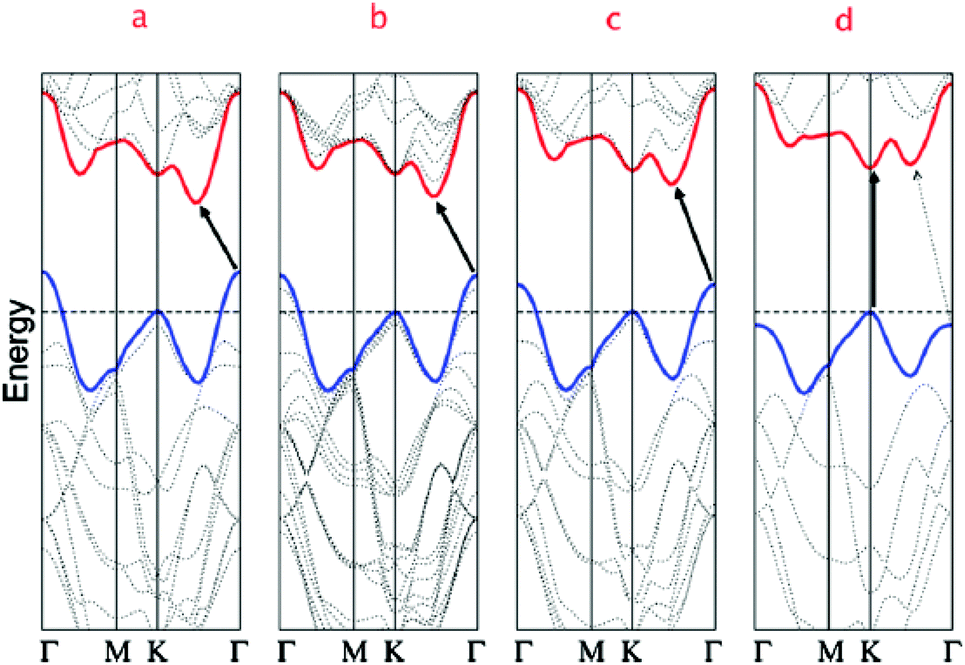 | ||
| Fig. 3 Calculated band structures of (a) bulk MoS2, (b) quadlayer MoS2, (c) bilayer MoS2, and (d) monolayer MoS2. The solid arrows indicate the lowest energy transitions. (Taken from ref. 66. Reproduced with permission from the American Chemical Society.) | ||
Fig. 4 shows the calculated band alignments for several known monolayer TMDs.65 A few notable trends can be observed from the band alignments. As the atomic number of the X (chalcogen) increases, both the valance band maximum and the conduction band minimums increase. Also, the valance band offset tends to be larger than the conduction band offset, leading to smaller bandgaps for TMDs with larger atomic number chalcogens. Moreover, the conduction and valence band of W-based TMDs are higher than those of Mo-based TMDs. The band offsets are generally determined by the repulsion strength from the cation d orbitals and the anion p orbitals.66 The overlap integral of d and p orbitals and the differences in energy as well as the M–X bond length determine the overall band offsets and its alignment.66
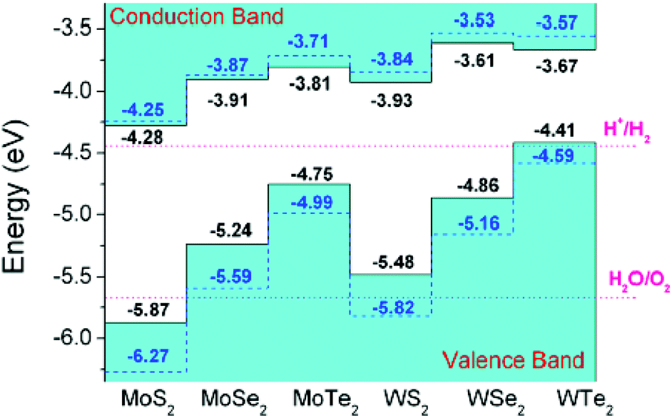 | ||
| Fig. 4 Calculated band alignment for transition metal dichalcogenide monolayers. Solid lines and dashed lines are obtained by different simulation approaches. The dotted lines indicate the water reduction (H+/H2) and oxidation (H2O/O2) potentials. The vacuum level is taken as zero reference. (Taken from ref. 65. Reproduced with permission from the American Institute of Physics.) | ||
An interesting aspect of the 2D material is that some materials (e.g. graphene, WSe2) tend to be p-type while some materials (e.g. MoS2, MoSe2) tend to be n-type in ambient air. Atomically thin p–n junctions have been formed exploiting this trait.91 Furthermore, physisorption of gas adsorbates either depletes or accumulates charges resulting in opposite effects for n-type and p-type 2D materials. For example, physisorbed O2 and H2O molecules deplete n-type MoS2, which weakens the electrostatic screening and leads to the enhancement of photoluminescence.92 In WSe2, the opposite effect was observed.92
Finally, it is worth noting that there are two possible polymorphs of monolayer TMDs (Fig. 5). For a trigonal prismatic (2H) phase, atoms of each chalcogen layer are directly on top of the other chalcogen layers. The trigonal antiprismatic phase (often referred as octahedral or 1T), on the other hand, has alternating chalcogen layers offset from each other as shown in Fig. 5b.90 This difference in the atomic arrangement has a profound effect on the band structure. Progressive filling of the non-bonding d bands of the transition metal atoms leads to either metallic or semiconducting behaviour. For MoS2, the 2H form is semiconducting while the 1T form is metallic.90 The preferred phase of a TMD is mainly determined by the number of d-electrons in the transition metal. For example, group 4 TMDs are mostly trigonal antiprismatic while group 6 TMDs are predominantly trigonal prismatic. Group 5 TMDs are found in both forms.7
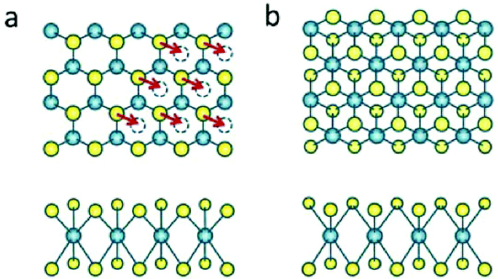 | ||
| Fig. 5 Illustration of the MoS2 structure viewed from the out-of-plane and in-plane axes. The blue and yellow spheres represent Mo and S atoms. (a) 2H phase MoS2. Only the S atoms on the upper planes can be seen from the c-axis as those on the lower planes are directly underneath the top atom. The arrows in panel a show the local S plane glide motion that leads to local transformation to 1T structure. (b) 1T phases. (Taken from ref. 90. Reproduced with permission from the American Chemical Society.) | ||
Graphene-based analog/RF circuits
The lack of bandgap in graphene limits graphene's role in traditional logic applications. However, this requirement of a high on/off ratio is less stringent in analog/RF electronics.8 In a single-stage amplifier, for example, the transistor operates in the on-state while a small signal is superimposed on the DC gate voltage. Furthermore, the charge carriers in graphene exhibit extremely high carrier mobility with zero effective mass.10,77,86 Combined with its unique two dimensional structure, graphene is potentially well suited for high speed RF applications. Transistors with cut-off frequencies as high as 300 GHz were demonstrated with both exfoliated30 and CVD synthesized42 graphenes. Hence, the unique properties of graphene have led to plenty of novel RF components, including mixers,38–40 frequency multipliers,34,36,46 modulators,35,37 and amplifiers.41–43Frequency multipliers
Frequency multiplication has always been an integral part of various analog electronics and communication systems. Most frequency multipliers, however, are realized by generating harmonics from nonlinear components such as diodes and filtering out the necessary signals with additional components.93 The major drawback of this method is the low efficiency (<30%) and the requirement of additional filtering components. With graphene-based transistors, however, it is possible to multiply signals very efficiently with only one transistor by exploiting the ambipolar transport behaviour.34,35As shown in Fig. 6a, positive gate voltage induces electrons with NFET-type response while negative gate voltage induces holes with PFET-type response. The gate voltage that results in minimum conductance is called the Dirac point voltage or the charge neutrality point (CNP) voltage. The Dirac point voltage may drift from 0 V depending on the environmental doping effects.18 Nevertheless, the environmental doping can be controlled with meticulous sample preparation and a capping passivation layer.77
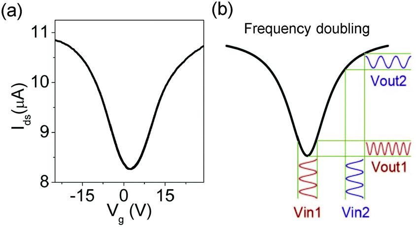 | ||
| Fig. 6 (a) Typical Id–Vg curve of a graphene transistor. (b) Frequency modulation is achieved by interchanging the bias point from a region dominated by electron (or hole) carriers to the charge neutrality point. (Taken from ref. 37. Reproduced by permission of Nature Publishing Group.) | ||
As shown in Fig. 6b, applying an oscillating input signal (Vin2) on either side of the Dirac point voltage will result in an output signal (Vout2) with the same frequency. However, when the input signal (Vin1) is directly applied at the Dirac point voltage, the frequency of the output signal (Vout1) will be twice the original value. This is the result of a sudden change in the phase of the signal when the original input signal crosses the Dirac point.
Several frequency multipliers, including doublers using one transistor (Fig. 7) and a tripler using two transistors (Fig. 8), have been demonstrated. The tripler uses two graphene transistors with different Dirac point voltages to obtain two conduction dips for additional change in the phase. Remarkably, the output signals of these multipliers have very high spectral purity with over 90% of the RF power in the multiplied frequency range.34,46 It is important to note that rather complex circuits with multiple transistors/diodes and other passive components are required to enable frequency multiplication with current CMOS technology.93 The ambipolarity is also the key aspect of modulators and mixers based on graphene transistors.
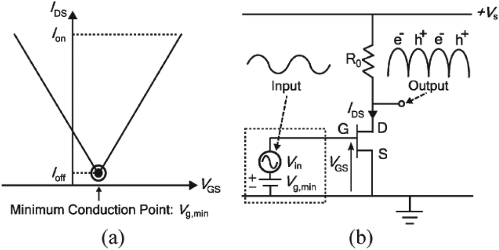 | ||
| Fig. 7 (a) Linear approximation of the transfer characteristic of ambipolar graphene FETs. The minimum conduction point is equal to the quiescent bias point for full-wave rectification and frequency doubling. (b) With the device being biased at the minimum conduction point, electrons and holes conduct alternatively in half-cycles of the output signal. (Taken from ref. 34. Reproduced with permission from the Institute of Electrical and Electronics Engineers (IEEE).) | ||
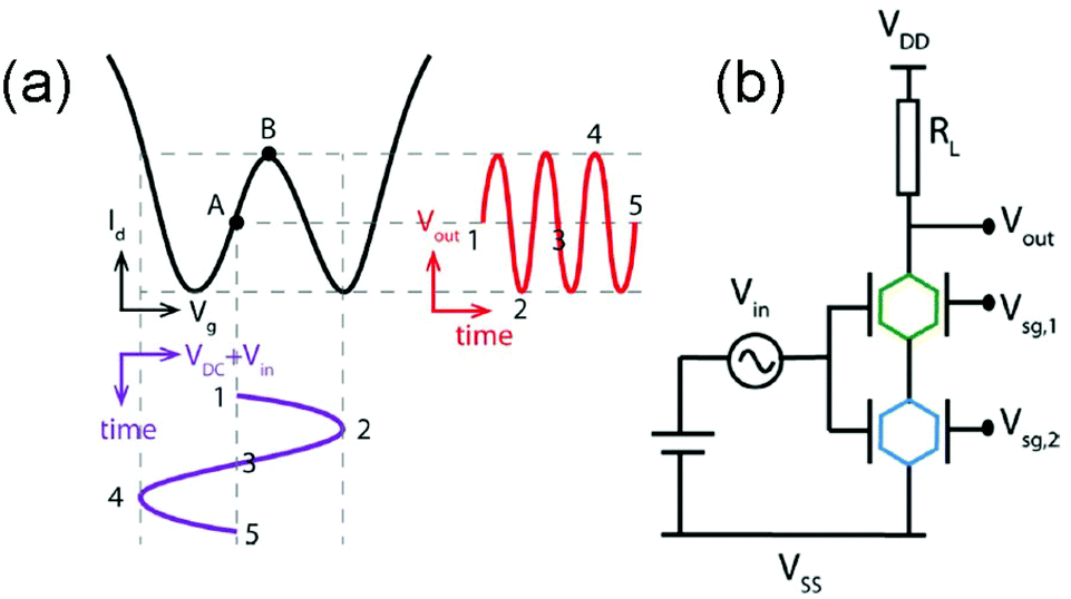 | ||
| Fig. 8 (a) Schematic diagram illustrating the operation principle of a graphene frequency tripler. The input waveform and output waveform are shown in purple and red respectively. The input dc voltage bias (point A) is chosen halfway between the voltages where minimum current occurs and the central current peak (point B). Points in time 1 through 5 in the input cycle correspond to those labelled in the output waveform. (b) Circuit schematic of the graphene frequency tripler. Vsg1 and Vsg2 are dc voltages used to control the threshold voltage separation electrostatically between two graphene FETs. (Taken from ref. 46. Reproduced with permission from the American Chemical Society.) | ||
Modulators
In today's communication systems, modulation is an essential function that embeds the baseband signal (information) into a carrier wave so that it can be successfully broadcasted through a medium such as air. The basic modulation techniques map the information by varying up to three different parameters (amplitude, frequency and phase) of the carrier wave to represent the data. The most fundamental modulation techniques that correspond to each of these three parameters are amplitude modulation (AM), frequency modulation (FM), and phase modulation (PM).94Similar to frequency multiplication as explained in the previous section, the unique ambipolar gate response of graphene transistors allows simple implementation of the three basic modulation schemes as illustrated in Fig. 9. The amplitude, frequency, and phase of the output voltage are determined by the operating gate bias point of the graphene transistor. For example, amplitude modulation (AM) can be achieved by utilizing the transconductance change over the gate voltage difference. Frequency modulation (FM) is achieved by interchanging the bias point from a region dominated by electron (or hole) carriers to the charge neutrality point. Similarly, phase modulation (PM) is realized by changing the bias point from a region dominated by an electron (or hole) carrier to a region dominated by the hole (or electron) carrier. The most basic modulation schemes that encode 1 bit of data (i.e. 0 or 1) per signal are called binary modulation schemes. Several pioneering studies have been done to verify the fully functioning binary modulators.35,95
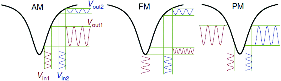 | ||
| Fig. 9 Illustrations of amplitude, frequency and phase modulation of a sinusoidal wave achieved by operating a single ambipolar graphene transistor at different gate biases. (Taken from ref. 37. Reproduced with permission from Nature Publishing Group.) | ||
By combining two or more of these binary modulation schemes, it is possible to extend this technique into quaternary modulation schemes such as quadrature phase-shift keying (QPSK).37 Specifically, QPSK is the key building unit for highly efficient modulation techniques that are widely used in today's telecommunication standards.
Fig. 10a shows a typical QPSK transmitter structure used in modern digital communication. A binary data stream is demultiplexed into the in-phase component (I) and the quadrature-phase component (Q). I and Q components are encoded onto two orthogonal basis functions, such as a sine wave and a cosine wave, respectively, before they are summed to generate a QPSK modulated signal.
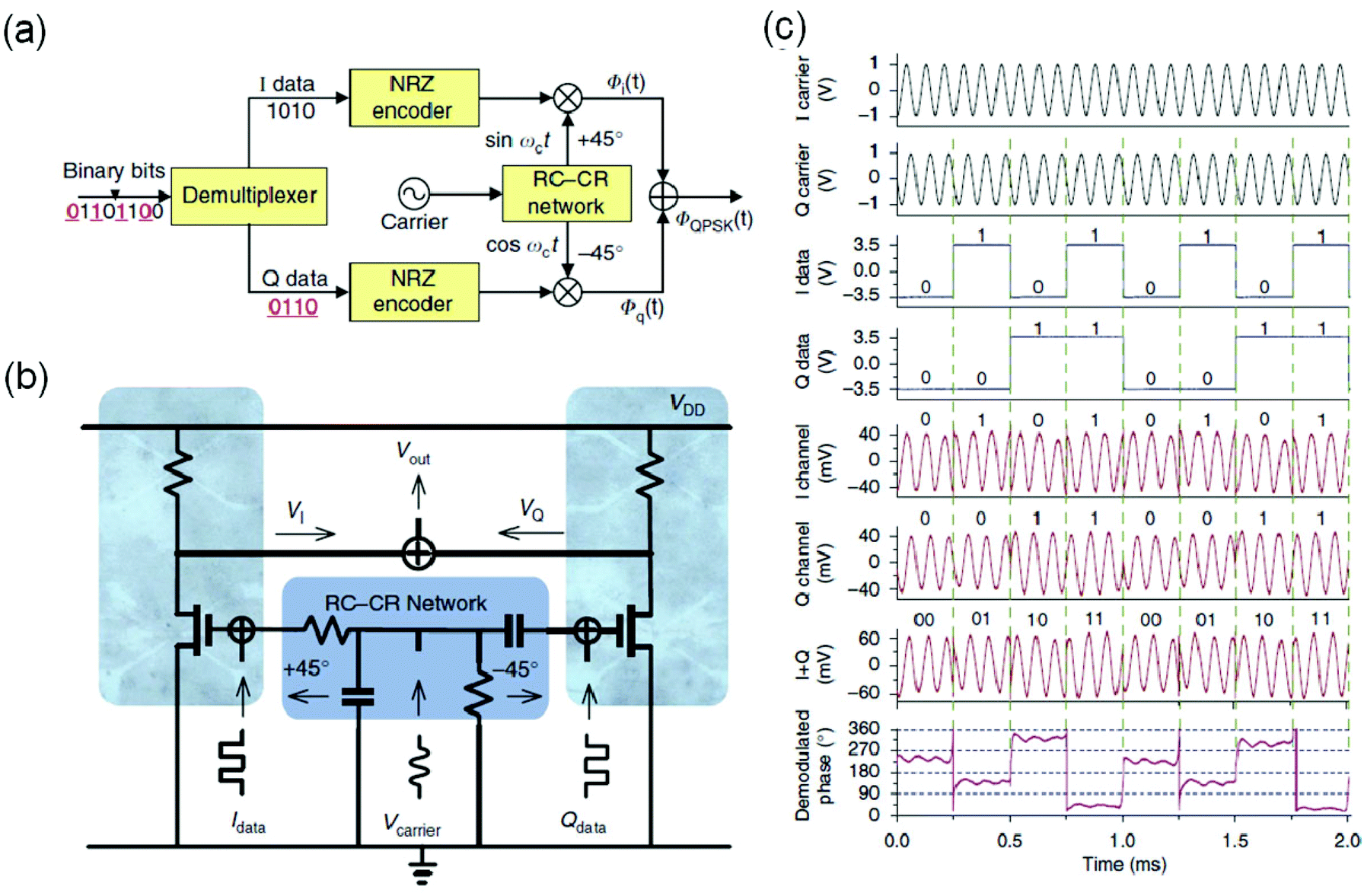 | ||
| Fig. 10 QPSK demonstrated with two all-graphene transistors. (a) A conceptual diagram of a conventional QPSK transmitter structure. The NRZ encoder is a non-return-to-zero encoder, where 1 is represented by a positive voltage state and 0 is represented by a negative voltage state. The RC–CR network is the resistance-capacitance–capacitance-resistance phase shift network that generates two orthogonal wave functions with 90° phase difference. (b) An all-graphene circuit diagram of the QPSK system using two transistors. The actual microscopic image of the all-graphene circuit under a blue filter is shown. (c) Time domain plots of the input and output signals demonstrating QPSK modulation scheme. (Taken from ref. 37. Reproduced with permission from Nature Publishing Group.) | ||
In this work, two transistors are used to demonstrate the QPSK modulation (Fig. 10b). Actual microscope images under a blue filter were overlaid on top of the circuit diagram. A sinusoidal wave from the function generator was connected to a simple off-chip resistance-capacitance–capacitance-resistance (RC–CR) phase shift network to generate two orthogonal wave functions with 90° phase difference. The sinusoidal input is shifted by +45° in the CR branch and by −45° in the RC branch. Then each of these signals is summed internally by the function generators with two square waves (Idata and Qdata) and fed to the gates of each transistor. The outputs (VI and VQ) are then summed to generate the final QPSK modulated signals. These signal components are plotted in Fig. 10c. The Icarrier and the Qcarrier are the orthogonal carrier signals. The data bitstream with 00, 01, 10, 11 is represented by the in-phase component Idata and the quadrature-phase component Qdata as shown in the plot. Modulating Icarrier with Idata results in phase changes in Ichannel and the same applies to Qcarrier, Qdata, and Qchannel. Data bit 0 and 1 in Idata correspond to phase of 180° and 0° in Ichannel. Similarly, Data bit 0 and 1 of Qdata correspond to phase of 90° and 270° in Qchannel. The sum of Ichannel and Qchannel is the final output signal (I + Q), which has distinct phase shifts of 225°, 135°, 315°, and 45°, each corresponding to binary data of 00, 01, 10, and 11, respectively. To validate the result, the instantaneous phase information was extracted from the final output signal (I + Q) and plotted as a demodulated phase (Fig. 10c, bottom panel).
Mixers
Another inevitable consequence of ambipolarity is an acute nonlinearity in the vicinity of the Dirac voltage. The transfer characteristics of an ambipolar graphene FET are symmetrical around the Dirac voltage. This symmetrical characteristic usually results in a very significant quadratic component, and therefore mixers based on this characteristic can effectively suppress odd order intermodulation and lead to lower spurious emissions in the circuit.38 A mixer based on graphene was demonstrated at a frequency of 10 MHz using graphene grown by chemical vapour deposition, and a high-quality factor was observed with a third-order intercept point of +13.8 dBm.38A high-performance mixer fabricated by integrating graphene transistors and passive components on a single silicon carbide wafer (Fig. 11) was also developed.39 The importance of this work is twofold: demonstration of multi-level, wafer-scale integration, and verification of superior thermal stability in graphene-based transistors compared to conventional ones. The absence of strong temperature dependence in graphene is attributed to a degenerate doping level in graphene and a nearly temperature-independent scattering mechanism associated with optical phonons at high biases.39 The mixer operated at frequencies up to 10 gigahertz and exhibited exceptional thermal stability with little reduction in performance up to 400 kelvin.
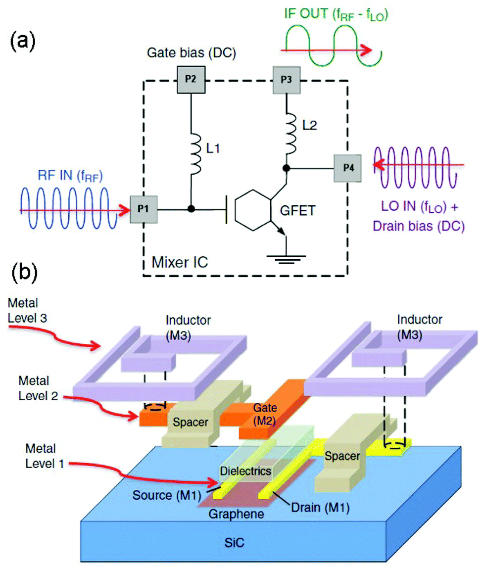 | ||
| Fig. 11 (a) Circuit diagram of a graphene RF frequency mixer on a SiC wafer. (b) Illustration of a graphene mixer circuit. The design components include a graphene transistor and two inductors connected to the gate and the drain of the GFET. Three distinct metal layers of the graphene IC are represented by M1, M2, and M3. (Taken from ref. 39. Reproduced with permission from the American Association for the Advancement of Science.) | ||
In contrast to the previous two studies on fundamental mixers, a subharmonic graphene FET mixer (Fig. 12) was recently demonstrated.40 A subharmonic mixer needs only half the local oscillator (LO) frequency of a fundamental mixer. In addition, subharmonic mixers suppress the LO noise, and the wide frequency gap between the RF and LO signals simplifies the LO and RF separation. Also, a balun is not required, as opposed to conventional subharmonic resistive FET mixers, which require two FETs in parallel and a balun for feeding the two out-of-phase LO signals.40 The circuit topology is shown in Fig. 12. Modulating the gate voltage results in a time-varying channel resistance Rds(t). Due to the biasing at the Dirac point, Rds(t) varies as a function of 2 × fLO (frequency doubling). The time-varying reflection coefficient is Γ(t) = (Rds(t) − Zo)/(Rds(t) + Zo) seen in the drain of the graphene FET, where Zo = 50 Ω is the system impedance. By feeding an RF signal VRF+(t) to Γ(t), the reflected signal (i.e. output voltage) V−(t) = Γ(t)VRF+(t) is generated. The reflected voltage has frequency components at |fRF ± 2nfLO|, and the IF component (fIF = |fRF − 2fLO|) is the desired one for the down-conversion mixer. A down-conversion loss of 24 dB was obtained with fRF = 2 GHz, fLO = 1.01 GHz, and fIF = 20 MHz.
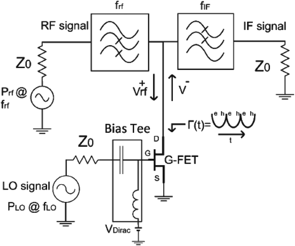 | ||
| Fig. 12 Circuit structure of the subharmonic resistive graphene FET-based mixer. (Taken from ref. 40. Reproduced with permission from the Institute of Electrical and Electronics Engineers (IEEE).) | ||
Amplifiers
Before we continue on to amplifiers, different terms related to different gains have to be clarified. In this paper, ƒT ≈ gm/2πCox denotes the cut-off frequency, defined as the frequency at which the current gain becomes unity (gm is the transconductance and Cox is the gate capacitance). ƒT is obtained from the short-circuit current gain h21, while the load impedance is nonzero. ƒmax is related to the power gain obtained assuming the best impedance matching. It is the highest possible operating frequency before a transistor loses its ability to amplify power. Open-circuit voltage gain refers to the condition of infinitely high load impedance. The open-circuit voltage gain is related to the intrinsic gain Gint, obtained from the ratio gm/gd, where gm is the transconductance and gd is the output conductance.It is very important to distinguish these figures of merit for graphene transistors because of graphene's weak saturation behaviour.8 High ƒT numbers reported for graphene transistors can be misleading. This ƒT results directly from graphene's high mobility.8 However, since the drain current does not saturate in these devices, they exhibit limited power gain and voltage gain than what is required for practical RF circuit applications.8,42,43
Hence, several studies were focused on obtaining sizeable voltage gain in graphene transistors.41–43 Han et al. partially solved the drain current saturation problem in graphene FET with an extremely thin and planar gate dielectric.43 They have exploited the fact that the shift of the Dirac point with good gate control should be equal to half of the applied drain bias.49 This shifting of the Dirac point translates into a clear drain current saturation. However, graphene is a highly inert material and techniques such as atomic layer deposition are not ideal methods to form a pinhole-free dielectric. Hence, they used a chemical–mechanical polishing (CMP) method to form a very flat and thin bottom gate dielectric (HfO2, 4 nm thick) underneath the graphene layer. The graphene common-source amplifier fabricated with this method exhibited 5 dB low frequency gain with the 3 dB bandwidth greater than 6 GHz.43
There are other studies that also exploited the Dirac voltage shifting effect.41 In Fig. 13, a voltage amplifier was realized with a complementary push–pull configuration. By applying the supply voltage VDD, the potential of the graphene channel in G2 increases with respect to that of G1, which therefore shifts the Dirac point of G2 to higher input voltages. Complementary operation is obtained between the Dirac points of the two FETs, where the increase in input voltage VIN causes the resistance of G2 to increase and the resistance of G1 to decrease. This results in a large rate of increase for the output voltage VOUT as the input voltage VIN changes, and doubles the voltage gain Av compared to a single graphene FET-based common-source amplifier. The amplifier had a voltage gain of 3.7 (11.4 dB) at 10 kHz, a total harmonic distortion in the audio frequency range of <1%, a unity-gain frequency of 360 kHz and a −3 dB bandwidth of 70 kHz.41
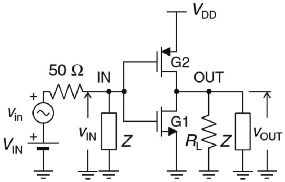 | ||
| Fig. 13 A circuit diagram of the graphene transistor-based amplifier with complementary push–pull configuration. Z = 1 MΩ is the input impedance of the oscilloscope while 50 Ω is the output resistance of the input voltage source. VIN is the DC bias voltage and vin(t) is the AC component of the input signal. The amplifier is additionally loaded with RL to simulate the next amplifying stage. (Taken from ref. 41. Reproduced with permission form Wiley.) | ||
Subsequently, state-of-the-art graphene FET-based amplifiers with intrinsic cut-off frequencies above 300 GHz were also developed.42 This work was done in wafer-scale with both CVD-synthesized and epitaxially grown graphene, and the value of ƒT is the current record for graphene-based RF electronics. These devices also exhibited voltage and power gains reaching 20 dB. This was achieved by minimizing the scattering effect at the interfaces with ultra-smooth, diamond-like carbon substrates.29 The channel doping was also minimized to greatly improve the transconductance and current saturation. Fig. 14a and b show interesting results from these devices. ƒT for both CVD graphene and epitaxial graphene exhibits the typical 1/L trend (Fig. 14a). There is very little performance gap between CVD graphene and epitaxial graphene. ƒmax, on the other hand, reaches a peak value at around 200 nm channel length (Fig. 14b). This peak in ƒmax is the result of competing contributions from ƒT, gate resistance, and output conductance gd as the gate length decreases.94,95 Since the ƒmax value does not represent the intrinsic performance, but is affected by extrinsic components, the power gain can be improved by better saturation behaviour and the optimization of parasitic components.
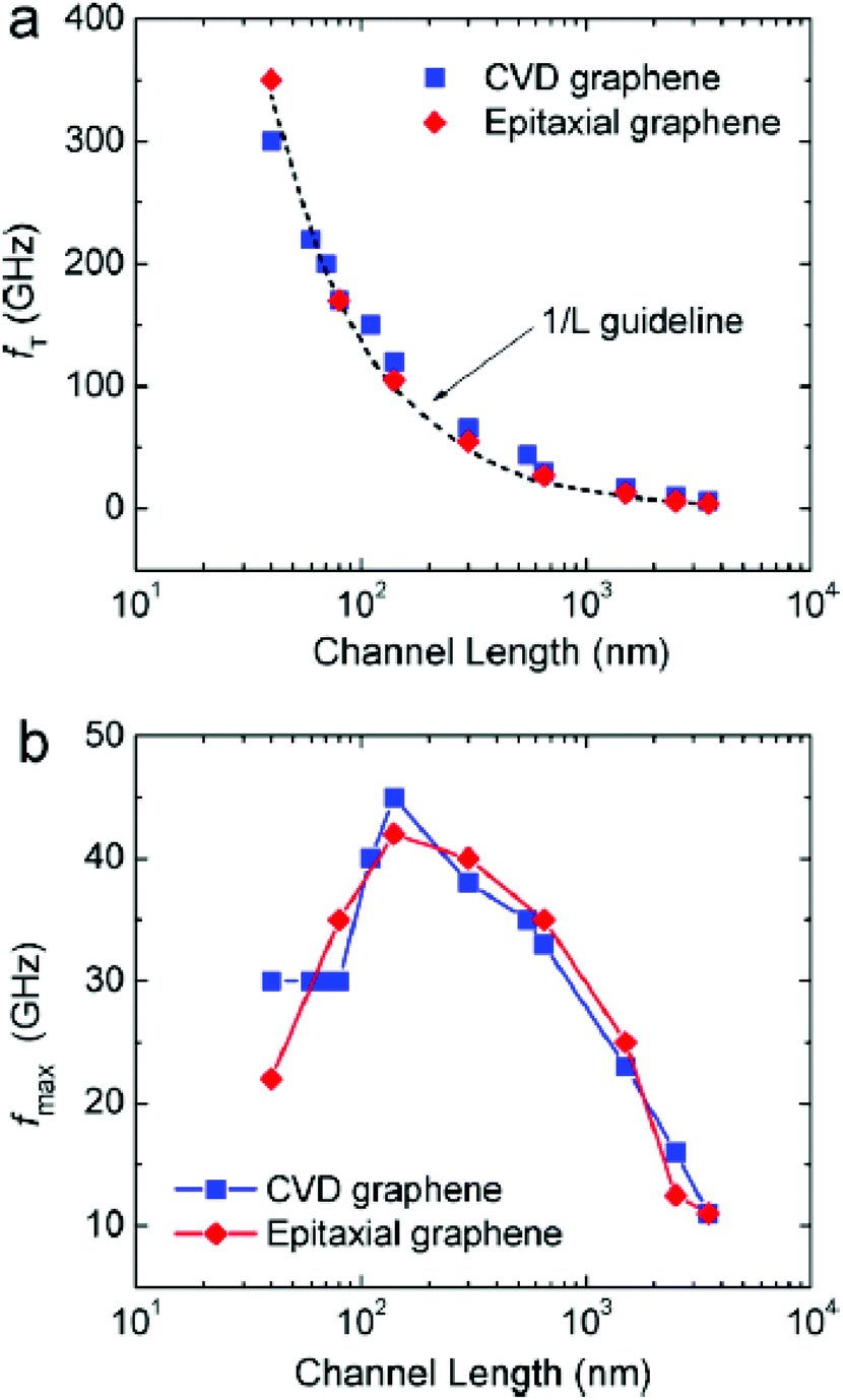 | ||
| Fig. 14 (a) Scaling behaviour of ƒTversus channel length, showing the clear 1/L dependence. (b) ƒmaxversus channel length with the peak ƒmax obtained at a channel length of 140 nm. (Taken from ref. 42. Reproduced with permission from the American Chemical Society.) | ||
CMOS/graphene integrated
Since the discovery of graphene, defining its role in the current CMOS-dominated semiconductor industry was the main goal of many researchers. Due to its unique advantages and the ease of transfer, many believe it will have several key applications tightly integrated with CMOS technology.44,47,96 As shown previously, several RF electronic components have been integrated in wafer-scale circuitry. With significant improvement in fabrication technology, graphene components can now be integrated into circuitry with higher complexity and system functionality. A multi-stage graphene RF receiver integrated circuit is shown (Fig. 15).44 One significant improvement in this work is the preservation of graphene quality during fabrication by applying a passive-first, active-last integration scheme (Fig. 15a). This way, graphene FETs are not exposed during the downstream back-end-of-line (BEOL) process, hence, preventing the degradation of the graphene quality. The entire fabrication flow does not require process steps higher than 400 °C.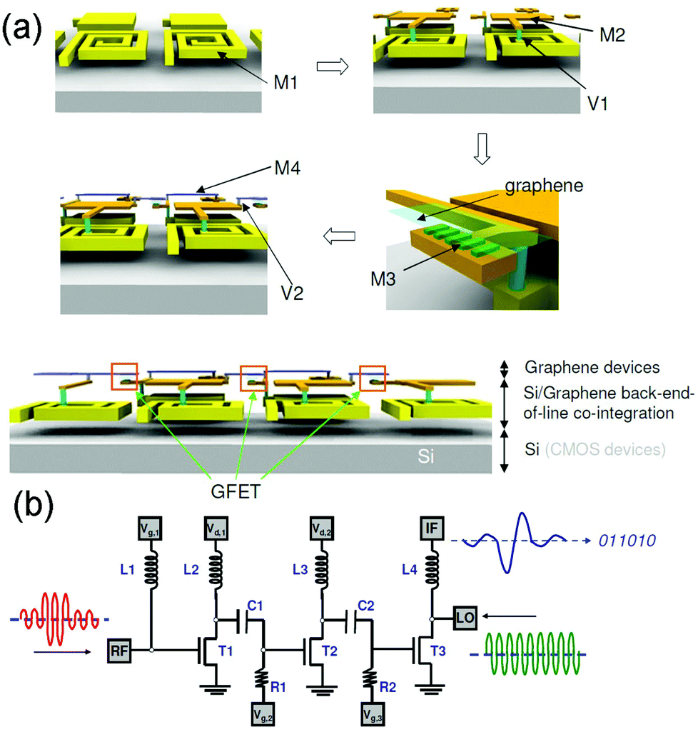 | ||
| Fig. 15 (a) Schematic of the passive-first active-last process flow showing integrated IC fabrication with standard Si BEOL process. Four metal levels (M1–M4) were required. (b) Circuit schematic of graphene RF receiver. Inductor L4, connected at the drain of mixing graphene FET, serves two purposes: it resonates the drain capacitance of transistor T3 to provide a large LO voltage swing at the drain terminal, and also attenuates the LO signal leakage toward the IF port. (Taken from ref. 44. Reproduced with permission from Nature Publishing Group.) | ||
The circuit operates as an RF receiver with front-end performing signal amplification, filtering, and down conversion mixing. All the components are fully integrated into a 0.6 mm2 area and fabricated in 200 mm Si fab, showing complete silicon CMOS process compatibility. The first two stages are designed as bandpass amplifiers, and the third stage performs mixing with the local oscillator (LO) signal which down-converts the GHz RF signal to intermediate frequency (IF) in the MHz range (Fig. 15b). A fundamental drain-pumped mixer design is employed since it leads to better performance based on the characteristics of graphene-based FETs, and results in low LO power requirements (<0 dBm). In Fig. 15b, inductor L4 serves two purposes: It resonates the drain capacitance of transistor T3 to provide a large LO voltage swing at the drain terminal, and also attenuates the LO signal leakage toward the IF port.
To demonstrate the functionality of the graphene IC, an RF carrier of 4.3 GHz was amplitude-modulated with a bitstream and sent to the receiver (Fig. 16). Measured single-bit waveforms in Fig. 16a show IF output signals from the receiver. In Fig. 16b, the bitstream composed of ASCII code modulated at 20 Mb s−1 was received and demodulated. The original bitstream comprising 3 letters (24 bits) was recovered by the graphene receiver with low distortion.
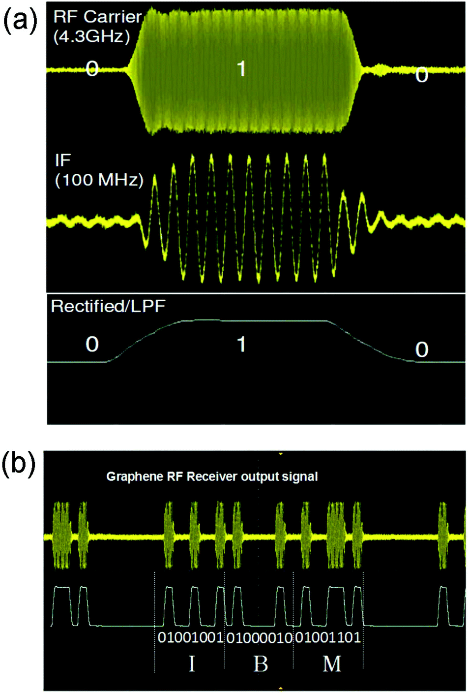 | ||
| Fig. 16 (a) Measured waveforms of RF input signal amplitude modulated at a rate of 20 Mb s−1 (top), IF output signal (middle), and the restored binary code after rectifying and low-pass filtering IF signal (bottom). (b) A screenshot of receiver output waveforms taken from the oscilloscope, with LO power of −2 dBm at 4.2 GHz. (Taken from ref. 44. Reproduced with permission from Nature Publishing Group.) | ||
Graphene-based digital circuits
Even with the inherent lack of bandgap, there were several efforts utilizing graphene in digital electronics by exploiting graphene's unique properties.Inverters
Pioneering work on graphene-based inverters was achieved by fabricating complementary-like logic inverters based on graphene field-effect transistors (Fig. 17a).49 The complementary p- and n-type FET pairs were fulfilled through superposition of Dirac voltage from the applied drain bias. Previously introduced amplifiers also exploited this characteristic.41,43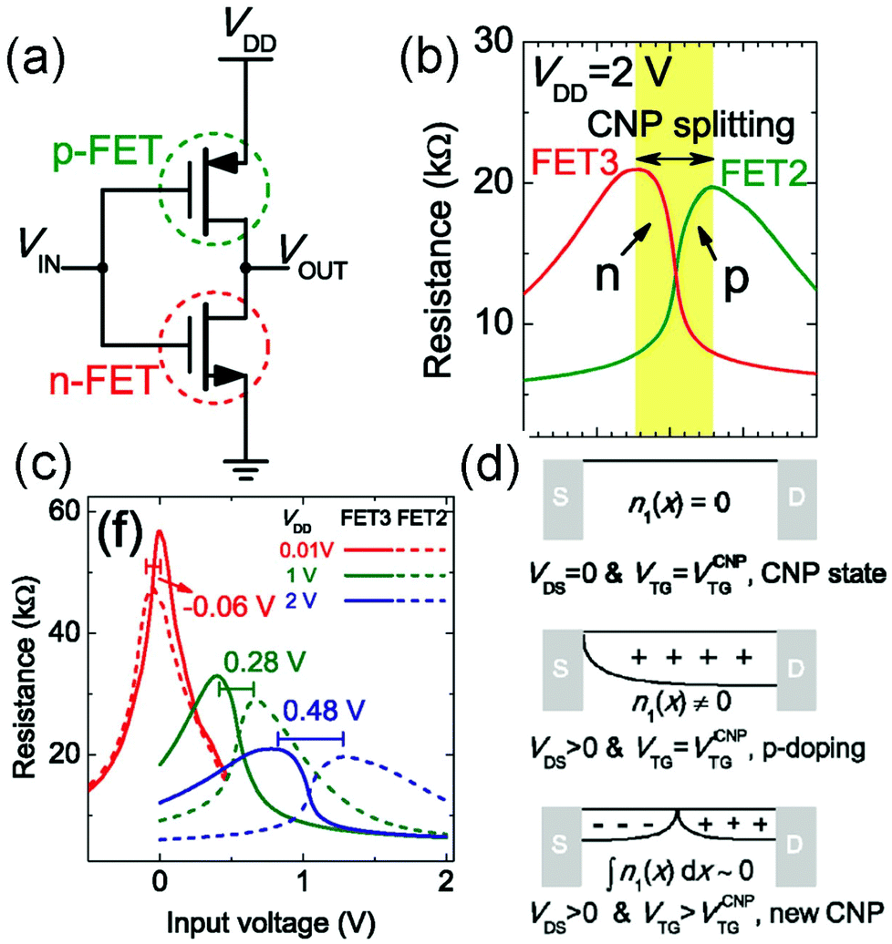 | ||
| Fig. 17 (a) Schematic diagram for the complementary-like graphene inverter. (b) The operating principle for the inverter consisted of FET2 and FET3. Once a CNP splitting between the FET pair is created by high VDD along the input voltage axis, voltage inversion can be achieved in the region of CNP splitting. (c) The resistance behaviour of two FETs (in the inverter) under different VDD. (d) The charge distributions of the FET channel under varied VDS and VTG conditions. (Taken from ref. 49. Reproduced with permission from the American Chemical Society.) | ||
Fig. 17a shows the schematic diagram for the complementary-like graphene inverters. Fig. 17b depicts splitting of the Dirac point or charge neutrality point, due to the effect of VDD. A more detailed explanation is shown in Fig. 17c and d. When positive VDD biases are applied, resistance curves of both FETs shift positively along the VIN axis, in response to the additional superposition potential. Notably, the shift of FET2 is always larger than that of FET3, since FET2 is located upstream in the inverter loop and is affected by higher potential from VDD. By utilizing such an asymmetric shift, the CNP splitting can be controlled electrically (Fig. 17c). In Fig. 17d, when VDS increases, the potential of the channel increases and the effective potential difference between TG and the channel decreases. As a result, the channel deviates from the neutrality condition, and additional positive charges are induced. To introduce charges with opposite polarity and reneutralize the channel, the VTG should increase by roughly half the value of VDS, resulting in a positive shift of IDS minimum along the VTG axis. The inverters achieved voltage gains up to 7, indicating the potential for direct cascading of multiple devices.
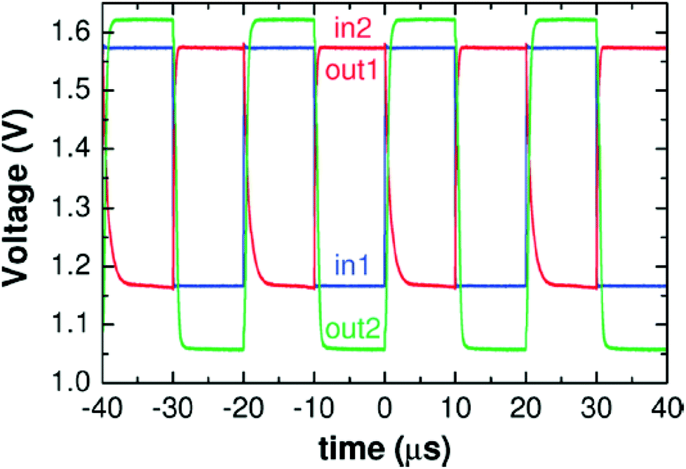
Afterwards, the cascading of these inverters with appreciable voltage gain was successfully demonstrated by another group.50 The cascaded inverters resulted in full-channel gating with a low-frequency voltage gain of Av ∼ 5. Such gain enabled logic inverters with the same voltage swing of 0.56 V at their input and output (Fig. 18).
 | ||
| Fig. 18 Digital waveforms measured under ambient conditions in a cascade connection of two graphene inverters. (Taken from ref. 50. Reproduced with permission from the American Chemical Society.) | ||
Fig. 18 illustrates the digital waveforms measured under ambient conditions in a cascade connection of two graphene inverters. The supply voltage is 2.5 V and the frequency is 50 kHz.
Passive components
Another area of interest for graphene is its applications for passive components. Graphene is not only the strongest and the stiffest material in terms of tensile strength and elastic modulus, respectively; it is also extremely flexible, transparent, and conductive. The close-knit hexagonal crystal structure can also function as an effective barrier against most materials. These exceptional qualities are manifested due to graphene's covalent sp2 bonds. By combining its mechanical strength with unique electrical properties, graphene can be utilized to improve conventional electronic circuits47,53 or provide unique opportunities in niche areas, such as transparent, flexible electronics,37,52 displays, wearable electronics97 and biomedical skin-like devices.98Interconnects
As dimension scaling continues in electronic circuits, many problems such as high resistance and reduced reliability plague copper-based interconnects.53,96 Although interconnects based on carbon nanotubes (CNTs) were also investigated for vertical vias,99 graphene has its advantages because it is compatible with conventional patterning and etching techniques.Many researchers have investigated the application of graphene interconnects for several reasons. First, graphene is several times more conductive than copper of the same thickness.6 It is also known to sustain the highest amount of current density compared to any other known material.6 In addition, it is inherently immune to electromigration,47,96 and it is known to withstand very high temperatures.6 Lastly, graphene is known for its quenching effect of electrical resistance at high temperature. It was found that as the temperature increases from 300 to 500 K, the resistance of single- and bilayer graphene interconnects drops by 30% and 70%, respectively.51 The quenching and temperature dependence of the resistance were explained by the thermal generation of the electron–hole pairs and carrier scattering by acoustic phonons.51
With these inherent advantages, high-speed, on-chip graphene interconnects that operate at frequencies up to 1.3 GHz were integrated with 0.25 μm technology CMOS ring oscillator.47 In the circuit diagram (Fig. 19a), the line is terminated by a termination resistor RT = 20 kΩ to a mid-supply voltage VDD/2. Here the R ∼ 0.5RT is a value determined by the trade-off between the speed improvement provided by the low-swing signalling, and the sensitivity of the differential amplifier at the receiving end. Hence, the signal swing at the receiver end reduced to VDD × R/RT, whereas the speed increased by a factor of R/RT.
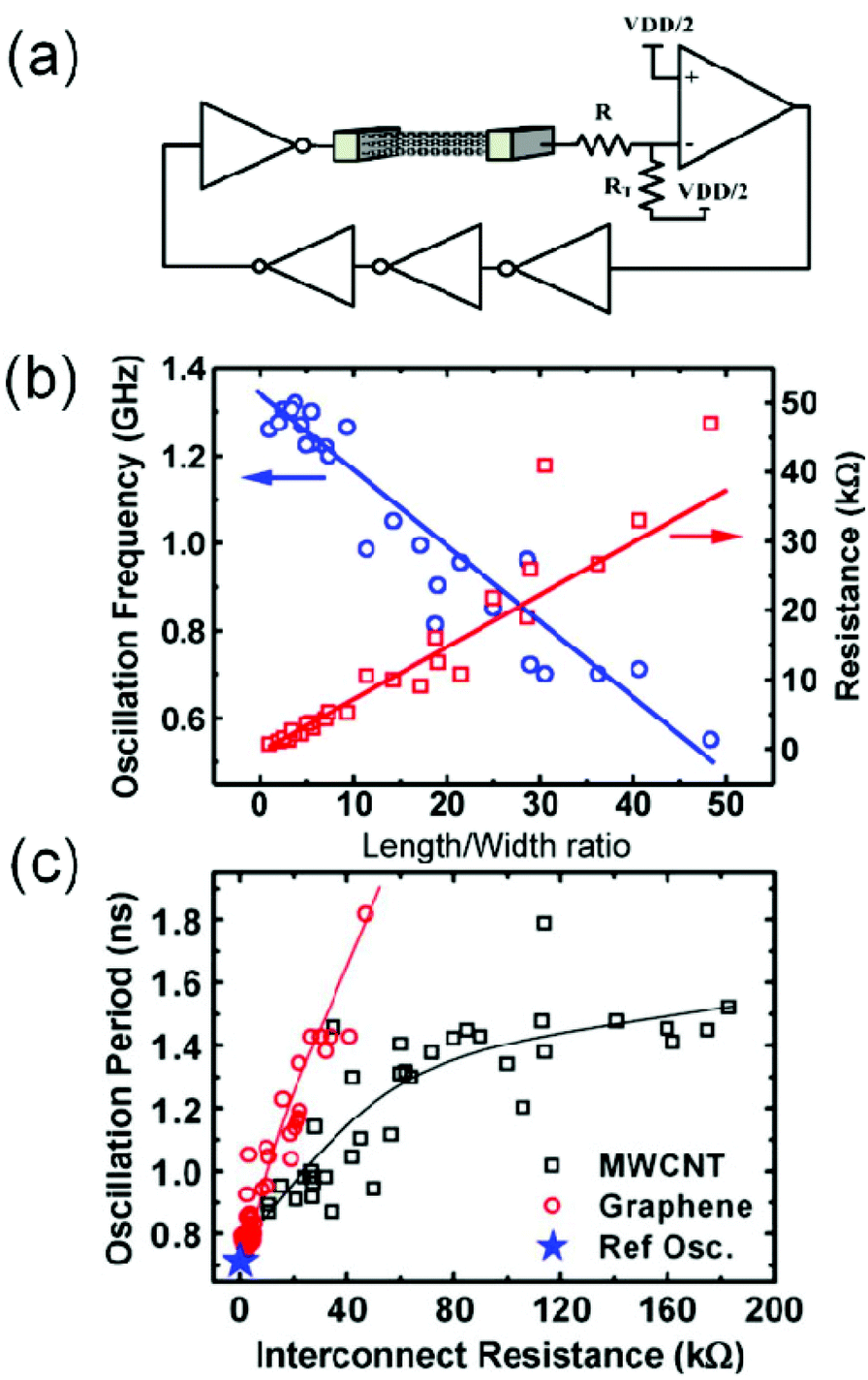 | ||
| Fig. 19 (a) Circuit diagram of a five-stage ring oscillator with a differential amplifier at the receiver end of the inverter chain. (b) Oscillation frequency and resistance as functions of L/W ratio. Symbols represent experimental data and bold lines are visual guides. (c) Oscillation period as a function of interconnect resistance for the CMOS reference interconnects (aluminium), MWCNTs, and graphene. Symbols represent experimental data and bold lines are visual guides. (Taken from ref. 47. Reproduced by permission of the Institute of Electrical and Electronics Engineers (IEEE).) | ||
The circuit oscillation frequency is directly correlated with the interconnect width and inversely correlated with the length/width ratio (Fig. 19b). Oscillation periods as a function of interconnect resistance for the reference interconnects (aluminium), MWCNTs, and graphene are shown in Fig. 19c. Graphene offers a higher oscillation frequency because of its lower resistivity. However, at the same resistance value, the MWCNT has superior signal delay performance. This is due to the larger total capacitance associated with wider graphene strips.
Although the demonstration of graphene interconnects at such high frequency is encouraging, practical problems still remain due to the high growth temperature (∼1000 °C) of graphene.96 The high temperature is a concern since the graphene transfer process is not suitable for massive-scale fabrication of more than ten-level interconnects. A lower temperature process (∼400 °C) with direct deposition capability will be crucial to realize graphene-based interconnects.96
Transparent conductors
Graphene also shows interesting optical properties. Graphene absorbs a significant amount of light per layer (2.3% per layer from ultraviolet to near infrared11). However, because it is only one atomic layer thick, graphene is highly transparent with transmittance of 97.7%. In addition, graphene is also highly conductive due to its semi-metallic properties.4,53 The sheet resistance of a pristine layer is about 2 kΩ to 6 kΩ52,100 and can be as low as 125 Ω with chemical doping.101 The sheet resistance value can be lowered even more by either stacking several graphene layers52 or fabricating a hybrid nanowire/nanomesh structure102 with graphene. Several research groups have demonstrated graphene layers as a transparent conductive material that can compete with some of the oxide-based transparent conductive materials (e.g. indium tin oxide or ITO) that dominate the current market.103 ITO, however, suffers from high cost, material deterioration from ion diffusion, and brittleness, making it incompatible with flexible substrates. Graphene, on the other hand, shows great promise as a transparent conductor due to its high chemical resistivity, low manufacturing cost, and atomically thin, flexible structure.103,104
Fig. 20 shows the sheet resistance of bilayer graphene (BLG) stacks compared with indium oxide under a mechanical deformation. The BLG films were transferred onto polyethylene terephthalate (PET) flexible substrates and patterned for four-probe measurement (Fig. 20a). Two samples of both BLG 1-transfer and BLG 4-transfer were tested in comparison with a commercial indium oxide on a PET substrate under bending conditions. Fig. 20b shows the relative change in sheet resistance versus strain due to bending. At 2.14% strain, the sheet resistance of the indium oxide sample increased by 321% while in the graphene samples it increased only by 10–15%. The indium oxide sample shows a drastic change in sheet resistance due to its brittle nature while graphene samples are much more robust against mechanical stress.
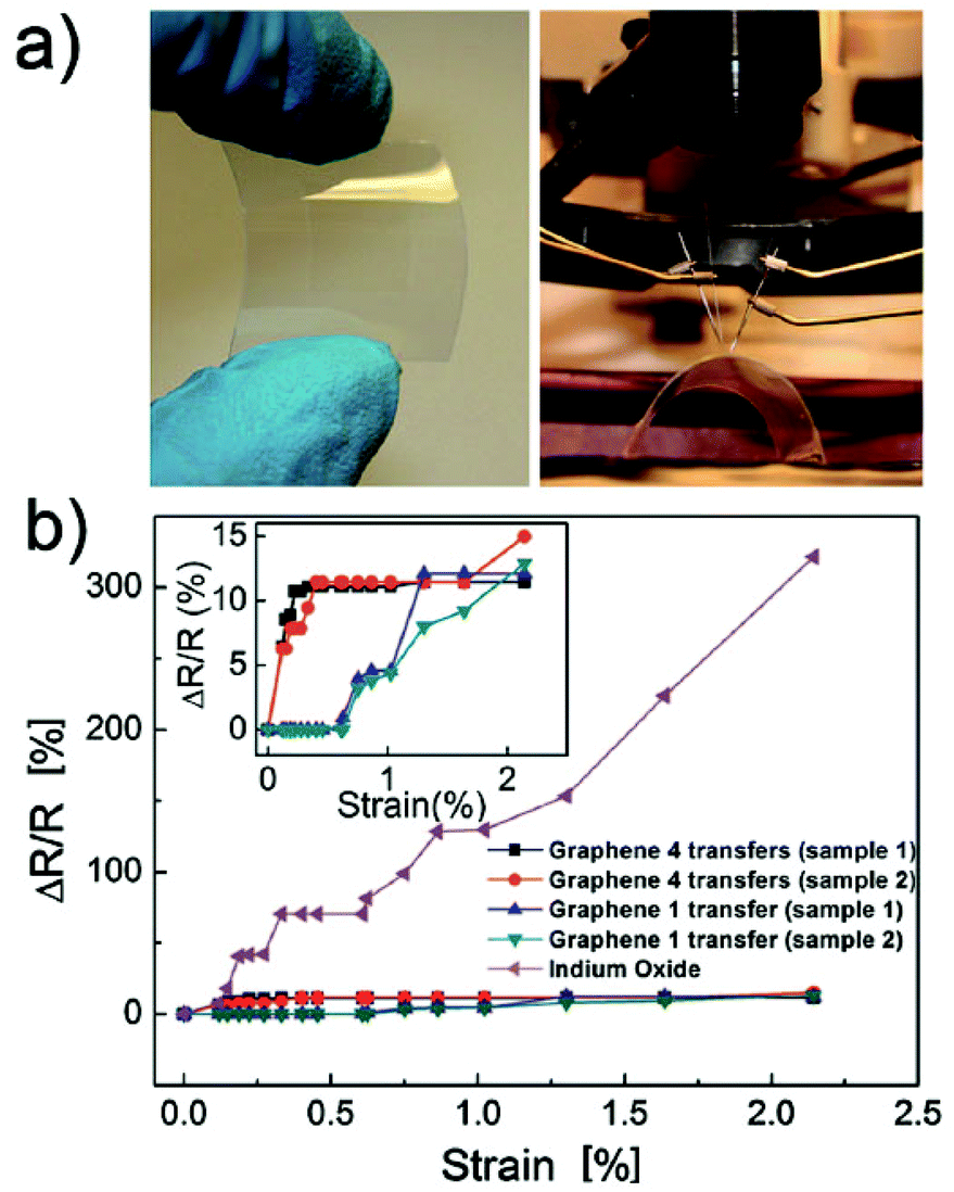 | ||
| Fig. 20 (a) Photographs of a graphene film on the flexed PET substrate (left) and the measurement setup of strained substrates (right). (b) Variation in resistance of stacked BLG films and indium oxide films on 200 mm thick PET substrates as a function of strain values. (Taken from ref. 52. Reproduced by permission of The Royal Society of Chemistry.) | ||
Inductors
Since graphene-based field-effect transistors have already shown potential for analog/RF devices and interconnects, graphene can also be used to design low-loss on-chip inductors that are critical for RF circuits. For designing carbon-based inductors, graphene has a unique advantage over CNTs since it is more controllable from the fabrication point of view.47,53,96 This is due to the planar nature of graphene, which can be patterned using high-resolution lithography (Fig. 21a). Moreover, CNT-based inductors require metal contacts at each corner to connect CNT bundles (Fig. 21b), whereas no such contacts are needed for graphene-based inductors.53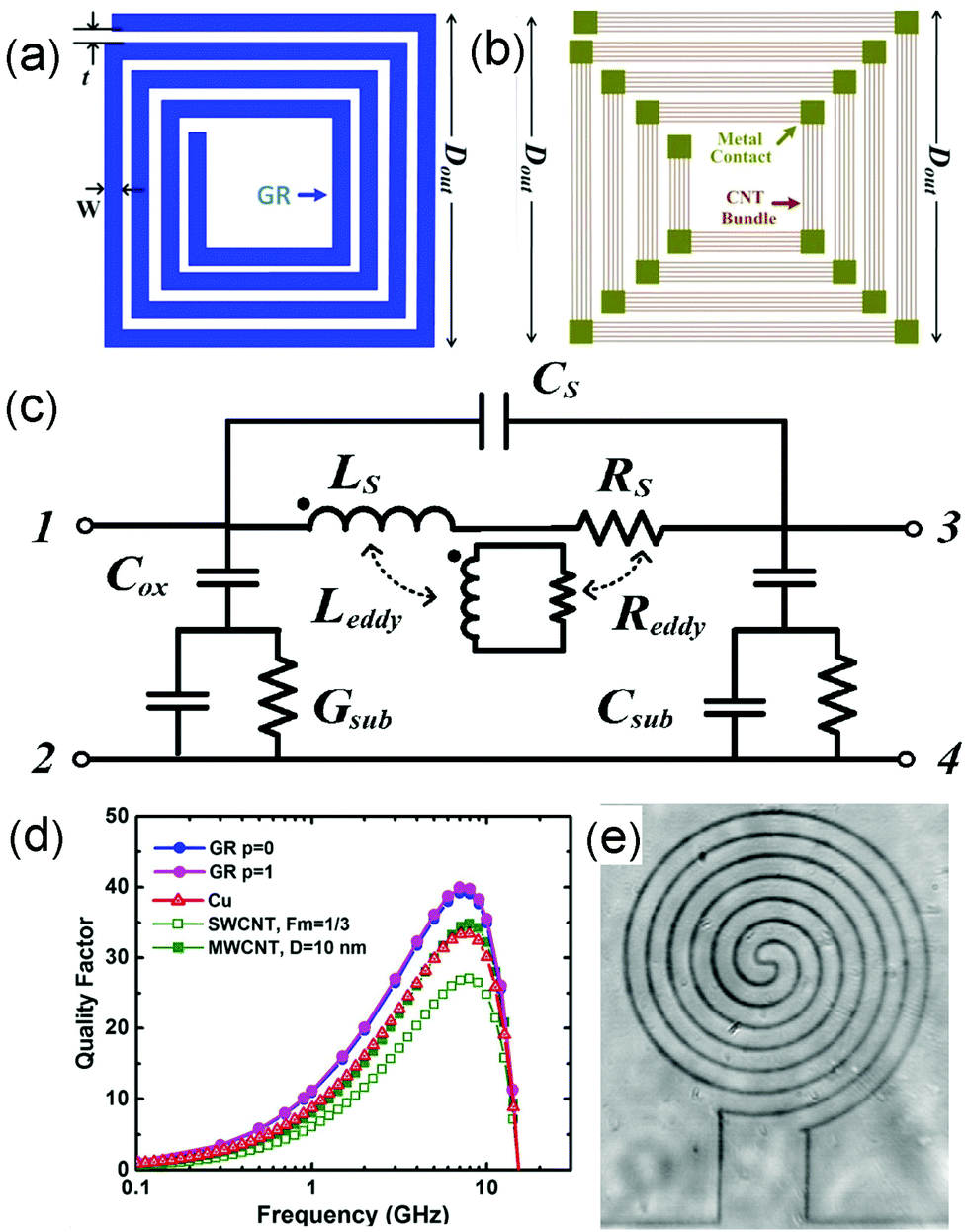 | ||
| Fig. 21 (a) Schematic view of a four-turn spiral graphene-based inductor (b) CNT-based inductor. At each corner, there is a metal contact to connect CNT bundles. However, no such contacts are required for graphene-based inductors. (c) Modified π model for on-chip spiral inductors. In this model, LS and RS are the series frequency-dependent inductance and resistance, respectively. Leddy and Reddy are the eddy-current-induced parameters, and CS, Cox, and Csub are the inter-turn conductor capacitance, the oxide capacitance, and the substrate capacitance, respectively. (d) Q-factors of inductors based on graphene, Cu, single-walled CNT, and multi-walled CNT interconnects as a function of frequency for low-loss (ρsub = 10 Ω cm) substrate. (Taken from ref. 53. Reproduced by permission of the Institute of Electrical and Electronics Engineers (IEEE).) (e) Optical microscopy image of an inductor fabricated via direct imprinting on graphene oxide film using femtosecond laser reduction. (Taken from ref. 54. Reproduced by permission of Elsevier.) | ||
The high frequency effects of graphene inductors have been thoroughly investigated by taking into account the kinetic inductance of graphene, the anomalous skin effect, and edge specularities (Fig. 21).53 Comparative studies with CNT- and copper-based inductors have also been done. The quality factors (Q-factor) of each design were compared using a modified π model (Fig. 21c) of the on-chip inductors (Fig. 21d). A higher Q-factor is desirable because it leads to lower loss and higher frequency stability.94 With a fixed design on a low-loss (high-resistivity; 10 Ω cm) substrate, the Q-factor of the graphene inductor shows an improvement of about 20% compared to that of copper. On the other hand, 50% improvement and 15% improvement were observed with respect to single-walled CNT (with 1/3 metallic fraction) and multi-walled CNT-based inductors, respectively (Fig. 21d). An example of a graphene inductor patterned on graphene oxide films by using the direct femtosecond laser reduction process is shown in Fig. 21e.54
Transition metal dichalcogenides-based circuits
The study of transition metal dichalcogenides is currently a highly active area of research. Fundamental studies of transistor operations have been conducted on some of the more accessible TMDs such as MoS2, WS2, and WSe2 using mechanically exfoliated samples. Transistors with subthreshold slopes reaching 60 mV dec−1 (ref. 87) and mobility values up to 250 cm2 V−1 s−1 (ref. 87) have already been demonstrated. However, to drive the field forward, the development of large-scale synthesis and integration methods is crucial. Unlike graphene, which is usually synthesized on transition metals such as copper or nickel using CVD,18 several TMDs have been successfully synthesized on insulating layers such as glass,25 sapphire,25,27 and silicon dioxide.22,25–27,105 The capability to directly synthesize TMDs on top of a non-conducting substrate is an important step toward system-level integration of these 2D materials. However, it is important to note that the deposition temperature is still quite high (650 °C–800 °C) and the films are polycrystalline.22,23,25–27,105 An effective way to synthesize higher quality, large-area single-crystalline films is still in high demand.Integrated circuits such as inverters,55–58 small signal amplifiers,55 logic gates,56–58 a SRAM cell,57 and a 5-stage ring oscillator57 were demonstrated using both exfoliated55–57 and CVD synthesized58 MoS2 samples.
A small signal amplifier based on a single grain of exfoliated MoS2 samples is shown (Fig. 22). Unlike graphene-based transistors, MoS2 transistors can reach an on/off ratio of 108.2 The transconductance gm reached a value of 12 μS (2.6 μS μm−1) for Vds = 500 mV and gate oxide of HfO2 (30 nm) using optical lithography.55 The small signal amplifiers reached a gain of ∼4 at 2VDD. The device configuration and the transfer characteristics are shown in Fig. 22.
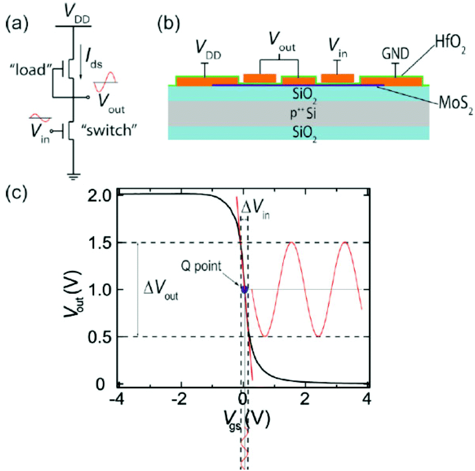 | ||
| Fig. 22 (a) Schematic of an MoS2 amplifier in a common-source configuration. (b) Vertical cross-section of the amplifier. (c) Transfer characteristic of the amplifier. The “switch” transistor is biased at a quiescent point (Q point). The “load” transistor operates as resister at this point. A small AC signal of amplitude ΔVin/2 is then superimposed on the gate bias and amplified. (Taken from ref. 55. Reproduced by permission of the American Institute of Physics.) | ||
An integrated circuit with inverters, logic gates, a SRAM cell, and a 5-stage ring oscillator was also demonstrated with exfoliated bilayer MoS2.57 In Fig. 23a, a flip-flop SRAM circuit with MoS2 transistors can be set to logic state 1 (or 0) by applying a low (or high) voltage to the input. The output logic state stays at 0 or 1 after the switch to the input has been opened, thus serving as a non-volatile memory. In the NAND gate circuit using MoS2 transistors (Fig. 23b), the output of the circuit is close to logic state 1 when either or both of the inputs are at logic state 0. The output is at logic state 0 only when both inputs are at logic state 1 (i.e. when both MoS2 FETs are conducting). The ring oscillator (Fig. 23c) was realized by cascading five inverter stages in a close loop. The transistor gate length Lg was 1 μm (W/Lg ∼ 20). An extra inverter stage was used to synthesize the output signal by isolating the oscillator operation from the measurement setup. At Vdd = 2 V, the fundamental oscillation frequency is at 1.6 MHz, corresponding to a propagation delay of τpd = 1/(2nf) = 62.5 ns per stage, where n is the number of stages and f is the fundamental oscillation frequency. Fig. 23d depicts the power spectrum of the output signal as a function of Vdd. From left to right, Vdd is changed from 1.1 V to 2.0 V in steps of 0.1 V.
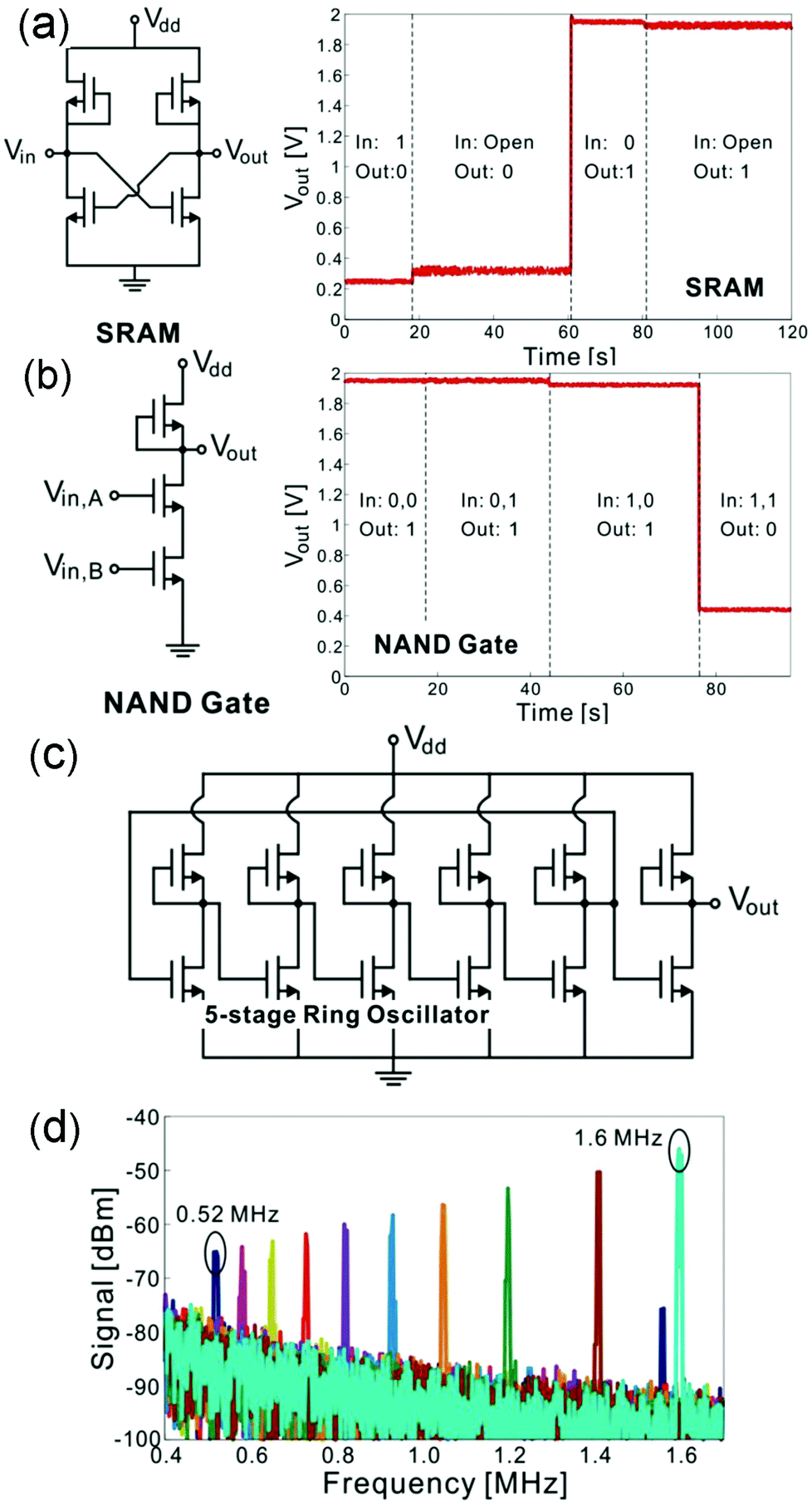 | ||
| Fig. 23 (a) The schematics of the electronic circuits for SRAM, based on exfoliated bilayer MoS2 transistors and its output voltage characteristics. A logic state 1 (or 0) at the input voltage can set the output voltage to logic state 0 (or 1). (b) The schematics of the electronic circuits for NAND gate based on exfoliated bilayer MoS2 transistors, and its output voltage. A low voltage below 0.5 V represents a logic state 0 and a voltage close to 2 V represents a logic state 1. (c) Schematic of the electronic circuit of the 5-stage ring oscillator. The first five inverter stages form the positive feedback loop, and the last inverter serves as the synthesis stage. (d) The power spectrum of the output signal as a function of Vdd. From left to right, Vdd is changed from 1.15 V and 1.2 to 2.0 V in step of 0.1 V. (Taken from ref. 57. Reproduced by permission of the American Chemical Society.) | ||
Conclusions and perspectives
An important advantage of a two-dimensional structure compared to other nanomaterials is the straightforward integration with existing top-down fabrication processes. Although other zero-dimensional and one-dimensional nanostructures were discovered early and investigated for a longer period of time, the difficulty in controlling the exact position and the concentration of these individual nanomaterials was a major obstacle in commercialization for integrated electronics.8 For example, the chirality (directionality of graphitic hexagonal lattice) and the thickness of one-dimensional carbon nanotubes were very important as they determine the bandgap and the electronic behaviour of individual nanotubes.72 Controlling these parameters in carbon nanotubes still remains a key challenge, even after two decades of intense study since their discovery.106,107 On the other hand, with 2D materials, a facile integration of bottom-up nanomaterial synthesis with top-down lithographic fabrication is possible. After 2D materials are transferred onto a substrate, a conventional semiconductor fabrication process can be used to manufacture various devices. This property also allows seamless integration of the current state-of-the-art fabrication technology with 2D materials.Based on the 2013 International Technology Roadmap for Semiconductors (ITRS) executive summary, the advancement of electronic technology can be categorized into two directions: More Moore (elements that scale according to the traditional “Moore's Law”) and More than Moore (elements that add new functionalities [non-CMOS] that do not typically scale or behave according to the “Moore's Law”). Fig. 24 illustrates the potential applications and the challenges associated with the exploitation of the 2D materials in these two distinctive directions.
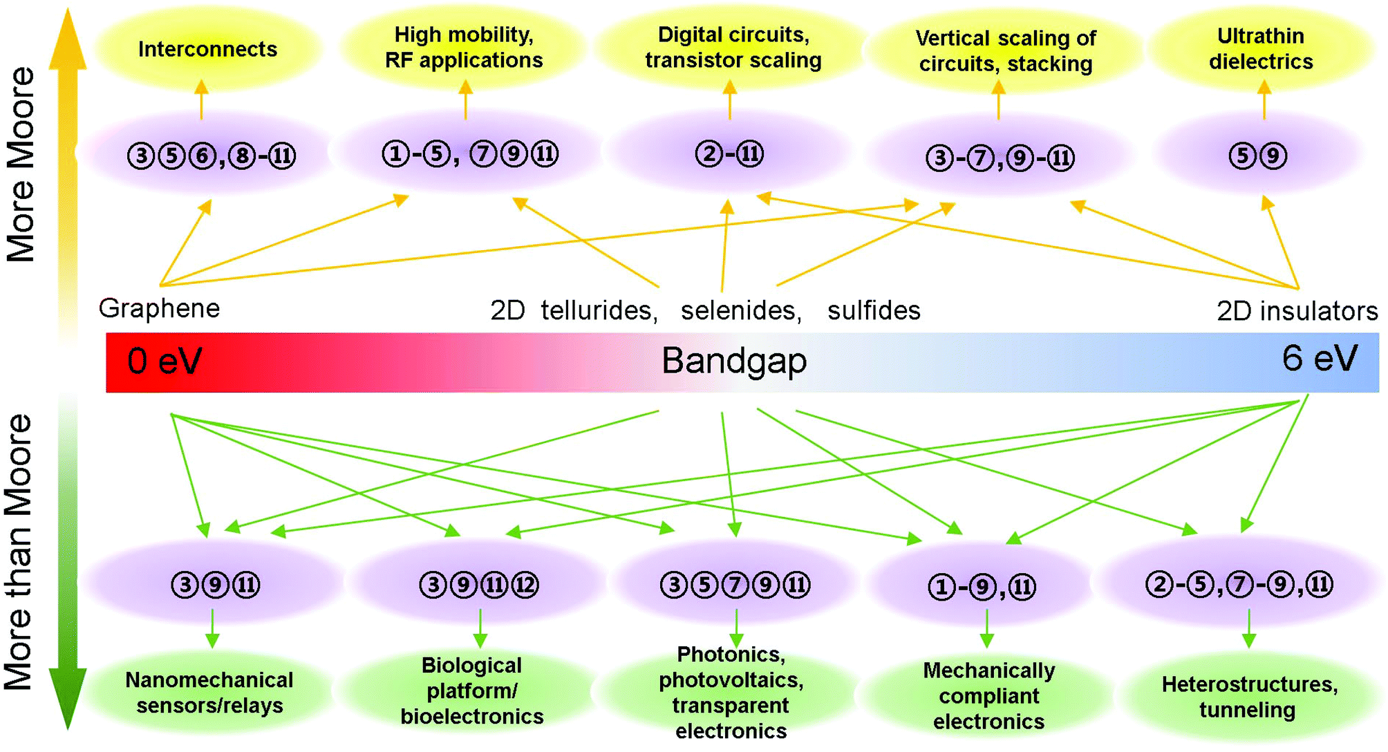 | ||
Fig. 24 Potential applications for 2D materials and the associated challenges.  The lack of current saturation and low gain of graphene transistors. The lack of current saturation and low gain of graphene transistors.  Relatively low mobility (<200 cm2) of 2D transition metal dichalcogenides. Relatively low mobility (<200 cm2) of 2D transition metal dichalcogenides.  Cleaning method to remove polymer/PR residue without using O2 plasma. Cleaning method to remove polymer/PR residue without using O2 plasma.  Pinhole-free dielectric formation. Pinhole-free dielectric formation.  Single crystalline/larger grain size Single crystalline/larger grain size  reusable substrate, waste handling. reusable substrate, waste handling.  Control of contact resistance/Schottky barrier/Fermi level pinning. Control of contact resistance/Schottky barrier/Fermi level pinning.  Effective doping methods stable in air and/or hermetic packaging. Effective doping methods stable in air and/or hermetic packaging.  Reducing defects from thermal coefficient mismatch of the film and the substrate during CVD. Reducing defects from thermal coefficient mismatch of the film and the substrate during CVD.  Low temperature (<400 °C) CVD synthesis for direct growth and integration. Low temperature (<400 °C) CVD synthesis for direct growth and integration.  Clean, repeatable interface after wet/dry transfer or direct synthesis without using metal catalyst. Clean, repeatable interface after wet/dry transfer or direct synthesis without using metal catalyst.  Toxicity. Toxicity. | ||
First, these materials can be utilized as a key component for the continuation of the Moore's law (More Moore, Fig. 24). From the scaling theory, a thin channel is required to minimize the short-channel effects.8 When other semiconducting materials are thinned down to such extreme (<4 nm) thickness, severe performance degradation arises from the surface states and the atomic thickness fluctuation.59–61 In contrast, naturally thin, inert 2D films with no dangling bonds can be highly effective in the lateral scaling (e.g. transistor scaling) and the vertical scaling (e.g. stacking of electronic components) of the electronic components.8,47,108 Ultrathin but highly functional interconnects and dielectrics are also essential to the continuation of Moore's law.
Second, with so many unique features available from different sets of 2D materials with various thicknesses, myriad possibilities emerge for unique functionalities (More than Moore, Fig. 24). This is especially true for components that require atomically sharp interfaces and smoothness, such as superlattices/heterostructure FETs,95 optoelectronic components,1,95,103 and photovoltaics.109 Various atomic layered heterostructures with 2D building blocks exhibited highly interesting characteristics due to quantum confinement and low density of states. For example, several heterostructures were used to make extremely thin (<10 nm) vertical transistors that depend on the modulation of barrier heights through a vertical E-field.110,111 In addition, Van Hove singularities in the electronic density of states of TMDs result in enhanced light–matter interactions, leading to enhanced photon absorption and electron–hole creation.109 Consequently, extremely efficient photovoltaic (external quantum efficiency >30%)109 and ultrahigh gain (>108) photodetectors112 based on 2D heterostructures were demonstrated.
Since these materials can also be transferred to an arbitrary substrate, the possibility of utilizing exotic substrates such as plastics opens up doors for novel applications in both electronics and photonics.1,103 The mechanical robustness, flexibility, and transparency of the material will be indispensable for niche applications such as ultrathin displays,103 mechanically compliant electronics,37,52 photovoltaics,1,103 biomedical applications,113 transparent electronics,34 and nano-mechanical systems.114
Finally, several key challenges need to be addressed before 2D materials can be fully adopted into the mainstream technology. First, the growth temperature of these materials usually exceeds 600 °C.22,25,27 Such a high temperature process is not always compatible with various fabrication steps. Furthermore, although film transfer is possible, a meticulous cleaning process is necessary during the wet transfers to achieve high quality interfaces.77 After the transfer and the following lithography steps, removing polymer residue without using O2 plasma is another challenge. (O2 plasma is known to etch 2D materials.37,58) Second, either single-crystalline films or polycrystalline films with large grain boundaries are desirable for most electronics. Currently, most large-area films are polycrystalline with small grain boundaries,22,26,27,105 and most single-crystalline films are discontinuous (i.e. flakes).25,105 Defect control during the high temperature synthesis phase is also difficult. For example, the thermal expansion coefficient mismatch between the film and the substrate will result in residual thermal stress on the 2D films, which is responsible for defects and wrinkles.115 Third, forming good ohmic contacts with extremely thin semiconductors is a great challenge.116–119 Many TMDs (e.g. MoS2), being large bandgap materials, aggravate the problem.116 A promising method for assembling a superior ohmic contact with TMDs (e.g. MoS2) is to use graphene as the contact material.120,121 Not only was the barrier height of the graphene/MoS2 interface determined to be lower than the popular Ti/MoS2 contact,121 but the E-field-induced Fermi level control via the gate120 was found to be a promising way to produce a near-ohmic contact with higher on-state current. Fourth, doping these materials is not trivial since conventional interstitial doping will introduce defects. An alternative method is to exploit the charge transfer characteristics of different adsorbates. Various gas molecules were found to have a profound effect on the electrical transport properties of 2D films.92,122 For example, H2, O2, and H2O were found to work as charge acceptors in MoS2 after adsorption. Gases such as NH3 were found to be charge donors.122 However, retaining the gas molecules and their charge transfer qualities in ambient air over a prolonged time was found to be difficult to achieve.119 In addition, the various unintentional surface adsorbates from the environment may limit the performance of 2D films. Fifth, the highly inert surfaces of 2D materials render it difficult to form a pinhole-free dielectric with atomic layer deposition.123 A seed layer using PVD124 or spin coating123 is sometimes necessary, and optimization of this multilayer dielectric is required. Some of the mentioned challenges are much more critical in certain applications. An overview illustrated in Fig. 24 addresses some of the more pressing challenges for different applications.
It is difficult to determine specific timelines for each of these applications with many practical issues still waiting to be addressed. However, dealing with these issues is currently an active area of research, and recent progress shows great promise.87,117,118,125,126 It is safe to assume that initial applications will consist of both 2D materials and conventional bulk materials. However, an ultra-thin electronic system exclusively assembled with 2D materials127 is also plausible since various 2D materials with different electronic properties are now available. With the continued improvements in large-scale synthesis and integration, 2D materials will be a vital component for advanced circuits and systems in the near future.
Acknowledgements
Acknowledgement is made to the National Science Foundation Scalable Nanomanufacturing Program (DMR-1120187) and NSF CAREER Award (ECCS-1254468).Notes and references
- Q. H. Wang, K. Kalantar-Zadeh, A. Kis, J. N. Coleman and M. S. Strano, Nat. Nanotechnol., 2012, 7, 699–712 CrossRef CAS PubMed.
- B. Radisavljevic, A. Radenovic, J. Brivio, V. Giacometti and A. Kis, Nat. Nanotechnol., 2011, 6, 147–150 CrossRef CAS PubMed.
- R. Mas-Balleste, C. Gomez-Navarro, J. Gomez-Herrero and F. Zamora, Nanoscale, 2011, 3, 20–30 RSC.
- A. K. Geim and K. S. Novoselov, Nat. Mater., 2007, 6, 183–191 CrossRef CAS PubMed.
- K. Novoselov, A. K. Geim, S. Morozov, D. Jiang, M. Katsnelson, I. Grigorieva, S. Dubonos and A. Firsov, Nature, 2005, 438, 197–200 CrossRef CAS PubMed.
- A. K. Geim, Science, 2009, 324, 1530–1534 CrossRef CAS PubMed.
- M. Chhowalla, H. S. Shin, G. Eda, L.-J. Li, K. P. Loh and H. Zhang, Nat. Chem., 2013, 5, 263–275 CrossRef PubMed.
- F. Schwierz, Nat. Nanotechnol., 2010, 5, 487–496 CrossRef CAS PubMed.
- K. S. Novoselov, A. K. Geim, S. Morozov, D. Jiang, Y. Zhang, S. Dubonos, I. Grigorieva and A. Firsov, Science, 2004, 306, 666–669 CrossRef CAS PubMed.
- X. Du, I. Skachko, A. Barker and E. Y. Andrei, Nat. Nanotechnol., 2008, 3, 491–495 CrossRef CAS PubMed.
- R. Nair, P. Blake, A. Grigorenko, K. Novoselov, T. Booth, T. Stauber, N. Peres and A. Geim, Science, 2008, 320, 1308–1308 CrossRef CAS PubMed.
- W. Wu, L. A. Jauregui, Z. Su, Z. Liu, J. Bao, Y. P. Chen and Q. Yu, Adv. Mater., 2011, 23, 4898–4903 CrossRef CAS PubMed.
- X. Ding, G. Ding, X. Xie, F. Huang and M. Jiang, Carbon, 2011, 49, 2522–2525 CrossRef CAS PubMed.
- C. Mattevi, H. Kim and M. Chhowalla, J. Mater. Chem., 2011, 21, 3324–3334 RSC.
- C.-Y. Su, A.-Y. Lu, C.-Y. Wu, Y.-T. Li, K.-K. Liu, W. Zhang, S.-Y. Lin, Z.-Y. Juang, Y.-L. Zhong and F.-R. Chen, Nano Lett., 2011, 11, 3612–3616 CrossRef CAS PubMed.
- Q. Yu, L. A. Jauregui, W. Wu, R. Colby, J. Tian, Z. Su, H. Cao, Z. Liu, D. Pandey and D. Wei, Nat. Mater., 2011, 10, 443–449 CrossRef CAS PubMed.
- X. Li, W. Cai, J. An, S. Kim, J. Nah, D. Yang, R. Piner, A. Velamakanni, I. Jung, E. Tutuc, S. K. Banerjee, L. Colombo and R. S. Ruoff, Science, 2009, 324, 1312–1314 CrossRef CAS PubMed.
- S. Lee, K. Lee and Z. Zhong, Nano Lett., 2010, 10, 4702–4707 CrossRef CAS PubMed.
- A. Reina, X. Jia, J. Ho, D. Nezich, H. Son, V. Bulovic, M. S. Dresselhaus and J. Kong, Nano Lett., 2008, 9, 30–35 CrossRef PubMed.
- W. Strupinski, K. Grodecki, A. Wysmolek, R. Stepniewski, T. Szkopek, P. Gaskell, A. Gruneis, D. Haberer, R. Bozek and J. Krupka, Nano Lett., 2011, 11, 1786–1791 CrossRef CAS PubMed.
- A. Guermoune, T. Chari, F. Popescu, S. S. Sabri, J. Guillemette, H. S. Skulason, T. Szkopek and M. Siaj, Carbon, 2011, 49, 4204–4210 CrossRef CAS PubMed.
- Y. H. Lee, X. Q. Zhang, W. Zhang, M. T. Chang, C. T. Lin, K. D. Chang, Y. C. Yu, J. T. W. Wang, C. S. Chang and L. J. Li, Adv. Mater., 2012, 24, 2320–2325 CrossRef CAS PubMed.
- W. Y. Lee, T. M. Besmann and M. W. Stott, J. Mater. Res., 1994, 9, 1474–1483 CrossRef CAS.
- J. Cheon, J. E. Gozum and G. S. Girolami, Chem. Mater., 1997, 9, 1847–1853 CrossRef CAS.
- S. Wu, C. Huang, G. Aivazian, J. S. Ross, D. H. Cobden and X. Xu, ACS Nano, 2013, 7, 2768–2772 CrossRef CAS PubMed.
- Y. Zhan, Z. Liu, S. Najmaei, P. M. Ajayan and J. Lou, Small, 2012, 8, 966–971 CrossRef CAS PubMed.
- K.-K. Liu, W. Zhang, Y.-H. Lee, Y.-C. Lin, M.-T. Chang, C.-Y. Su, C.-S. Chang, H. Li, Y. Shi and H. Zhang, Nano Lett., 2012, 12, 1538 CrossRef CAS PubMed.
- Y.-H. Lee, L. Yu, H. Wang, W. Fang, X. Ling, Y. Shi, C.-T. Lin, J.-K. Huang, M.-T. Chang and C.-S. Chang, Nano Lett., 2013, 13, 1852 CAS.
- Y. Wu, Y.-m. Lin, A. A. Bol, K. A. Jenkins, F. Xia, D. B. Farmer, Y. Zhu and P. Avouris, Nature, 2011, 472, 74–78 CrossRef CAS PubMed.
- L. Liao, Y.-C. Lin, M. Bao, R. Cheng, J. Bai, Y. Liu, Y. Qu, K. L. Wang, Y. Huang and X. Duan, Nature, 2010, 467, 305–308 CrossRef CAS PubMed.
- F. Schwierz, Nature, 2011, 472, 41–42 CrossRef CAS PubMed.
- F. Schwierz, Proc. IEEE, 2013, 101, 1567–1584 CrossRef CAS.
- F. Schwierz, VLSI Technology, Systems and Applications (VLSI-TSA), 2011 International Symposium on, 2011, pp. 1–2.
- H. Wang, D. Nezich, J. Kong and T. Palacios, IEEE Electron Device Lett., 2009, 30, 547–549 CrossRef CAS.
- X. Yang, G. Liu, A. A. Balandin and K. Mohanram, ACS Nano, 2010, 4, 5532–5538 CrossRef CAS PubMed.
- Z. Wang, Z. Zhang, H. Xu, L. Ding, S. Wang and L.-M. Peng, Appl. Phys. Lett., 2010, 96, 173104 CrossRef PubMed.
- S. Lee, K. Lee, C.-H. Liu, G. S. Kulkarni and Z. Zhong, Nat. Commun., 2012, 3, 1018 CrossRef PubMed.
- H. Wang, A. Hsu, J. Wu, J. Kong and T. Palacios, IEEE Electron Device Lett., 2010, 31, 906–908 CrossRef CAS.
- Y.-M. Lin, A. Valdes-Garcia, S.-J. Han, D. B. Farmer, I. Meric, Y. Sun, Y. Wu, C. Dimitrakopoulos, A. Grill and P. Avouris, Science, 2011, 332, 1294–1297 CrossRef CAS PubMed.
- O. Habibpour, S. Cherednichenko, J. Vukusic, K. Yhland and J. Stake, IEEE Electron Device Lett., 2012, 33, 71–73 CrossRef CAS.
- E. Guerriero, L. Polloni, L. G. Rizzi, M. Bianchi, G. Mondello and R. Sordan, Small, 2012, 8, 357–361 CrossRef CAS.
- Y. Wu, K. A. Jenkins, A. Valdes-Garcia, D. B. Farmer, Y. Zhu, A. A. Bol, C. Dimitrakopoulos, W. Zhu, F. Xia and P. Avouris, Nano Lett., 2012, 12, 3062–3067 CrossRef CAS PubMed.
- S.-J. Han, K. A. Jenkins, A. Valdes Garcia, A. D. Franklin, A. A. Bol and W. Haensch, Nano Lett., 2011, 11, 3690–3693 CrossRef CAS PubMed.
- S.-J. Han, A. V. Garcia, S. Oida, K. A. Jenkins and W. Haensch, Nat. Commun., 2014, 5, 3086 Search PubMed.
- N. Harada, K. Yagi, S. Sato and N. Yokoyama, Appl. Phys. Lett., 2010, 96, 012102 CrossRef PubMed.
- H.-Y. Chen and J. Appenzeller, Nano Lett., 2012, 12, 2067–2070 CrossRef CAS PubMed.
- X. Chen, D. Akinwande, K.-J. Lee, G. F. Close, S. Yasuda, B. C. Paul, S. Fujita, J. Kong and H.-S. Wong, IEEE Trans. Electron Devices, 2010, 57, 3137–3143 CrossRef CAS.
- S. L. Li, H. Miyazaki, M. V. Lee, C. Liu, A. Kanda and K. Tsukagoshi, Small, 2011, 7, 1552–1556 CrossRef CAS PubMed.
- S.-L. Li, H. Miyazaki, A. Kumatani, A. Kanda and K. Tsukagoshi, Nano Lett., 2010, 10, 2357–2362 CrossRef CAS PubMed.
- L. G. Rizzi, M. Bianchi, A. Behnam, E. Carrion, E. Guerriero, L. Polloni, E. Pop and R. Sordan, Nano Lett., 2012, 12, 3948–3953 CrossRef CAS PubMed.
- Q. Shao, G. Liu, D. Teweldebrhan and A. Balandin, Appl. Phys. Lett., 2008, 92, 202108 CrossRef PubMed.
- S. Lee, K. Lee, C.-H. Liu and Z. Zhong, Nanoscale, 2012, 4, 639–644 RSC.
- D. Sarkar, C. Xu, H. Li and K. Banerjee, IEEE Trans. Electron Devices, 2011, 58, 853–859 CrossRef CAS.
- Y. Zhang, L. Guo, S. Wei, Y. He, H. Xia, Q. Chen, H.-B. Sun and F.-S. Xiao, Nano Today, 2010, 5, 15–20 CrossRef CAS PubMed.
- B. Radisavljevic, M. B. Whitwick and A. Kis, Appl. Phys. Lett., 2012, 101, 043103 CrossRef PubMed.
- B. Radisavljevic, M. B. Whitwick and A. Kis, ACS Nano, 2011, 5, 9934–9938 CrossRef CAS PubMed.
- H. Wang, L. Yu, Y.-H. Lee, Y. Shi, A. Hsu, M. L. Chin, L.-J. Li, M. Dubey, J. Kong and T. Palacios, Nano Lett., 2012, 12, 4674–4680 CrossRef CAS PubMed.
- H. Wang, L. Yu, Y.-H. Lee, W. Fang, A. Hsu, P. Herring, M. Chin, M. Dubey, L.-J. Li and J. Kong, APS March Meeting Abstracts, 2013, p. 7009.
- K. Uchida, H. Watanabe, A. Kinoshita, J. Koga, T. Numata and S. Takagi, Electron Devices Meeting, 2002. IEDM'02. International IEEE, 2002, pp. 47–50.
- L. Gomez, I. Aberg and J. Hoyt, IEEE Electron Device Lett., 2007, 28, 285–287 CrossRef CAS.
- K. Uchida and S.-i. Takagi, Appl. Phys. Lett., 2003, 82, 2916–2918 CrossRef CAS PubMed.
- V. Suntharalingam, R. Berger, J. A. Burns, C. K. Chen, C. L. Keast, J. M. Knecht, R. D. Lambert, K. L. Newcomb, D. M. O'Mara and D. D. Rathman, Solid-State Circuits Conference, 2005. Digest of Technical Papers. ISSCC. IEEE International, 2005, pp. 356–357.
- R. S. Patti, Proc. IEEE, 2006, 94, 1214–1224 CrossRef.
- J. Burns, L. McIlrath, C. Keast, C. Lewis, A. Loomis, K. Warner and P. Wyatt, Solid-State Circuits Conference, 2001. Digest of Technical Papers. ISSCC. IEEE International, 2001, pp. 268–269.
- J. Kang, S. Tongay, J. Zhou, J. Li and J. Wu, Appl. Phys. Lett., 2013, 102, 012111 CrossRef PubMed.
- A. Splendiani, L. Sun, Y. Zhang, T. Li, J. Kim, C.-Y. Chim, G. Galli and F. Wang, Nano Lett., 2010, 10, 1271–1275 CrossRef CAS PubMed.
- K. Watanabe, T. Taniguchi and H. Kanda, Nat. Mater., 2004, 3, 404 CrossRef CAS PubMed.
- R. R. Nair, W. Ren, R. Jalil, I. Riaz, V. G. Kravets, L. Britnell, P. Blake, F. Schedin, A. S. Mayorov and S. Yuan, Small, 2010, 6, 2877–2884 CrossRef CAS PubMed.
- M. I. Katsnelson, Mater. Today, 2007, 10, 20–27 CrossRef CAS.
- P. R. Wallace, Phys. Rev., 1947, 71, 622 CrossRef CAS.
- J. Slonczewski and P. Weiss, Phys. Rev., 1958, 109, 272 CrossRef CAS.
- A. C. Neto, F. Guinea, N. Peres, K. S. Novoselov and A. K. Geim, Rev. Mod. Phys., 2009, 81, 109 CrossRef.
- G. W. Semenoff, Phys. Rev. Lett., 1984, 53, 2449–2452 CrossRef.
- M. Freitag, Nat. Nanotechnol., 2008, 3, 455–457 CrossRef CAS PubMed.
- M. Trushin and J. Schliemann, Phys. Rev. Lett., 2007, 99, 216602 CrossRef.
- M. Katsnelson, Eur. Phys. J. B, 2006, 51, 157–160 CrossRef CAS.
- S. Morozov, K. Novoselov, M. Katsnelson, F. Schedin, D. Elias, J. Jaszczak and A. Geim, Phys. Rev. Lett., 2008, 100, 016602 CrossRef CAS.
- K. Bolotin, K. Sikes, J. Hone, H. Stormer and P. Kim, Phys. Rev. Lett., 2008, 101, 096802 CrossRef CAS.
- E. V. Castro, H. Ochoa, M. Katsnelson, R. Gorbachev, D. Elias, K. Novoselov, A. Geim and F. Guinea, 2010, arXiv preprint arXiv:1008.2522.
- A. S. Mayorov, R. V. Gorbachev, S. V. Morozov, L. Britnell, R. Jalil, L. A. Ponomarenko, P. Blake, K. S. Novoselov, K. Watanabe and T. Taniguchi, Nano Lett., 2011, 11, 2396–2399 CrossRef CAS PubMed.
- K. Nomura and A. MacDonald, Phys. Rev. Lett., 2007, 98, 076602 CrossRef.
- M. Katsnelson and A. Geim, Philos. Trans. R. Soc. London, Ser. A, 2008, 366, 195 CrossRef CAS PubMed.
- R. Coehoorn, C. Haas, J. Dijkstra, C. Flipse, R. De Groot and A. Wold, Phys. Rev. B: Condens. Matter, 1987, 35, 6195 CrossRef CAS.
- H. Zhang, E. Bekyarova, J.-W. Huang, Z. Zhao, W. Bao, F. Wang, R. C. Haddon and C. N. Lau, Nano Lett., 2011, 11, 4047–4051 CrossRef CAS PubMed.
- D. B. Farmer, H.-Y. Chiu, Y.-M. Lin, K. A. Jenkins, F. Xia and P. Avouris, Nano Lett., 2009, 9, 4474–4478 CrossRef CAS PubMed.
- K. I. Bolotin, K. Sikes, Z. Jiang, M. Klima, G. Fudenberg, J. Hone, P. Kim and H. Stormer, Solid State Commun., 2008, 146, 351–355 CrossRef CAS PubMed.
- H. Fang, S. Chuang, T. C. Chang, K. Takei, T. Takahashi and A. Javey, Nano Lett., 2012, 12, 3788–3792 CrossRef CAS PubMed.
- A. L. Elías, N. Perea-López, A. s. Castro-Beltrán, A. Berkdemir, R. Lv, S. Feng, A. D. Long, T. Hayashi, Y. A. Kim and M. Endo, ACS Nano, 2013, 7, 5235–5242 CrossRef PubMed.
- R. Coehoorn, C. Haas and R. De Groot, Phys. Rev. B: Condens. Matter, 1987, 35, 6203 CrossRef CAS.
- G. Eda, T. Fujita, H. Yamaguchi, D. Voiry, M. Chen and M. Chhowalla, ACS Nano, 2012, 6, 7311–7317 CrossRef CAS PubMed.
- C.-H. Lee, G.-H. Lee, A. M. van der Zande, W. Chen, Y. Li, M. Han, X. Cui, G. Arefe, C. Nuckolls and T. F. Heinz, 2014, arXiv preprint arXiv:1403.3062.
- S. Tongay, J. Zhou, C. Ataca, J. Liu, J. S. Kang, T. S. Matthews, L. You, J. Li, J. C. Grossman and J. Wu, Nano Lett., 2013, 13, 2831 CrossRef CAS PubMed.
- M. Abbasi, R. Kozhuharov, C. Karnfelt, I. Angelov, I. Kallfass, P. Leuther and H. Zirath, IEEE Trans. Microw. Theory Tech., 2009, 57, 3134–3142 CrossRef CAS.
- T. H. Lee, The design of CMOS radio-frequency integrated circuits, Cambridge university press, 2004 Search PubMed.
- S. M. Sze and K. K. Ng, Physics of semiconductor devices, John Wiley & Sons, 2006 Search PubMed.
- Y. Awano, Electron Devices Meeting (IEDM), 2009 IEEE International IEEE, 2009, pp. 1–4.
- Y. Meng, Y. Zhao, C. Hu, H. Cheng, Y. Hu, Z. Zhang, G. Shi and L. Qu, Adv. Mater., 2013, 25, 2326–2331 CrossRef CAS PubMed.
- T. T. Tung, M. Castro, T. Y. Kim, K. S. Suh and J.-F. Feller, J. Mater. Chem., 2012, 22, 21754–21766 RSC.
- M. Nihei, A. Kawabata, D. Kondo, M. Horibe, S. Sato and Y. Awano, Jpn. J. Appl. Phys., 2005, 44, 1626 CrossRef CAS.
- P. Blake, P. D. Brimicombe, R. R. Nair, T. J. Booth, D. Jiang, F. Schedin, L. A. Ponomarenko, S. V. Morozov, H. F. Gleeson and E. W. Hill, Nano Lett., 2008, 8, 1704–1708 CrossRef PubMed.
- S. Bae, H. Kim, Y. Lee, X. Xu, J.-S. Park, Y. Zheng, J. Balakrishnan, T. Lei, H. R. Kim and Y. I. Song, Nat. Nanotechnol., 2010, 5, 574 CrossRef CAS PubMed.
- Y. Zhu, Z. Sun, Z. Yan, Z. Jin and J. M. Tour, ACS Nano, 2011, 5, 6472–6479 CrossRef CAS PubMed.
- F. Bonaccorso, Z. Sun, T. Hasan and A. Ferrari, Nat. Photonics, 2010, 4, 611–622 CrossRef CAS.
- J. K. Wassei and R. B. Kaner, Mater. Today, 2010, 13, 52–59 CrossRef CAS.
- S. Najmaei, Z. Liu, W. Zhou, X. Zou, G. Shi, S. Lei, B. I. Yakobson, J.-C. Idrobo, P. M. Ajayan and J. Lou, Nat. Mater., 2013, 12, 754–759 CrossRef CAS PubMed.
- H. Dai, Surf. Sci., 2002, 500, 218–241 CrossRef CAS.
- H. Wei, M. Shulaker, G. Hills, H.-Y. Chen, C.-S. Lee, L. Liyanage, J. Zhang, H.-S. P. Wong and S. Mitra Design, Automation & Test in Europe Conference & Exhibition (DATE), 2013 IEEE, 2013, p. 619.
- W. Zhu, T. Low, Y.-H. Lee, H. Wang, D. B. Farmer, J. Kong, F. Xia and P. Avouris, Nat. Commun., 2014, 5, 3087 Search PubMed.
- L. Britnell, R. Ribeiro, A. Eckmann, R. Jalil, B. Belle, A. Mishchenko, Y.-J. Kim, R. Gorbachev, T. Georgiou and S. Morozov, Science, 2013, 340, 1311–1314 CrossRef CAS PubMed.
- L. Britnell, R. Gorbachev, R. Jalil, B. Belle, F. Schedin, A. Mishchenko, T. Georgiou, M. Katsnelson, L. Eaves and S. Morozov, Science, 2012, 335, 947–950 CrossRef CAS PubMed.
- H. Yang, J. Heo, S. Park, H. J. Song, D. H. Seo, K.-E. Byun, P. Kim, I. Yoo, H.-J. Chung and K. Kim, Science, 2012, 336, 1140–1143 CrossRef CAS PubMed.
- W. Zhang, C.-P. Chuu, J.-K. Huang, C.-H. Chen, M.-L. Tsai, Y.-H. Chang, C.-T. Liang, Y.-Z. Chen, Y.-L. Chueh and J.-H. He, Sci. Rep., 2014, 4, 3826 Search PubMed.
- Y. Zhang, T. R. Nayak, H. Hong and W. Cai, Nanoscale, 2012, 4, 3833–3842 RSC.
- N. N. Klimov, S. Jung, S. Zhu, T. Li, C. A. Wright, S. D. Solares, D. B. Newell, N. B. Zhitenev and J. A. Stroscio, Science, 2012, 336, 1557–1561 CrossRef CAS PubMed.
- S. J. Chae, F. Güneş, K. K. Kim, E. S. Kim, G. H. Han, S. M. Kim, H. J. Shin, S. M. Yoon, J. Y. Choi and M. H. Park, Adv. Mater., 2009, 21, 2328–2333 CrossRef CAS.
- I. Popov, G. Seifert and D. Tománek, Phys. Rev. Lett., 2012, 108, 156802 CrossRef.
- J.-R. Chen, P. M. Odenthal, A. G. Swartz, G. C. Floyd, H. Wen, K. Y. Luo and R. K. Kawakami, Nano Lett., 2013, 13, 3106–3110 CrossRef CAS PubMed.
- W. Liu, J. Kang, D. Sarkar, Y. Khatami, D. Jena and K. Banerjee, Nano Lett., 2013, 13, 1983–1990 CrossRef CAS PubMed.
- S. McDonnell, R. Addou, C. Buie, R. M. Wallace and C. L. Hinkle, ACS Nano, 2014, 8, 2880 CrossRef CAS PubMed.
- Y. T. Lee, K. Choi, H. S. Lee, S. W. Min, P. J. Jeon, D. K. Hwang, H. J. Choi and S. Im, Small, 2014, 12, 2356–2361 CrossRef PubMed.
- J. Y. Kwak, J. Hwang, B. Calderon, H. Alsalman, N. Munoz, B. Schutter and M. G. Spencer, Nano Lett., 2014, 14, 4511–4516 CrossRef CAS PubMed.
- Q. Yue, Z. Shao, S. Chang and J. Li, Nanoscale Res. Lett., 2013, 8, 1 CrossRef PubMed.
- F. Xia, D. B. Farmer, Y.-m. Lin and P. Avouris, Nano Lett., 2010, 10, 715–718 CrossRef CAS PubMed.
- A. Hsu, H. Wang, K. K. Kim, J. Kong and T. Palacios, IEEE Electron Device Lett., 2011, 32, 1008–1010 CrossRef CAS.
- S. Das, H.-Y. Chen, A. V. Penumatcha and J. Appenzeller, Nano Lett., 2012, 13, 100–105 CrossRef PubMed.
- H. Fang, M. Tosun, G. Seol, T. C. Chang, K. Takei, J. Guo and A. Javey, Nano Lett., 2013, 13, 1991–1995 CrossRef CAS PubMed.
- T. Roy, M. Tosun, J. S. Kang, A. B. Sachid, S. Desai, M. Hettick, C. C. Hu and A. Javey, ACS Nano, 2014, 8, 6259 CrossRef CAS PubMed.
| This journal is © The Royal Society of Chemistry 2014 |