
 Open Access Article
 This Open Access Article is licensed under a Creative Commons Attribution-Non Commercial 3.0 Unported Licence
The search for the most stable structures of silicon–carbon monolayer compounds†
Pengfei
Li
a,
Rulong
Zhou
*b and
Xiao Cheng
Zeng
*ac
aDepartment of Chemical Physics, University of Science and Technology of China, Hefei, Anhui 230026, P. R. China. E-mail: xzeng1@unl.edu
bSchool of Science and Engineering of Materials, Hefei University of Technology, Hefei, Anhui 230009, P. R. China. E-mail: rlzhou@hfut.edu.cn
cDepartment of Chemistry and Nebraska Center for Materials and Nanoscience, University of Nebraska-Lincoln, Lincoln, Nebraska 68588, USA
First published on 5th August 2014
Abstract
The most stable structures of two-dimensional (2D) silicon–carbon monolayer compounds with different stoichiometric compositions (i.e., Si![[thin space (1/6-em)]](https://www.rsc.org/images/entities/char_2009.gif) :C ratio = 2:3, 1:3 and 1:4) are predicted for the first time based on the particle-swarm optimization (PSO) technique combined with density functional theory optimization. Although the 2D Si–C monolayer compounds considered here are rich in carbon, many of the low-energy metastable and the lowest-energy silicon–carbon structures are not graphene (carbon monolayer) like. Phonon-spectrum calculations and ab initio molecular dynamics simulations were also performed to confirm the dynamical stability of the predicted most stable 2D silicon–carbon structures as well their thermal stability at elevated temperature. The computed electronic band structures show that all three predicted silicon–carbon compounds are semiconductors with direct or indirect bandgaps. Importantly, their bandgaps are predicted to be close to those of bulk silicon or bulk germanium. If confirmed in the laboratory, these 2D silicon–carbon compounds with different stoichiometric compositions may be exploited for future applications in nanoelectronic devices.
:C ratio = 2:3, 1:3 and 1:4) are predicted for the first time based on the particle-swarm optimization (PSO) technique combined with density functional theory optimization. Although the 2D Si–C monolayer compounds considered here are rich in carbon, many of the low-energy metastable and the lowest-energy silicon–carbon structures are not graphene (carbon monolayer) like. Phonon-spectrum calculations and ab initio molecular dynamics simulations were also performed to confirm the dynamical stability of the predicted most stable 2D silicon–carbon structures as well their thermal stability at elevated temperature. The computed electronic band structures show that all three predicted silicon–carbon compounds are semiconductors with direct or indirect bandgaps. Importantly, their bandgaps are predicted to be close to those of bulk silicon or bulk germanium. If confirmed in the laboratory, these 2D silicon–carbon compounds with different stoichiometric compositions may be exploited for future applications in nanoelectronic devices.
Introduction
Since the successful isolation of graphene sheets in 2004,1–5 this honeycomb structured 2D material has inspired intensive research interests largely due to its remarkable electronic, mechanical, and optical properties, including its unconventional quantum Hall effect, superior electronic conductivity, and high mechanical strength. In particular, the unique electronic properties of graphene draw attention to this 2D material as a potential candidate for applications in faster and smaller electronic devices. Like carbon, silicon is another group-IV element and also possesses a 2D allotrope with a honeycomb structure, namely silicene. Unlike the graphene sheet which is flat, the silicene sheet exhibits a weakly-buckled local geometry.6,7 However, the zero-bandgap characteristics of both graphene and silicene prevent the direct use of both of these 2D sheets in controlled and reliable transistor operation, which hinder their wide applications in future optoelectronic devices. To date, much effort has been devoted to opening a bandgap (in the 1.0–2.0 eV range) in either graphene or silicene sheets,8–12 although this is still a challenging task as it would require making some major changes to their intrinsic semi-metallic properties originating from the massless Dirac-fermion-like charge carriers.The desire for the continuous miniaturization of electronic devices calls for the development of new and novel low-dimensional materials. Besides graphene and silicene, a wide range of 2D materials, particularly monolayer sheets with atomic thickness, have been reported in the literature. Coleman et al.13 developed a liquid exfoliation technique that can efficiently produce monolayer 2D nanosheets from a variety of inorganic layered materials such as boron nitride (BN), molybdenum disulfide (MoS2), tungsten disulfide (WS2), molybdenum diselenide (MoSe2) and molybdenum telluride (MoTe2). Using a modified liquid exfoliation technique, Xie et al. successfully fabricated monolayer vanadium disulfide (VS2) and tin disulfide (SnS2) in the laboratory.14–16 On the theoretical side, increasing efforts have been devoted to predicting the structures and functional properties of novel 2D materials, such as monolayer boron sheets with low-buckled configurations,17,18 monolayer boron–carbon (BC) compounds,19,20 boron–silicon (BSi) compounds,21 aluminum carbon (AlC) compounds,22 carbon nitride (CN),23 germanene,24,25 tetragonal TiC,26 SnC27 and other group III–VI compounds.27,28
2D silicon–carbon (Si–C) monolayers can be viewed as composition-tunable materials between the pure 2D carbon monolayer – graphene – and the pure 2D silicon monolayer – silicene. Efforts have been made towards predicting the most stable structures of the SiC sheet. Recently, Li et al.29 and Zhou et al.30 reported a metallic pt-SiC2 2D sheet and semiconducting g-SiC2 siligraphene, respectively, based on density functional theory (DFT) calculations. Their studies indicate that the electronic properties of 2D silicon–carbon compounds can be strongly dependent on the structure and the stoichiometry. Moreover, few theoretical studies on 2D silicon–carbon compounds with different stoichiometries have been reported in the literature. 2D silicon–carbon sheets with different stoichiometric compositions are expected to possess different electronic properties from SiC and SiC2 sheets. Thus, it is timely to search for new 2D structures of silicon–carbon compounds with distinct stoichiometries and explore their structure–property relationships. In this study, we perform a comprehensive search for structures of 2D Si–C compounds with stoichiometric compositions (Si:C ratios) of 2:3, 1:3 and 1:4, using particle-swarm optimization (PSO) techniques combined with density functional theory optimization. Our calculations suggest that the 2D Si–C compounds with higher carbon content over silicon are energetically more favored. The predicted lowest-energy structures of Si2C3-I, SiC3-I and SiC4-I exhibit semiconducting characteristics. Phonon-spectrum calculations and ab initio MD simulations further confirm the dynamic and thermal stability of the lowest-energy 2D structures. Finally, we show that the computed elastic constants of Si–C sheets are between those of graphene and silicene, suggesting that these newly predicted 2D Si–C compounds also possess good elastic properties.
Computational methods
The search for the most stable structures of 2D Si–C compounds was performed using the CALYPSO package31 which has been previously used to predict the most stable as well as the low-energy metastable 2D and 3D solid-state structures of various elements and compounds at different pressures.32–37 Specifically, in the structure search the population size of each generation was set to be 40, and the number of generations was fixed to be 30. A population of 2D Si–C structures in the first generation was generated randomly with the constraint of symmetry. In the ensuing generations, 60% of the population was generated from the best (lowest-energy) structures in the previous generation by using the particle-swarm optimization (PSO) scheme and the other 40% was generated randomly to ensure diversity of the population. Local optimization including the atomic positions and lateral lattice parameters was performed for each of the initial structures.The structure relaxation and total-energy calculations were performed using the VASP package38 within the generalized gradient approximation (GGA). An energy cutoff of 450 eV and an all-electron plane-wave basis set within the projector augmented wave (PAW) method were used. A dense k-point sampling with the grid spacing less than 2π × 0.04 Å−1 in the Brillouin zone was taken. To prevent interaction between the adjacent solid sheets, a 20 Å vacuum spacing was set along the ![[z with combining right harpoon above (vector)]](https://www.rsc.org/images/entities/i_char_007a_20d1.gif) direction (i.e., the direction normal to the monolayer). For the geometric optimization, both the lattice constants and atomic positions were relaxed until the forces on the atoms were less than 0.01 eV Å−1 and the total energy change was less than 1 × 10⁻⁵ eV. Phonon spectra of the low-energy crystalline structures were computed using the VASP package coupled with the PHONOPY program.39 The phonon spectrum calculation was to assure that the obtained 2D sheets entailed no negative phone modes.
direction (i.e., the direction normal to the monolayer). For the geometric optimization, both the lattice constants and atomic positions were relaxed until the forces on the atoms were less than 0.01 eV Å−1 and the total energy change was less than 1 × 10⁻⁵ eV. Phonon spectra of the low-energy crystalline structures were computed using the VASP package coupled with the PHONOPY program.39 The phonon spectrum calculation was to assure that the obtained 2D sheets entailed no negative phone modes.
Results and discussion
A. Predicted lowest-energy structures of 2D Si–C compounds and their dynamic stability
2D Si–C compounds with three different Si–C stoichiometric compositions are considered, namely, Si2C3, SiC3 and SiC4. The predicted lowest-energy structure for each stoichiometry is shown in Fig. 1. For comparison, the low-energy metastable structures for each Si:C ratio are also shown in Fig. 1. Here, we use the Roman numerals I, II and III to denote the energy ranking of the low-lying solid structures (for example, Si2C3-I and Si2C3-II denote the lowest-energy and the second lowest-energy structure, respectively).
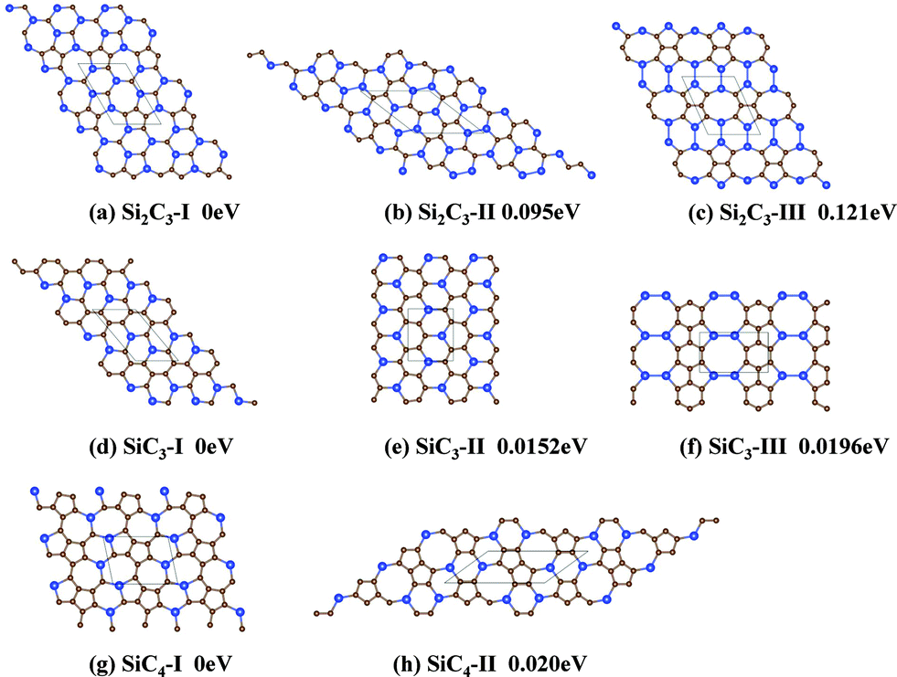 | ||
| Fig. 1 Predicted low-lying solid structures of 2D Si–C compounds based on the PSO simulations. C and Si atoms are represented by brown and blue spheres. The computed relative energy per atom with respect to the lowest-energy structure is given beneath each structure. | ||
To evaluate the relative stabilities among the predicted 2D C–Si compounds, we have computed their cohesive energy. The formula of cohesive energy for the 2D systems is defined as follows:
| Ecoh = (xESi + yEC − ESixCy)/(x + y) |
| 2D Structure | Cohesive energy (eV per atom) |
|---|---|
| Si2C3-I | 7.2660 |
| Si2C3-II | 7.1712 |
| Si2C3-III | 7.1446 |
| SiC3-I | 7.8561 |
| SiC3-II | 7.8409 |
| SiC3-III | 7.8365 |
| SiC4-I | 8.0631 |
| SiC4-II | 8.0434 |
Next, to ensure that the predicted lowest-energy structure for each Si:C ratio is dynamically stable, phonon spectra of all of the three lowest-energy structures were computed using the supercell frozen phonon theory implemented in the PHONOPY program. The computed phonon spectra of the lowest-energy structures of Si2C3, SiC3 and SiC4 (Si2C3-I, SiC3-I and SiC4-I) are plotted in Fig. 2. Clearly, no negative phonon frequencies are present over the entire Brillouin zones for all three of the lowest-energy structures, indicating the inherent dynamical stability of these 2D Si–C sheets.
 | ||
| Fig. 2 Computed phonon band structures of (a) Si2C3-I, (b) SiC3-I and (c) SiC4-I. Γ(0.0, 0.0, 0.0), X(0.5, 0.0, 0.0), Y(0.0, 0.5, 0.0) and S(0.5, 0.5, 0.0) refer to special points in the first Brillouin zone. | ||
Moreover, the thermal stability of the Si2C3-I, SiC3-I and SiC4-I structures was examined using ab initio molecular dynamics (AIMD) simulations. In the AIMD simulation, the canonical ensemble (NVT ensemble) is adopted. The AIMD time step was 2 fs and the total simulation time was 15 ps for each given temperature. The structural features of each Si–C sheet prior to and after melting are shown in Fig. 3. It can be seen that the equilibrium structures of the Si2C3-I and SiC3-I sheets at the end of the 15 ps AIMD simulation show no sign of structural disruption at 3500 K, whereas both sheets exhibit disrupted structures at 4000 K. Thus we can conclude that the Si2C3-I and SiC3-I structures can maintain their structure integrity and planar geometry below 3500 K. The SiC4-I sheet appears to have the highest thermal stability among the three structures, as SiC4-I can still keep its geometric structure over the 15 ps AIMD simulation with the temperature controlled at 4000 K.
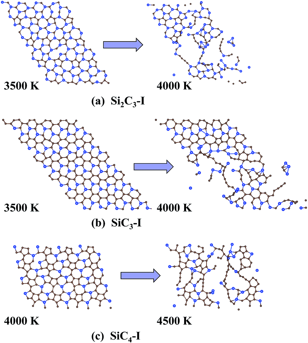 | ||
| Fig. 3 Snapshots of the three lowest-energy 2D Si–C compounds at the end of two independent 15 ps AIMD simulations: (a) Si2C3-I, (b) SiC3-I and (c) SiC4-I sheets. | ||
B. Detailed structures of the three 2D Si–C compounds
The Si2C3-II sheet is 94.8 meV per atom higher in energy than the Si2C3-I sheet, although all of the polygonal rings in the Si2C3-II sheet are hexagonal. Notably, this Si2C3-II sheet can be viewed as silicon-doped graphene. In contrast to the Si2C3-I sheet where all of the Si atoms are located separately (no Si–Si bonds were found in the sheet), there are both separately-distributed Si atoms and Si dimers in the Si2C3-II sheet. The percentage of Si atoms forming Si dimers is 50%. Since the sp2-hybridization is not favored by silicon Si–Si bonds, a planar structure should be energetically unfavorable, which is possibly a major reason why Si2C3-II is less stable than Si2C3-I.
The third lowest-energy structure of Si2C3, namely the Si2C3-III sheet, is 121.4 meV per atom higher in energy than the Si2C3-I sheet. Apparently, the Si2C3-III sheet is composed of pentagonal, hexagonal and octagonal rings, where each octagonal ring is surrounded by four pentagonal and four hexagonal rings. In this structure, all of the Si atoms form Si dimers so that its energy is much higher than that of the Si2C3-I or Si2C3-II sheet.
The structure of the SiC3-II sheet is also graphene like.41 The Si atoms in the SiC3-II sheet are also located separately, as in the SiC3-I sheet (see Fig. 1e). So, it is surprising that the SiC3-II sheet is 15.2 meV per atom higher in energy than the SiC3-I sheet. A closer examination of the structure indicates that the only difference between the structure of the SiC3-I and SiC3-II sheets is the location of the two Si atoms in every hexagonal ring. In the SiC3-I sheet, the two Si atoms are located at the 1 and 3 sites of every hexagonal ring (we denote the six sites of any hexagonal ring as site 1 to site 6), while in the SiC3-II sheet they are located at the 1 and 4 sites. From the viewpoint of doping, the SiC3-II sheet can be viewed as having 25% of the A-site and 25% of the B-site carbon atoms of the graphene substituted by Si atoms. The different location distribution of the Si atoms leads to more of the C atoms being connected with one another in the SiC3-I sheet compared to SiC3-II, which should be the main reason why the SiC3-I sheet has a lower energy than the SiC3-II sheet. Due to the different Si distributions, the structure of the SiC3-II sheet cannot be decomposed into C chains and Si–C chains, while that of the SiC3-I sheet can.
The structure of the SiC3-III sheet is very different from those of the SiC3-I and SiC3-II sheets (see Fig. 1f). The SiC3-III sheet is composed of octagonal, hexagonal, and pentagonal rings, and possesses a much higher symmetry compared to the SiC3-I and SiC3-II sheets. The Si atoms in the SiC3-III sheet form dimers while the C atoms form complete hexagonal rings. It is known that Si dimers in a planar structure are energetically not favored whereas C hexagonal rings are favored. So, even though Si–Si bonds exist, the total energy of the SiC3-III sheet is only a little higher than that of SiC3-II sheet.
Finally, we make a comparison of the C–C/C–Si bond length in graphene/SiC and the SiC compounds reported here. The C–C bond lengths in Si2C3-I, SiC3-I, and SiC4-I are 1.438 Å, 1.455 Å, and 1.432 Å respectively, slightly longer than that in graphene (1.42 Å). The C–Si bonds are slightly longer in Si2C3-I (1.792 Å) than those either in the SiC sheet (1.786 Å), or in SiC3-I (1.781 Å) and SiC4-I (1.770 Å). We have also computed the Si–Si distance between two parallel stacked (in registry) Si2C3-I monolayers. As shown in ESI Fig. S1,† the minimum Si–Si distance is about 3.4 Å. Hence, new Si–Si bonds are not expected to form when two Si2C3-I monolayers are stacked on top of one another.
In summary, although the 2D Si–C compounds considered here are all C-rich, most of the lowest-energy structures and low-energy metastable structures are not akin to Si-doped graphene. Pentagonal and heptagonal rings are occasionally formed in the lowest-energy structures, and octagonal rings normally appear in the metastable structures. The Si atoms tend to be located separated from one another, i.e. the Si atoms prefer to be bonded with C atoms but not Si atoms, which is a main factor that influences the relative stability of the 2D Si–C structures.
C. Electronic properties of 2D Si–C compounds
The computed electronic band structures of the Si2C3-I, SiC3-I and SiC4-I sheets, based on GGA calculations, are plotted in Fig. 4. It can be seen that all three of the lowest-energy structures are semiconducting, among which the Si2C3-I and SiC3-I sheets possess a direct bandgap, while the SiC4-I sheet exhibits an indirect bandgap. The computed bandgaps of the Si2C3-I, SiC3-I and SiC4-I sheets (at GGA level) are 0.83 eV, 0.86 eV and 0.14 eV, respectively (see Table 2), and all belong to the narrow-gap semiconductors. Note that GGA calculations tend to underestimate the bandgaps of semiconducting materials. To predict the bandgap of each Si–C compound more accurately, we also performed band-structure calculations using the HSE0642–44 functional which has been proven to be more accurate for bandgap computation. The bandgaps of the Si2C3-I, SiC3-I and SiC4-I sheets (based on HSE06 calculations) are 1.37 eV, 1.40 eV, and 0.51 eV, respectively. The bandgaps of the Si2C3-I and SiC3-I sheets are very close to that of bulk silicon, while the bandgap of the SiC4-I sheet is close to that of bulk germanium. Like bulk silicon and germanium, these 2D Si–C compounds may find applications in nanoelectronic devices. | ||
| Fig. 4 Computed electronic band structures of (a) Si2C3-I, (b) SiC3-I and (c) SiC4-I monolayer sheets. The Fermi level is set to 0 eV. | ||
| 2D Structure | Bandgap | |
|---|---|---|
| GGA | HSE06 | |
| Si2C3-I | 0.83 eV (D) | 1.37 eV (D) |
| SiC3-I | 0.86 eV (D) | 1.40 eV (D) |
| SiC4-I | 0.14 eV (I) | 0.51 eV (I) |
The computed partial density of states (PDOSs) of the predicted 2D Si–C compounds was also analyzed. The representative PDOSs for Si2C3-I, SiC3-I and SiC4-I sheets are plotted in Fig. 5. It is clear that in all three cases the higher valence bands and lower conduction bands (about −2.0 to 2.5 eV of the energy windows) are contributed by the sp2 orbitals of Si and C, while the pz orbitals of Si and C only have contributions to the lower valence bands (below −2.0 eV) and higher conduction bands. So, the electronic properties of these sheets are only determined by the in-plane σ and σ* bonds rather than the π and π* states, in contrast to graphene and graphite where the conjugate π states have a major influence on the electronic properties such as excellent conductivity.
 | ||
| Fig. 5 Computed PDOSs for (a) Si2C3-I, (b) SiC3-I and (c) SiC4-I monolayer sheets. The Fermi level is set at 0 eV. | ||
For the Si2C3-I sheet, it is clearly shown that the valence band maximum (VBM) is mainly contributed by the s, px and py orbitals of the C atoms, while the contribution of Si is about half that of C. On the other hand, the conduction band minimum (CBM) is mainly contributed by Si atoms and the contribution of C atoms is about half that of Si. For the SiC3-I sheet, both the VBM and CBM are contributed mainly by the sp2 hybridization states of C. And for the SiC4-I sheet, it is obvious that the C and Si atoms contribute to the VBM and CBM nearly equally. It is worth noting that there are such large differences in the contribution to the VBM and CBM states for different 2D Si–C compounds.
To gain a deeper understanding of the nature of the bonding for the predicted 2D Si–C compounds, we applied the electron localization function (ELF) analysis, which can be used to classify chemical bonds rigorously. Due to the more localized characteristic of σ states than π states, a relatively large value of ELF distribution (e.g., 0.725) for the Si–C compounds can mostly characterize the in-plane σ states. The plotted iso-surfaces of ELFs for the lowest-energy Si–C sheets are shown in Fig. 6. It can be seen that in all the cases the ELFs of the C–C bonds are localized just at the center of the bonds and those of the Si–C bonds are localized closer to the C atoms. This is due to the fact that the electronegativity of the C atoms is stronger than that of the Si atoms. For the Si2C3-I sheet, apparently there are more Si–C bonds. The incline of ELFs to the C atoms suggests that both the VBM and CBM states mainly originate from the in-plane sp2 hybridization states of C and Si, respectively. For the other two cases, most of the C atoms connect with one another, forming C chains. The composition of Si–C bonds in SiC3-I and SiC4-I sheets are lower than that in the Si2C3-I sheet, hence the charge transfer from Si to C is weaker as reflected by the fact that the contribution of the Si sp2 states to the VBM is minor in both cases.
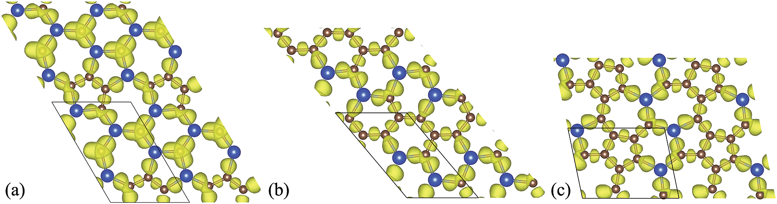 | ||
| Fig. 6 Iso-surfaces of the ELF with the value of 0.725 for (a) Si2C3-I, (b) SiC3-I and (c) SiC4-I sheets. | ||
D. Elastic properties of Si–C sheets
As mentioned above, the predicted lowest-energy structures of Si2C3, SiC3 and SiC4 sheets all possess excellent semiconducting properties that may be exploited for nanoelectronic applications. To this end, the mechanic strengths of the Si–C sheets are also important. It is well known that graphene possesses excellent elastic properties with large elastic constants: c11 = 906.70 GPa and c12 = 244.50 GPa. Previous studies have shown that silicene also has good elastic properties (c11 = 287 GPa and c12 = 127 GPa). We thus speculate that the predicted Si–C sheets may also possess good elastic properties. Based on density functional theory calculations, elastic constants of these 2D Si–C compounds were computed (see Table 3). To evaluate the specific value of elastic constants, we need to define interlayer spacing between two stacked SixCy sheets. Here, we estimate it to be ∼3.80 Å, which can be viewed as the thickness of a corresponding SixCy bilayer. Since the interlayer interaction is van der Waals like, akin to that in graphite, this interlayer distance is just an estimated value due to the limitation of DFT methods in describing weak interactions. Four important elastic constants c11, c12, c22 and c66 of the three lowest-energy Si–C sheets were computed based on GGA. One can see that the computed c11 and c12 of the Si–C sheets are between those of graphene and silicene, and both tend to increase with the concentration of C atoms in the Si–C sheets. Hence, the SiC4-I sheet possesses the largest value of c11 and c12 among the three Si–C sheets. However, a similar trend is not seen for c22 and c66. The computed c22 and c66 of the SiC3-I sheet are larger than those of the Si2C3-I and SiC4-I sheets. Overall, the predicted high elastic constants indicate that the 2D Si–C compounds possess reasonably good elastic properties.| 2D Structure | Elastic constants (GPa) | |||
|---|---|---|---|---|
| c 11 | c 12 | c 22 | c 66 | |
| Si2C3-I | 453.8 | 171.0 | 473.6 | 160.2 |
| SiC3-I | 594.5 | 180.8 | 640.2 | 231.5 |
| SiC4-I | 629.4 | 192.9 | 584.6 | 197.4 |
Conclusion
In conclusion, monolayer silicon–carbon (Si–C) materials can be viewed as composition-tunable materials between the pure 2D carbon monolayer – graphene – and the pure 2D silicon monolayer – silicene. Based on the PSO algorithm combined with density functional theory optimization, we performed an extensive 2D-crystalline search of monolayer structures of silicon–carbon compounds. A number of low-energy structures are predicted for different stoichiometric compositions (i.e., Si2C3, SiC3 and SiC4). In the most stable structures, each Si atom is bonded with three C atoms, favoring the sp2 hybridization. Dynamic and thermal stabilities of the predicted lowest-energy structures were examined through calculations of phonon dispersion and ab initio molecular dynamics simulations. These 2D Si–C compounds possess high thermal stabilities such that the Si2C3-I and SiC3-I sheets can retain their planar geometries below 3500 K while the SiC4-I sheet can even maintain its planar structure up to 4000 K. Next, the electronic and elastic properties of these three stable sheets were computed. Our calculations suggest that all of the predicted lowest-energy Si–C sheets are semiconductors with a moderate bandgap ranging from 0.5–1.5 eV, comparable to that of bulk silicon or germanium. Lastly, we found that these Si–C sheets possess reasonably high elastic constants whose values are typically between those of graphene and silicene. The composition dependent electronic and mechanical properties of 2D Si–C compounds may find applications in nanoelectronic devices.Acknowledgements
RLZ thanks the support of the National Natural Science Foundation of China (Grant no. 11104056), the Natural Science Foundation of Anhui Province (Grant no. 11040606Q33). XCZ is supported by ARL (Grant no. W911NF1020099), NSF (Grant no. DMR-0820521), and a grant from USTC for (1000 Talents Program) Qianren-B summer research.References
- K. S. Novoselov, A. K. Geim, S. V. Morozov, D. Jiang, Y. Zhang, S. V. Dubonos, I. V. Grigorieva and A. A. Firsov, Science, 2004, 306, 666 CrossRef CAS PubMed.
- K. S. Novoselov, A. K. Geim, S. V. Morozov, D. Jiang, M. I. Katsnelson, I. V. Grigorieva, S. V. Dubonos and A. A. Firsov, Nature, 2005, 438, 197 CrossRef CAS PubMed.
- K. S. Novoselov, E. McCann, S. V. Morozov, V. I. Falko, M. I. Katsnelson, U. Zeitler, D. Jiang, F. Schedin and A. K. Geim, Nat. Phys., 2006, 2, 177 CrossRef.
- Y. B. Zhang, Y. W. Tan, H. L. Stormer and P. Kim, Nature, 2005, 438, 201 CrossRef CAS PubMed.
- Q. Tang, Z. Zhou and Z. Chen, Nanoscale, 2013, 5, 4541 RSC.
- A. Fleurence, R. Friedlein, T. Ozaki, H. Kawai, Y. Wang and Y. Yamada-Takamura, Phys. Rev. Lett., 2012, 108, 245501 CrossRef.
- B. Feng, Z. Ding, S. Meng, Y. Yao, X. He, P. Cheng, L. Chen and K. Wu, Nano Lett., 2012, 12, 3507 CrossRef CAS PubMed.
- S. Y. Zhou, G. H. Gweon, A. V. Fedorov, P. N. First, W. A. de Heer, D. H. Lee, F. Guinea, A. H. Castro Neto and A. Lanzara, Nat. Mater., 2007, 6, 770 CrossRef CAS PubMed.
- L. Yang, C. H. Park, Y. W. Son, M. L. Cohen and S. G. Louie, Phys. Rev. Lett., 2007, 99, 186801 CrossRef.
- H. J. Xiang, B. Huang, Z. Y. Li, S. H. Wei, J. L. Yang and X. G. Gong, Phys. Rev. X, 2012, 2, 011003 Search PubMed.
- Z. Ni, Q. Liu, K. Tang, J. Zheng, J. Zhou, R. Qin, Z. Gao, D. Yu and J. Lu, Nano Lett., 2012, 12, 113 CrossRef CAS PubMed.
- S. Lebègue, M. Klintenberg, O. Eriksson and M. I. Katsnelson, Phys. Rev. B: Condens. Matter Mater. Phys., 2009, 79, 245117 CrossRef.
- J. N. Coleman, M. Lotya, A. O. Neill, S. D. Bergin, P. J. King, U. Khan, K. Young, A. Gaucher, S. De, R. J. Smith, I. V. Shvets, S. K. Arora, G. Stanton, H.-Y. Kim, K. Lee, G. T. Kim, G. S. Duesberg, T. Hallam, J. J. Boland, J. J. Wang, J. F. Donegan, J. C. Grunlan, G. Moriarty, A. Shmeliov, R. J. Nicholls, J. M. Perkins, E. M. Grieveson, K. Theuwissen, D. W. McComb, P. D. Nellist and V. Nicolosi, Science, 2011, 331, 568 CrossRef CAS PubMed.
- J. Feng, X. Sun, C. Wu, L. Peng, C. Lin, S. Hu, J. Yang and Y. Xie, J. Am. Chem. Soc., 2011, 133, 17832 CrossRef CAS PubMed.
- J. Feng, L. Peng, C. Wu, X. Sun, S. Hu, C. Lin, J. Dai, J. Yang and Y. Xie, Adv. Mater., 2012, 24, 1969 CrossRef CAS PubMed.
- Y. Sun, H. Cheng, S. Gao, Z. Sun, Q. Liu, F. Lei, T. Yao, J. He and S. Wei, et al. , Angew. Chem., Int. Ed., 2012, 51, 8727 CrossRef CAS PubMed.
- X. Yu, L. Li, X. W. Xu and C. C. Tang, J. Phys. Chem. C, 2012, 116, 20075 CAS.
- X. Wu, J. Dai, Y. Zhao, Z. Zhuo, J. Yang and X. C. Zeng, ACS Nano, 2012, 6, 7443 CrossRef CAS PubMed.
- X. J. Wu, Y. Pei and X. C. Zeng, Nano Lett., 2009, 9, 1577 CrossRef CAS PubMed.
- X. Luo, J. Yang, H. Liu, X. Wu, Y. Wang, Y. Ma, S. H. Wei, X. Gong and H. Xiang, J. Am. Chem. Soc., 2011, 133, 16285 CrossRef CAS PubMed.
- J. Dai, Y. Zhao, X. J. Wu, J. L. Yang and X. C. Zeng, J. Phys. Chem. Lett., 2013, 4, 561 CrossRef CAS.
- J. Dai, X. J. Wu, J. L. Yang and X. C. Zeng, J. Phys. Chem. Lett., 2014, 5, 2058 CrossRef CAS.
- H. J. Xiang, B. Huang, Z. Y. Li, S. H. Wei, J. L. Yang and X. G. Gong, Phys. Rev. X, 2012, 2, 011003 Search PubMed.
- Z. Ni, Q. Liu, K. Tang, J. Zheng, J. Zhou, R. Qin, Z. Gao, D. Yu and J. Lu, Nano Lett., 2012, 12, 113 CrossRef CAS PubMed.
- A. O'Hare, F. V. Kusmartsev and K. I. Kugel, Nano Lett., 2012, 12, 1045 CrossRef PubMed.
- Z. Zhang, X. Liu, B. I. Yakobson and W. Guo, J. Am. Chem. Soc., 2012, 134, 19326 CrossRef CAS PubMed.
- H. Sahin, S. Cahangirov, M. Topsakal, E. Bekaroglu, E. Akturk, R. Senger and S. Ciraci, Phys. Rev. B: Condens. Matter Mater. Phys., 2009, 80, 155453 CrossRef.
- C. Freeman, F. Claeyssens, N. Allan and J. Harding, Phys. Rev. Lett., 2006, 96, 066102 CrossRef.
- Y. Li, F. Li, Z. Zhou and Z. Chen, J. Am. Chem. Soc., 2011, 133, 900 CrossRef CAS PubMed.
- L. Zhou, Y. Zhang and L. Wu, Nano Lett., 2013, 13, 5431 CrossRef CAS PubMed.
- Y. C. Wang, J. Lv, L. Zhu and Y. M. Ma, Phys. Rev. B: Condens. Matter Mater. Phys., 2010, 82, 094116 CrossRef.
- Y. Ma, M. I. Eremets, A. R. Oganov, Y. Xie, I. Trojan, S. Medvedev, A. O. Lyakhov, M. Valle and V. Prakapenka, Nature, 2009, 458, 182 CrossRef CAS PubMed.
- A. R. Oganov, Y. M. Ma, Y. Xu, I. Errea, A. Bergara and A. O. Lyakhov, Proc. Natl. Acad. Sci. U. S. A., 2010, 107, 7646 CrossRef CAS PubMed.
- Y. Xie, A. R. Oganov and Y. Ma, Phys. Rev. Lett., 2010, 104, 177005 CrossRef.
- R. L. Zhou and X. C. Zeng, J. Am. Chem. Soc., 2012, 134, 7530 CrossRef CAS PubMed.
- R. Zhou, B. Qu, J. Dai and X. C. Zeng, Phys. Rev. X, 2014, 4, 011030 Search PubMed.
- J. Dai, X. J. Wu, J. L. Yang and X. C. Zeng, J. Phys. Chem. Lett., 2013, 4, 3484 CrossRef CAS.
- G. Kresse and J. Furthmüller, Phys. Rev. B: Condens. Matter Mater. Phys., 1996, 54, 11169 CrossRef CAS.
- A. Togo, F. Oba and I. Tanaka, Phys. Rev. B: Condens. Matter Mater. Phys., 2008, 78, 134106 CrossRef.
- Y. Ding and Y. Wang, J. Phys. Chem. C, 2014, 118, 4509 CAS.
- Q. Tang and Z. Zhou, Prog. Mater. Sci., 2013, 58, 1244 CrossRef CAS PubMed.
- J. Heyd, G. E. Scuseria and M. Ernzerhof, J. Chem. Phys., 2003, 118, 8207 CrossRef CAS PubMed.
- J. Heyd, G. E. Scuseria and M. Ernzerhof, J. Chem. Phys., 2006, 124, 219906 CrossRef PubMed.
- J. Heyd and G. E. Scuseria, J. Chem. Phys., 2004, 121, 1187 CrossRef CAS PubMed.
Footnote |
| † Electronic supplementary information (ESI) available. See DOI: 10.1039/c4nr03247k |
| This journal is © The Royal Society of Chemistry 2014 |