
 Open Access Article
 This Open Access Article is licensed under a Creative Commons Attribution-Non Commercial 3.0 Unported Licence
Anomalous behavior of nearly-entire visible band manipulated with degenerated image dipole array†
Lei
Zhang
a,
Jiaming
Hao
b,
Min
Qiu
c,
Said
Zouhdi
d,
Joel Kwang Wei
Yang
ef and
Cheng-Wei
Qiu
*a
aDepartment of Electrical and Computer Engineering, National University of Singapore, Singapore 117583, Singapore. E-mail: eleqc@nus.edu.sg
bNational Laboratory for Infrared Physics, Shanghai Institute of Technical Physics, Chinese Academy of Science, Shanghai 200083, China
cState Key Laboratory of Modern Optical Instrumentation, Department of Optical Engineering, Zhejiang University, Hangzhou 310027, China
dLaboratoire de Génie Electrique de Paris, Paris-Sud University, France
eInstitute of Materials Research and Engineering, A*STAR (Agency for Science, Technology and Research), 3 Research Link, 117602, Singapore
fEngineering Product Development, Singapore University of Technology and Design, 20 Dover Drive, Singapore 138682
First published on 7th August 2014
Abstract
Recently, the control of anomalous light bending via flat gradient-phase metasurfaces has enabled many unprecedented applications. However, either low manipulation efficiency or challenging difficulties in fabrication hinders their practical applications, in particular in the visible range. Therefore, a concept of degenerated image dipole array is reported to realize anomalous light bending with high efficiency. A continuous phase delay varying rather than a discrete one, along with an in-plane wave vector is utilized to achieve anomalous light bending, by controlling and manipulating the mutual coupling between dipole array and the dipole array of its image. The anomalous light bending covers almost the entire visible range with broad incident angles, accompanied with preserved well-defined planar wavefront. In addition, this design is feasible to be fabricated with recent nanofabrication techniques due to its planarized surface configuration. The concept of imperfect image dipole array degenerated from ideal metamaterial absorbers surprisingly empowers significant enhancement in light manipulation efficiency for visible light in a distinct fashion.
Introduction
Since the first lens was invented, manipulation of light in a desired manner has aroused significant interest especially in current nanophotonic devices. By designing the phase profile, arbitrary spatial distribution of light can be generated. Based on the principle of phase continuity at interface between two materials, conventional optical elements, such as lenses, gradient-index materials, gratings, etc., are used to control phase distribution by shaping the geometric or refractive index profile at the interfacial boundary.1 Thereafter, propagation properties of light can be modified accordingly. However, since the phase variation relies on the light propagation path, it is hard to provide sufficient phase control because of the limited permittivity and permeability of natural materials when the path size is reduced to micro- or even to nano-scale in current photonic devices. As a highly significant invention, metamaterials provide more freedom in controlling light since they can be designed to have arbitrary permittivity and permeability. Through tailoring the geometry or materials of components, many unusual phenomena have been demonstrated, such as subwavelength imaging,2 beam rotator,3 and invisibility cloaks.4,5 However, due to the bulk properties of metamaterials, recent nanofabrication techniques, such as electron-beam lithography and focused-ion beam impose a challenge in its applications at visible range.In recent works, by introducing an abrupt phase discontinuity at the surface of plasmonic structure, extraordinary light manipulation abilities have been demonstrated by two-dimensional (2D) ultrathin metamaterials,6,7 such as focusing,8,9 quarter-wave plate,10,11 vortex beam generation,6,12etc. Significant achievements lead to more flexibility in nanophotonic devices. However, there are still some unsolved issues hindering their practical applications. For example, through exciting the localized modes with different symmetries by a linear polarized light, a V-shape antenna array supports anomalous refraction/reflection due to interaction between these two kinds of modes at the near- and far-infrared ranges.6,7 Immediately, this anomalous phenomenon was extended to circular polarized light with orientated rectangular nanorod arrays.12 However, for both designs, light manipulation only occurs between opposite polarizations. Moreover, due to this cross-polarization effect, the manipulation efficiencies of these designs are quite low. In order to improve the efficiency and avoid polarization conversion, another type of metasurface based on an insulator, sandwiched by a layer of metallic nanorod arrays and a thick metal film was demonstrated to bend reflected light along a prescribed direction by inducing a magnetic resonance.13
More recently, a new type of multilayer structure was used to manipulate transmission at microwave range based on Huygens’ principle.14 Both electric and magnetic polarization currents were introduced to achieve a full control with high efficiency. In principle, the function of Huygens’ surface can be extended to manipulate the entire electromagnetic spectrum. However, since the necessary electric and magnetic currents should be provided by two separated layers with different designs along the incident wave vector, a considerable thickness was set by dimension and gaps between different layers. On the other hand, practical limitations in the current nanolithography fabrication techniques impose challenging restrictions on its realization at visible range due to the need of high accuracy in geometric dimensions and alignment of multiple stacks. In addition, at optical range, weak magnetic response degrades the phase response.15 Therefore, another type of meta-transmit-array was proposed and numerically demonstrated at mid-infrared range by using a stack of composite metascreen. By matching the impedance of proposed structure with environment, anomalous transmission was achieved efficiently.16 However, when realistic intrinsic loss was taken into account, the manipulation efficiency decreased considerably due to impedance mismatch caused by the increased imaginary part of permittivity especially at visible range. In addition, the same challenges in fabrication still exist owing to its stacking design and vertical gaps along the incident wave vector. Those challenges particularly at visible range motivated us to propose a single flat surface so that nanoparticles can be easily deposited by lithographic methods while high efficiency is retained in manipulating anomalous transmission.
Results and discussion
In this work, to overcome the abovementioned limitations, an ultrathin plasmonic nanostructure is reported to manipulate light at visible range only by using identical trapezoids to mimic a degenerated image dipole array. The underlying mechanism can be intuitively interpreted by using a simple image model. Due to the moderate thickness of middle continuous layer, the coupling between original dipoles and their induced imperfect image facilitates a convenient way in manipulating the phase and amplitude of refracted and reflected lights. Not only a broad range of phase delay but also an efficient amplitude control can be achieved by tuning the dimension sizes of the middle layer and nanoparticle. An optimized thickness of middle layer is helpful in realizing a uniform amplitude control with high efficiency. Whereas, geometry-dependent resonance is capable of imparting arbitrary phase delay into both refracted and reflected lights. Differing from conventional blazed grating, for example, with triangular grooves, it generates a constant phase gradient by varying the depth of groove within the incident plane. Our design could be regarded as a meta-blazed grating except that the phase delay is controlled by a geometry change perpendicular to the incident plane, which is promising in the applications of ultrathin devices. In comparing with previous V-shape and nanorod designs, our proposed structure not only supports a broadband anomalous control of refracted and reflected light, but also improves the manipulation efficiency higher by one order. Although the anomalous refracted efficiency supported by metascreen was claimed to be as high as 75% when intrinsic loss was very low, it drops lower than 40% once the realistic loss was considered in calculation.16 In addition, such a metascreen may meet critical challenges as the wavelength decreases to the visible range because the smallest size feature will be less than 3 nm and realistic loss of metal has to be considered. Since the specific size within each layer must be designed separately, the difficulty of that approach in practical applications significantly increases particularly at visible range. In this connection, our proposed method is able to provide a viable solution to this challenge in visible light with a competitive efficiency.As a proof-of-concept, light bending of both refracted and reflected light is numerically realized by periodically aligning trapezoids at the top and bottom of the central continuous layers. Our design only relies on the identical shape instead of the rotating elements of varying shapes. Because of its planar design and linear size changes, our design presents superior advantages in the fabrication aspect. Moreover, the central continuous layers with the thickness of tens of nanometres can be readily achieved with current deposition techniques. The bending angle can be exactly predicted with a modified diffraction equation. In comparison with previous works, our results significantly show that, even though without covering the 2π phase delay range or providing a constant phase gradient, light bending with high efficiency can be realized without a cross-polarization effect. Simultaneously, it should be noticed that a well-defined planar wavefront is also retained. Therefore, with the simplification in the phase requirements as well as improvement in manipulation performance, i.e. high efficiency and planar wavefront, the proposed degenerated image dipole array thus may empower a wide spectrum of interesting applications such as beam splitter,17 holography,18,19 beam guiding.20–23
Fig. 1a and b show the schematics of the design. The proposed structure is symmetric along the z-axis. Either the upper or lower half can work as a perfect absorber if the continuous Ag layer is thick enough to block the transmission. In that situation, the reflection is determined by the interference between radiations from the original electric dipole p and its image dipole p′ = (1 − εeff)/(1 + εeff)p shown in Fig. 1c. εeff represents the effective permittivity determined by Al2O3/Ag/Al2O3 layer and resonant mode. Their phase difference consists of two parts, ϕdelay and ϕs. The former one arises from excitation delay of p′ and the latter one from optical path length keff × s, where  is the effective wave vector and s is the difference in path length. When they have opposite phases at resonance wavelength λ0 by tuning their separation with dielectric layer, a destructive interference gives rise to a perfect absorption by eliminating reflection.24–26 Due to the resonance wavelength being mainly dependent on the thickness of dielectric layer, this kind of design has been demonstrated as a perfect absorber at a broadband range, with an optimized thickness.26–29 However, if the thickness of Ag layer is thinner than the penetration depth of metal, a part of the energy is able to pass through it. When a symmetric half is added at the bottom, another pair of dipoles is accordingly induced. Additional phase delay imparted to the induced dipole and its image makes them interfering in-phase in the transmission direction. As discussed in our previous paper,30,31 both symmetric and antisymmetric transverse modes coexist in the proposed structure. By tailoring the thickness of the continuous layer Al2O3, two modes can combine together to form a robust broadband transparency at visible range (brown, red and blue dashed lines shown in Fig. 1d). Because of the introduction of resonant modes, the transmittance is higher than their counterparts, supported by an Ag film with thickness of 20 nm (green solid line shown in Fig. 1d), and of the half proposed structure along the longitudinal direction (solid black line shown in Fig. 1d). After optimization, the thickness of Al2O3 layer is fixed at 30 nm in the following investigations. In addition, it should be emphasized that the continuous Ag layer plays a significant role in improving the performance of anomalous refraction and reflection. In addition, it helps in tuning the coupling strength between the top and bottom particles. Moreover, Ag film with moderate thickness is better to block unexpected direct transmission. A thicker Ag layer will block all the transmissions due to weak coupling strength, whereas a thinner or even no Ag layer will result in more unexpected transmission and a worse wavefront. In addition, without the continuous Ag layer, a broad range of phase delay is inherently limited by the three-layer structure (i.e. Ag particle/dielectric/Ag particle).32
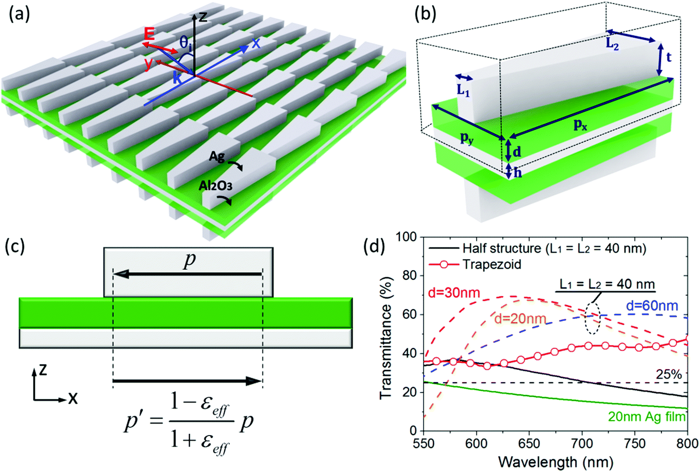 | ||
| Fig. 1 (a) Schematic image of the proposed design for manipulating linearly polarized light in both refraction and reflection. (b) A unit cell and parameter definitions. (c) Schematics of dipole p and its image p′ of a half structure. (d) Transmittance versus wavelength for flat Ag film with thickness of 20 nm (green solid line), proposed structure with L1 = L2 = 40 nm (i.e. one-dimensional nanowire) and d = 20 nm (brown dashed line), 30 nm (red dashed line) and 60 nm (blue dashed line), upper-half structure (fenced by black dashed lines in (b)) with L1 = L2 = 40 nm and d = 30 nm (black solid line) and the proposed design for light bending with L1 = 5 nm and L2 = 100 nm, px = 1200 nm and d = 30 nm (red solid line with circles). Other parameters are set as py = 150 nm, h = 20 nm and t = 50 nm. Black dashed line at 25% represents the theoretical limitation of anomalous refraction with cross-polarization effect.16 | ||
Accompanied with the energy exchange, additional phase delay is naturally imparted to the transmitted light. By varying the geometric dimension of nanoparticles, the phase delay arising from resonant mode is also controllable. To explore the dependence of phase response on geometric size, one-dimensional (1D) nanowires are first simulated, i.e., L1 and L2 are set to be equal to L. A plane wave with electric field linearly polarized along y-axis is normally incident on the proposed structure. The phase delays at different wavelengths are calculated for nanowires with different widths by utilizing the finite-difference time-domain (FDTD) with the permittivities of Ag and Al2O3 taken from experimental data.33 By tuning the width of nanowire from 5 nm to 120 nm, the phase delay of refracted light is plotted in Fig. 2a at wavelengths of 600 nm, 700 nm and 800 nm. The cover range of phase delay is as large as 1.5π within a broad band, which thus empowers a promising approach in manipulating light.
 | ||
| Fig. 2 (a) Phase delay Φ of transmitted light versus width of one-dimensional nanowire at wavelength λ = 600 nm, 700 nm and 800 nm. Here h = 20 nm, d = 30 nm, t = 50 nm and py = 150 nm. L1 = L2 = L ranges from 5 nm to 120 nm. (b) Schematic phase profiles of conventional blazed grating (black line) and the proposed structure at 600 nm wavelength. Red and blue lines denote two types of phase profile, one covering less than 2π (py = 150 nm, L1 = 5 nm, and L2 = 120 nm) and the other covering full 2π (py = 200 nm, L1 = 5 nm, and L2 = 140 nm), respectively. | ||
As a demonstration of bending the propagation of plane wave, gradual phase delay along the x-axis is needed to compensate the momentum change caused by redirection. Instead of discrete nanorod arrays or oriented V-shape ones used in previous works, trapezoids are chosen as the building blocks and are periodically arranged by aligning their parallel edges along the polarization direction of incident light, i.e. y-axis as shown in Fig. 1a. Therefore, a phase delay Φ will vary as a function of x when incident light is polarized along the y-axis because different transverse resonances are excited at each width along the trapezoid. Therefore, an even broadband response covering almost the entire visible range arises from the combination of the resonate response of different cross sections of the trapezoid at different wavelengths (red solid line with circles shown in Fig. 1d).29–31 Although the light bending is demonstrated with trapezoids connecting with neighbours, the broadband response can also be achieved when a small gap exists between neighbouring trapezoids (not shown). The origin of such a broadband response is different from the one based on connected split ring resonators presented in the previous work, in which both magneto-inductive interaction and the exchange of conduction current are employed to extend the propagation length of magnetic plasmon at a broad infrared band.34 It is noticeable that the transmittance of the proposed structure consisting of trapezoids (red solid line with circles) is slightly lower than the counterpart supported by nanowires (brown, red and blue dashed lines shown in Fig. 1d). The decrease can be attributed to the wavelength shift caused by the varying width along the trapezoid. However, it is still higher than the theoretical upper limitation of anomalous refraction with cross-polarization effect (black dashed line shown in Fig. 1d).16 Moreover, such a sacrifice in transmittance is designed to control the phase delay of transmitted light.
In contrast to conventional blazed grating and 2D metamaterials,6,7 which provide a linear phase variation from 0 to 2π within one period shown as black line in Fig. 2b, the proposed structure provides a nonlinear phase variation because of its nonlinear dependence on geometry change. As schematically shown in Fig. 2b, two types of phase profile may be provided by varying the width along the direction of polarization with different ranges. The type depicted by the red line (nonlinear with less than 2π coverage) will be employed to demonstrate the light bending here while the bending performance of blue one (nonlinear but with 2π coverage) will be explained in ESI.† Notably, both a constant phase gradient and a sufficient coverage of 2π phase delay are absent in our design. It is indeed possible to design a linear phase response by selecting the width of nanostructures along the x-axis according to the phase response shown in Fig. 2a. However, we will exhibit below that light can still be bent to a prescribed direction while the non-constant phase gradient does not significantly decrease the manipulation performance. Whereas, it is beneficial for reducing the cost by selecting an appropriate particle size for a constant phase gradient. Moreover, due to the symmetry of the proposed structure along the z-axis, phase change can also be imparted to reflected light. As a result, reflected light will bent in a similar way. In order to predict the bending angle of this anomalous refraction and reflection, the modified diffraction equation with abrupt phase delay introduced by resonance can be expressed as follows:6,7,12
 | (1) |
 | (2) |
To verify our abovementioned discussion, full wave simulations are performed with the periodicity along x-axis px = 1200 nm while along y-axis py = 150 nm. Within one period, the width of trapezoid varies from L1 = 5 nm to L2 = 100 nm. The upper and lower halves are symmetric with d = 30 nm and t = 50 nm, and for continuous silver layer h = 20 nm thick. The entire proposed structure is ultrathin with thickness of only 180 nm. The simulation is first carried out for a normal incident plane wave with electric field polarizing along the y-axis. As indicated by the red open dot line shown in Fig. 1d, the proposed structure supports a total transmittance around 40%.
Fig. 3a and b exhibit the Ey component for λ = 600 nm and 700 nm at y = 0 plane, respectively, where the proposed structure situated at the center is fenced by dashed lines. The bending effect is certainly demonstrated for both refraction and reflection. It should be noted that the strong field below z = 200 nm consists of both reflected and incident fields. Because a relatively small phase delay occurs at the left end due to narrow width of particle, while a large one occurs at the right end, the refracted or reflected field then deflects to the wider end of nanoparticle. The wavefront retains a well-defined planar form. The propagation angle can thus be estimated from the wavefront. For example, in Fig. 3a for λ = 600 nm, refraction θt and reflection θr angles are estimated to be 30.1° and 28.8°, respectively, which exactly match with the theoretically predicted angle 30°. We also simulated the Ey components when incidence is at 15°, as shown in Fig. 3c and d. The good planar wave feature is still retained with a well-defined propagation direction angle of 50.6° at λ = 600 nm, which agrees with the predicted 49.3° as well. It should be noted that the strong reflection is mainly caused by the significant intrinsic loss of noble metal at visible range, which leads to the impedance mismatch with free space. The intrinsic loss will also diminish the anomalous manipulation efficiency.16 In fact, the inherent problem is one of the most important factors hindering the practical applications of plasmonic structures. At visible range, the well-defined material properties of commonly used materials, such as silver, gold and aluminium, create difficulties to reduce the loss except for that new materials being used, which is beyond the studies of this work. On the other hand, the wavefront of reflected light also shows a good planar profile, which implies that both reflection and refraction are capable of being manipulated with the same design. From another perspective, our design therefore promises a device with integrated functions.
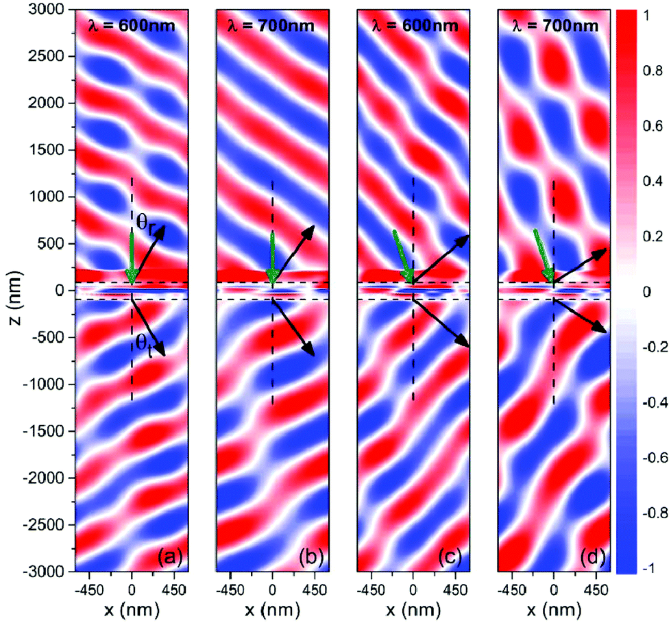 | ||
| Fig. 3 Electric field distributions of Ey component at wavelengths of 600 nm and 700 nm, based on the proposed structure with phase profile shown as red line in Fig. 2b. (a) and (b) are the field distributions with normally incident light. (c) and (d) are the field distributions with light of incident angle at 15°. Horizontal dashed lines represent the proposed structure located at the center. Dark green arrows represent the direction of incident light. | ||
In regards to diffraction theory, the diffraction angle is governed by the periodicity of the grating and is unaffected by the error in phase gradient.36 Thus, the anomalous bending angles still can be predicted with the theoretical equation even in the absence of a 2π phase accumulation and constant phase gradient. This can also be used, indeed, to conceptually interpret the anomalous bending angles of refraction and reflection in the works previously reported for light bending with metasurfaces.6,7,12 However, both deviations from full control requirements may cause side effect in the bending performance. Moreover, non-constant phase gradient may be a reason for generating an uneven wavefront as shown in Fig. 3. In addition, less than 2π coverage leads to a minor part of incident energy to be allocated to other unexpected orders. Once the efficiency of unexpected order is comparable to the anomalous one, the planar wavefront will get more difficult to be defined.
To further verify this point, we calculated the diffraction efficiency versus wavelength and refraction angle (Fig. 4a and b) or reflection angle (Fig. 4c and d). Dashed lines plotted in Fig. 4 are calculated with eqn (2), which match perfectly with the numerical results. Although other orders exist, the anomalous light mainly propagates along the m = +1 order, which is consistent with the simulated field distributions. In particular when other diffraction orders are totally suppressed, a near perfect planar wavefront can be obtained. As presented in Fig. 3b, the anomalous reflected light propagates as a perfect plane wave along 35.7° at λ = 700 nm for normal incidence. Usually the phase delay caused by resonance is wavelength-dependent, which will result in a dispersive light manipulation. As shown in Fig. 2, the giant phase delay almost covers the entire visible range. Therefore, the anomalous bending efficiencies are observed as high as 30% within a broadband ranging from 550 nm to 800 nm shown in Fig. 4, which is much higher than the theoretical limitation 25% of anomalous refraction with cross-polarization effect.16
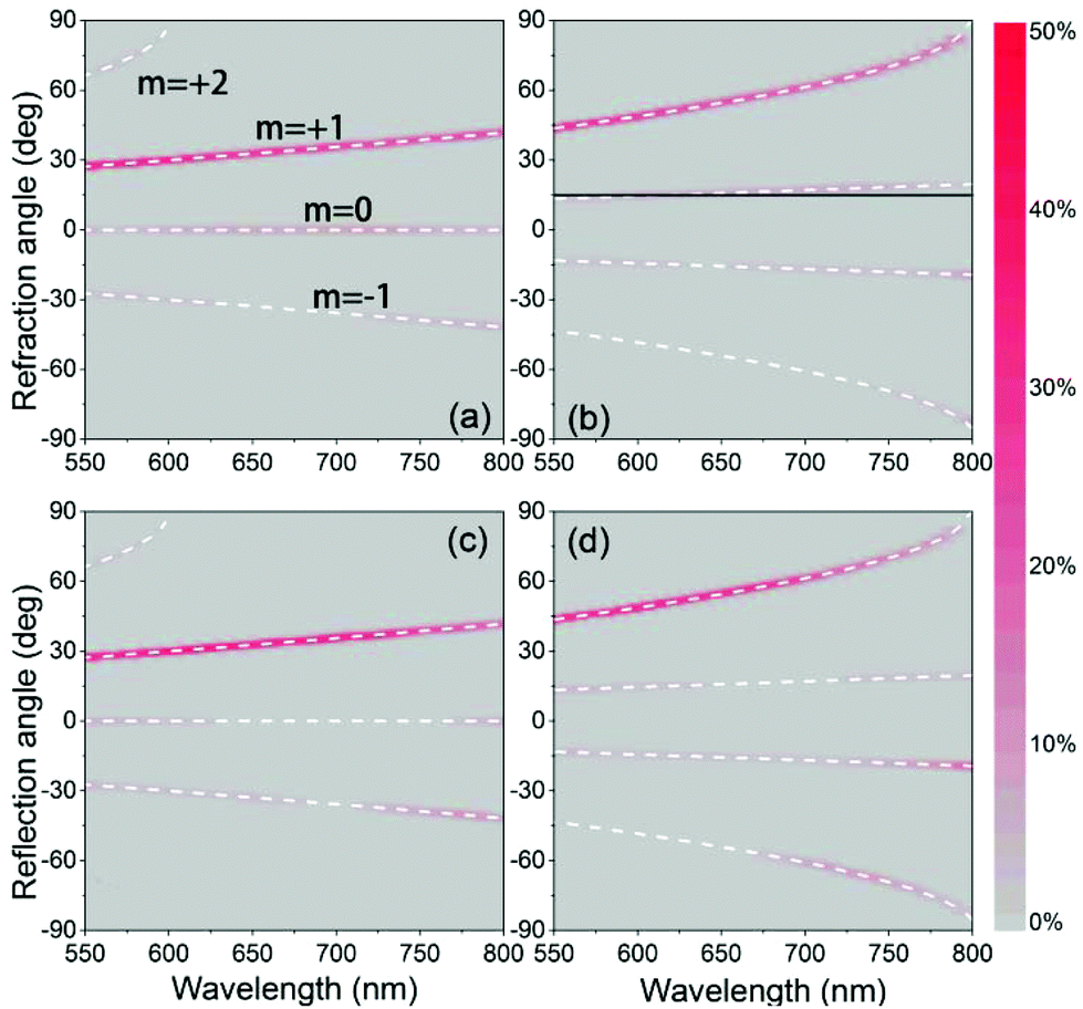 | ||
| Fig. 4 Investigation of bending efficiency versus refraction (a) and (b) or reflection angle (c) and (d) as well as wavelength at a fixed incident angle. (a) and (c) are calculated with normal incidence while (b) and (d) are calculated with incident angle around 15°. Gray solid line in (b) represents refraction angle 15° as a reference. White dashed lines shows the predicted angles, calculated with eqn (2). | ||
In addition to the broadband manipulation in both refraction and reflection, anomalous light bending is also supported within a broad angle range. In the simulation, to maintain a constant in-plane wave vector at all wavelengths, the actual incident angle changes as a function of wavelength at oblique incidence. Longer wavelengths will be injected at larger angles, while smaller wavelengths will be injected at smaller angles. With setting the incident angle at the center wavelength as 15°, the actual angle for Fig. 4b and d ranges from 13.4° to 19.7°, which can be recognized by m = 0 order labelled in Fig. 4b and d. The anomalous light bending for both refraction and reflection is obvious since most of the incident energy propagates along the direction defined by m = +1 order.
Conclusions
To conclude, we have proposed a novel, powerful solution to manipulate the propagation of electromagnetic waves at wavelength covering almost the entire visible range. Different from previous designs, our structure employs the coupling between the dipole and its imperfect image co-existing in both upper and lower halves. The resonant response of each half and their coupling in between can be easily modulated by tuning the thickness of the middle continuous layer and the width of nanoparticle. Therefore, a flexible method in spatially shaping both phase delay and amplitude can thus be achieved by simply tuning their geometric dimensions. In contrast to conventional blazed grating, which introduces phase delay with varying propagation path in the incident plane, the proposed meta-blazed grating introduces phase delay based on the excitation of a localized mode by tailoring the particle size along the direction perpendicular to the incident plane. For demonstration, by choosing trapezoids as the building blocks, incident light with linear polarization deflects to a prescribed direction and its bending angle is efficiently predicted with a modified diffraction equation. The planar wavefront of incident light was simultaneously well retained with high efficiency. Moreover, our result shows that even without fulfilment of proclaimed requirements in full control of electromagnetic wave, i.e., coverage of 2π phase delay and a constant phase gradient, light bending can still be achieved with good performance. In fact, in our case, it performs relatively better than the structure supporting 2π phase coverage in SI. The reduced requirement in light bending is significant for practical applications since 2π phase delay is not actually supported by usual resonances. Our work may realize versatile beam manipulations with sub-2π phase control. Moreover, the proposed design could be potentially applied in devices with integrated functions because both refraction and reflection can be manipulated within same design.Compared to previous works, our design not only improves the efficiency in light manipulation within a broad range of visible light and angle, but also alleviates the control requirements in light manipulation. Moreover, it is feasible to be realized with current nanofabrication techniques due to its planar design. Since the phase delay is polarization-dependent, the meta-blazed grating is also capable of sorting the polarization of incident light when both x- and y-polarized components are involved in incidence. For other applications, such as touch screens and LEDs, transparent conductive film (TCF) with high conductivity is significantly favourable. So far, indium tin oxide (ITO) is widely used at visible range, which has electrical resistance 800 ohm per square with thickness of 20 nm.37 However, the counterpart of Ag with similar thickness is only as small as 10 ohm per square,38 which may appear as a good candidate in TCF with integrated function for optical signal control. We believe the concept of the proposed broadband flat meta-blazed grating may lead to significant improvements in nanophotonic and optical devices especially in visible light, where considerable loss is inevitable.
Methods
The simulation of reflection/refraction spectra and field distributions were performed by means of LUMERICAL, a commercial finite-difference time-domain (FDTD) code. If there is no specific instruction, a plane wave polarized along the y-axis was used as incidence (see the definition of coordinates in Fig. 1a).Acknowledgements
This work was supported by grant R-263-000-A45-112 from National University of Singapore. J.H. acknowledges the support by Shanghai Pujiang Program (14PJ1409500).Notes and references
- M. Born and E. Wolf, Principles of Optics, Cambridge University Press, Cambridge, 7th edn, 1999 Search PubMed.
- J. B. Pendry, Phys. Rev. Lett., 2000, 85, 3966–3969 CrossRef CAS.
- H. Chen, B. Hou, S. Chen, X. Ao, W. Wen and C. T. Chan, Phys. Rev. Lett., 2009, 102, 183903 CrossRef.
- D. Schurig, J. J. Mock, B. J. Justice, S. A. Cummer, J. B. Pendry, A. F. Starr and D. R. Smith, Science, 2006, 314, 977–980 CrossRef CAS PubMed.
- Y. Liu and X. Zhang, Nanoscale, 2012, 4, 5277–5292 RSC.
- N. Yu, P. Genevet, M. A. Kats, F. Aieta, J.-P. Tetienne, F. Capasso and Z. Gaburro, Science, 2011, 334, 333–337 CrossRef CAS PubMed.
- X. Ni, N. K. Emani, A. V. Kildishev, A. Boltasseva and V. M. Shalaev, Science, 2012, 335, 427 CrossRef CAS PubMed.
- F. Aieta, P. Genevet, M. A. Kats, N. Yu, R. Blanchard, Z. Gaburro and F. Capasso, Nano Lett., 2012, 12, 4932–4936 CrossRef CAS PubMed.
- A. Pors, M. G. Nielsen, R. L. Eriksen and S. I. Bozhevolnyi, Nano Lett., 2013, 13, 829–834 CrossRef CAS PubMed.
- N. Yu, F. Aieta, P. Genevet, M. A. Kats, Z. Gaburro and F. Capasso, Nano Lett., 2012, 12, 6328–6333 CrossRef CAS PubMed.
- Y. Zhao and A. Alù, Nano Lett., 2013, 13, 1086–1091 CrossRef CAS PubMed.
- L. Huang, X. Chen, H. Mühlenbernd, G. Li, B. Bai, Q. Tan, G. Jin, T. Zentgraf and S. Zhang, Nano Lett., 2012, 12, 5750–5755 CrossRef CAS PubMed.
- S. Sun, K.-Y. Yang, C.-M. Wang, T.-K. Juan, W. T. Chen, C. Y. Liao, Q. He, S. Xiao, W.-T. Kung, G.-Y. Guo, L. Zhou and D. P. Tsai, Nano Lett., 2012, 12, 6223–6229 CrossRef CAS PubMed.
- C. Pfeiffer and A. Grbic, Phys. Rev. Lett., 2013, 110, 197401 CrossRef.
- R. Merlin, Proc. Natl. Acad. Sci. U. S. A., 2009, 106, 1693–1698 CrossRef CAS PubMed.
- F. Monticone, N. M. Estakhri and A. Alù, Phys. Rev. Lett., 2013, 110, 203903 CrossRef.
- J. S. Q. Liu, R. A. Pala, F. Afshinmanesh, W. Cai and M. L. Brongersma, Nat. Commun., 2011, 2, 525 CrossRef PubMed.
- S. Larouche, Y.-J. Tsai, T. Tyler, N. M. Jokerst and D. R. Smith, Nat. Mater., 2012, 11, 450–454 CrossRef CAS PubMed.
- M. Ozaki, J.-i. Kato and S. Kawata, Science, 2011, 332, 218–220 CrossRef CAS PubMed.
- R. Liu, Q. Cheng, J. Y. Chin, J. J. Mock, T. J. Cui and D. R. Smith, Opt. Express, 2009, 17, 21030–21041 CrossRef CAS PubMed.
- Y. Yang, A. Q. Liu, L. K. Chin, X. M. Zhang, D. P. Tsai, C. L. Lin, C. Lu, G. P. Wang and N. I. Zheludev, Nat. Commun., 2012, 3, 651 CrossRef CAS PubMed.
- J. Lin, J. P. B. Mueller, Q. Wang, G. H. Yuan, N. Antoniou, X. C. Yuan and F. Capasso, Science, 2013, 340, 331–334 CrossRef CAS PubMed.
- N. Yu, Q. Wang and F. Capasso, Laser Photonics Rev., 2012, 6, 24–46 CrossRef PubMed.
- A. Moreau, C. Ciraci, J. J. Mock, R. T. Hill, Q. Wang, B. J. Wiley, A. Chilkoti and D. R. Smith, Nature, 2012, 492, 86–89 CrossRef CAS PubMed.
- M. Albooyeh and C. R. Simovski, Opt. Express, 2012, 20, 21888–21895 CrossRef CAS PubMed.
- Z. H. Zhu, H. Liu, S. M. Wang, T. Li, J. X. Cao, W. M. Ye, X. D. Yuan and S. N. Zhu, Appl. Phys. Lett., 2009, 94, 103106 CrossRef PubMed.
- J. Hao, L. Zhou and M. Qiu, Phys. Rev. B: Condens. Matter, 2011, 83, 165107 CrossRef.
- C. Wu, N. Burton III, S. Gennady, J. Jeremy, M. Andrew, Z. Byron and S. Steve, Phys. Rev. B: Condens. Matter, 2011, 84, 075102 CrossRef.
- K. Aydin, V. E. Ferry, R. M. Briggs and H. A. Atwater, Nat. Commun., 2011, 2, 517 CrossRef PubMed.
- J. Hao, C.-W. Qiu, M. Qiu and S. Zouhdi, Opt. Lett., 2012, 37, 4955–4957 CrossRef CAS PubMed.
- L. Zhang, J. Hao, H. Ye, S. P. Yeo, M. Qiu, S. Zouhdi and C.-W. Qiu, Nanoscale, 2013, 5, 3373–3379 RSC.
- B. Memarzadeh and H. Mosallaei, Opt. Lett., 2011, 36, 3623–3623 CrossRef.
- E. D. Palik, Handbook of Optical Constants, Academic Press, San Diego, 1998 Search PubMed.
- H. Liu, D. A. Genov, D. M. Wu, Y. M. Liu, J. M. Steele, C. Sun, S. N. Zhu and X. Zhang, Phys. Rev. Lett., 2006, 97, 243902 CrossRef CAS.
- D. Zhaogang, B. Michel, Z. Di, G. Xiao Ming and K. W. Y. Joel, Nanotechnology, 2014, 25, 135303 CrossRef PubMed.
- S. Larouche and D. R. Smith, Opt. Lett., 2012, 37, 2391–2393 CrossRef PubMed.
- M. Mazur, D. Kaczmarek, J. Domaradzki, D. Wojcieszak, S. Song and F. Placido, Adv. Semicond. Devices Microsyst., 8th Int. Conf., 2010.
- V. J. Logeeswaran, N. P. Kobayashi, M. S. Islam, W. Wu, P. Chaturvedi, N. X. Fang, S. Y. Wang and R. S. Williams, Nano Lett., 2008, 9, 178–182 CrossRef PubMed.
Footnote |
| † Electronic supplementary information (ESI) available: The calculation of phase delay, the comparison of bending performance of the proposed structure with two types of phase profile shown in Fig. 2b, as well as a discussion of factors affecting the bending performance of the proposed design. See DOI: 10.1039/c4nr03163f |
| This journal is © The Royal Society of Chemistry 2014 |