
 Open Access Article
 This Open Access Article is licensed under a
 Creative Commons Attribution 3.0 Unported Licence
Driving forces for the self-assembly of graphene oxide on organic monolayers†
Johannes
Kirschner‡
a,
Zhenxing
Wang‡
a,
Siegfried
Eigler
bc,
Hans-Peter
Steinrück
d,
Christof M.
Jäger
e,
Timothy
Clark
e,
Andreas
Hirsch
bc and
Marcus
Halik
*a
aOrganic Materials & Devices (OMD), Institute of Polymer Materials, Friedrich-Alexander-University Erlangen-Nürnberg (FAU), Martensstraße 7, 91058 Erlangen, Germany. E-mail: marcus.halik@fau.de
bDepartment of Chemistry and Pharmacy, Friedrich-Alexander-University Erlangen-Nürnberg (FAU), Henkestraße 42, 91054 Erlangen, Germany
cInstitute of Advanced Materials and Processes (ZMP), Friedrich-Alexander-University Erlangen-Nürnberg (FAU), Dr.-Mack-Straße 81, 90762 Fürth, Germany
dInstitute of Physical Chemistry II and Interdisciplinary Center for Molecular Materials, Friedrich-Alexander-University Erlangen-Nürnberg (FAU), Egerlandstraße 3, 91058 Erlangen, Germany
eComputer Chemistry Center and Interdisciplinary Center for Molecular Materials, Friedrich-Alexander-University Erlangen-Nürnberg (FAU), Nägelsbachstraße 25, 91052 Erlangen, Germany
First published on 11th August 2014
Abstract
Graphene oxide (GO) flakes were self-assembled from solution on surfaces of self-assembled monolayers (SAMs), varying in the chemical structure of their head groups. The coverage density of GO relates to strength of attractive interaction, which is largest for Coulomb interaction provided by positively charged SAM head groups and negatively charged GO. A rough surface enhances the coverage density but with the same trend in driving force dependency. The self-assembly approach was used to fabricate field-effect transistors with reduced GO (rGO) as active layer. The SAMs as attractive layer for self-assembly remain almost unaffected by the reduction from GO to rGO and serve as ultra-thin gate dielectrics in devices, which operate at low voltages of maximum 3 V and exhibit a shift of the Dirac voltage related to the dipole moment of the SAMs.
Introduction
Graphene-based electronics have achieved remarkable progress during the last decade since the successful isolation of a monolayer from graphite.1,2 Due to the ultrahigh carrier mobility in the sp2 carbon network of graphene flakes, promising applications in high speed electronics and optoelectronics like frequency multipliers, mixers and photodetectors can be realized.3–7 They are also able to function on flexible substrates due to the outstanding mechanical properties of graphene.8,9 Although methods for producing large area graphene of high quality are available, the scalability of these methods is in need of improvement. In addition to that, the graphene films produced by methods like chemical vapor deposition (CVD) growth are not so easy to transfer to other substrates, which is a crucial hindrance to fast processing in large quantities.7,10 An alternative approach can be found in solution-processed graphene electronics, which are especially suitable for applications on large areas and flexible substrates, but do not necessarily demand the highest possible performance. In general, the perfect sp2 carbon framework of graphene with dimensions on the μm-scale is not soluble in common solvents and individual sheets re-agglomerate due to π–π stacking. The preparation of “soluble graphene” can be achieved by covalent/non-covalent functionalization starting from graphite; however, a large portion of few-layered material is obtained as well.11 In contrast, the oxidation of graphite to graphite oxide, followed by delamination to graphene oxide (GO) is a reliable way to produce single layers of functionalized graphene, however, with a defect density of several percent.12 GO if prepared by the oxidation of graphite by potassium permanganate in sulfuric acid is rich in functional groups such as organosulfates or carboxylates, which provide solubility and enable controllable self-assembly of GO flakes on surfaces functionalized by self-assembled monolayers (SAMs).13–15 In this context, several surface interactions are discussed as driving force (e.g. hydrophilic/hydrophobic contrast, pH-value etc.), but a classification and correlation by interaction strength is missing.16Typically, hydrophilic/hydrophobic patterns of SAMs are used to selectively deposit GO.13,14 By varying the head groups of the underlying SAM layer, different interaction forces (SAM-GO) can be provided and this leads to a method to tune the surface coverage of GO flakes deposited from solution. Different head groups in SAM molecules lead to different dipole moments of the SAM, which serve as dielectric layer in a field-effect transistor (FET). Hence, this approach also enables a shift of the neutral point, i.e. the Dirac point, in graphene FETs and permits their operation at low voltage, due to the large capacitance of such molecular scale dielectric layers.17–19
In this study, the site selective self-assembly of GO monolayers with a digital contrast between “0” (no flakes) and “1” (enrichment of flakes) was investigated by means of pre-patterned SAM-functionalized surfaces with contrast in attraction energies provided by the SAM head groups. The SAM head groups consist of thiol (–SH), hydroxyl (–OH), carboxylic acid (–COOH), positively charged methylimidazolium groups, quaternary ammonia groups (–NH3+) and non-attractive hydrophobic trifluoromethyl groups (–CF3) as contrast. Furthermore, the impact of surface roughness of the pre-patterned structures on the self-assembly was evaluated, which is of particular interest for using this approach in device fabrication, where different kinds of pre-patterned bottom electrodes are typically used on arbitrary substrates. The influence of the reduction process (GO to reduced GO, rGO) on the SAM surface was investigated by X-ray photoelectron spectroscopy (XPS) to proof that the SAM is not damaged by the harsh reduction conditions. The self-assembly process was applied to fabricate FETs with rGO as “showcase project”. A shift of the Dirac voltage is also demonstrated, similar to that observed from devices based on CVD-grown graphene.20
Experimental
The patterning of the SAMs is accomplished by photolithography and a step-by-step account of this process is provided in Fig. S1 and S2.† Silicon wafers with an aluminum oxide layer deposited by atomic layer deposition (ALD) methods were treated in oxygen plasma (3 min, pressure 0.2 mbar, power 200 W) to increase the density of surface hydroxyl groups, which facilitate the bonding of phosphonic acid (PA) anchor groups on the surface. PA surfactants displayed in Fig. 1a–e for SAM formation were purchased from SiKÉMIA and were used as received. The fluorinated F15C18-PA in Fig. 1f was custom made by Dr. rer. nat. Matthias Schlörholz (http://www.schloerholz.com). 2-propanol (>99.5%) for the dip-coating process was obtained from Carl Roth GmbH. SAM formation was performed by room-temperature dip-coating in petridishes using the isopropanol stock solution with concentrations denoted in Table S1 in ESI.† After deposition, the SAMs were covered by a 30 nm gold layer as a hard mask, which was subsequently patterned by photolithography and chemical etching in KI/I2 solution. In the areas without the protection of the gold layer, the SAM was removed by oxygen plasma, and replaced with F15C18-PA by dip coating. Etching of the remaining gold protective layer yielded the final patterned substrates. GO deposition was achieved by immersing the samples in a 0.1 mg mL−1 aqueous dispersion of GO flakes and keeping them at 7 °C for 24 h. The samples were then rinsed with deionized water and dried before investigation. A similar process was used to fabricate patterned samples with the dedicated SAM on 30 nm aluminum structures surrounded by F15C18-PA (Fig. S3 and S4†).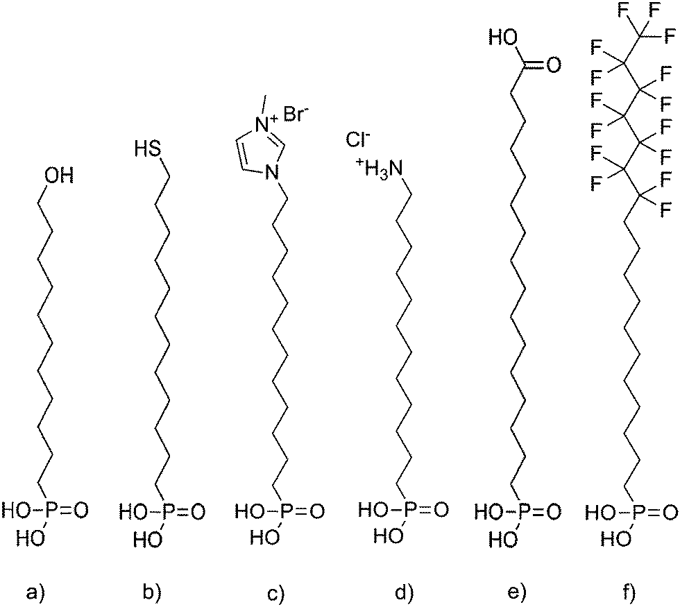 | ||
| Fig. 1 Molecular structures of the SAM molecules. (a) HO-C11-PA. (b) HS-C12-PA. (c) MIM+-C12-PA. (d) NH3+-C12-PA. (e) HOOC-C15-PA. (f) F15C18-PA. | ||
Scanning electron microscopy (SEM) characterization was performed with a Zeiss EVO 40, with the acceleration voltage of 8 kV, and electron beam current of 300 pA. Surface coverage was extracted using JMicrovision software (Roduit, N. JMicroVision: Image analysis toolbox for measuring and quantifying components of high-definition images. Version 1.2.7).
XPS measurements were carried out on ALD coated Si-wafers, which were activated in O2 plasma and subsequently dip-coated in 2-propanol solutions of MIM+-C12-PA and NH3+-C12-PA for 24 h. One series was measured as prepared, and the other series was treated with the reduction agents hydriodic acid (HI) and trifluoroacetic acid (TFA) at 80 °C before measurement. The XPS analysis was carried out using a Physical Electronics 5600 XPS setup with a monochromatized Al Kα X-ray source.
The FET devices fabrication relies on a photolithography process, which is based on a silicon wafer with 100 nm thermal oxide. The aluminum gate electrodes are patterned with a standard lift-off procedure, and the thickness of the gate electrodes is 30 nm. Before the self-assembly of the surfactant molecules, oxygen plasma (3 min, pressure 0.2 mbar, power 200 W) was applied. Afterwards, the wafer was kept in the solution of HS-C12-PA (0.2 mmol L−1, ∼65 h, 2-proponal as solvent) for SAM formation. The gold source/drain electrodes are patterned via a wet-etching process (KI/I2 solution as etchant), and the thickness of the resulting electrodes is 30 nm. The SAM in the channel region is then removed by oxygen plasma (10 min, pressure 0.2 mbar, power 200 W), and replaced with a new SAM (shown in Fig. 1a–e). The GO deposition was the final step by dip-coating in solution (0.1 mg mL−1, 7 °C, 24 hours), followed by a reduction process in a petridish on 80 °C hotplate. The reduction agents are vapor of HI and TFA, and the reduction time is 5 minutes. After the chemical reduction, the devices are ready to be measured.
Results and discussion
By using in-plane patterns of SAMs on flat substrates, silicon wafers covered with ALD aluminum oxide, it is possible to attribute the results of the deposition process only to the actual chemical nature of the surface, rather than the contrast in surface roughness, because the SAM molecules exhibit comparable chain lengths of about 2 nm. Monolayer patterns of PA SAMs were fabricated by photolithographic methods. The molecules are similar with respect to PA anchor groups and length of the alkyl chain (C11–C15), but differ in their head group termination. We used 11-hydroxyundecylphosphonic acid (HO-C11-PA), 12-mercaptododecylphosphonic acid (HS-C12-PA), 3-methyl-1-(12-phosphonododecyl)imidazolium bromide (MIM+-C12-PA), 12-phosphonododecan-1-ammonium chloride (NH3+-C12-PA) and 16-phosphonohexadecanoic acid (HOOC-C15-PA) for monolayer formation. The molecules of various chemical structures based on PA are proven to form densely packed SAMs and the utility of PA SAMs has been established as state-of-the-art.17,21 The contrast is built between the aforementioned molecules and 12,12,13,13,14,14,15,15,16,16,17,17,18,18,18-pentadecafluorooctadecyl-phosphonic acid (F15C18-PA), which is also formed by self-assembly on the remaining uncovered areas. All the molecules are displayed in Fig. 1. The GO was synthesized by a previously published procedure, which yields GO flakes with very low defect densities and almost intact carbon lattice.22,23 Since permanent defects within the σ-framework of carbon atoms of GO generally exclude full restoration of the carbon lattice, the quality of the used GO is of particular importance for device applications.24–26 Typical Raman spectra are depicted in Fig. S5† and the average quality of flakes of GO obtained after reduction was recently analyzed in depth, using statistical Raman microscopy.27The selectivity of the GO self-assembly was visualized by SEM. The SEM images taken from in-plane patterned samples (Fig. 2) show that the GO flakes do not assemble in areas covered by F15C18-PA layers. In the areas created by SAM molecules from Fig. 1a–e, a coverage was obtained, but with differences in coverage density. Molecules (Fig. 1a, b and e), which consist of uncharged head groups and provide only hydrogen bonding and dipole–dipole interaction forces, attract very few single flakes (Fig. 2b, c and f). SAMs with charged methylimidazolium and ammonium head groups (Fig. 1c and d) lead to much higher GO coverage density (Fig. 2d and e), as summarized in Table 1. The pronounced differences in surface coverage indicate that stronger Coulomb interaction (over 100 kJ mol−1 and even more in some ionic species)26 is favorable compared to weaker hydrogen bonding (∼25 kJ mol−1)28,29 or dipole interaction (∼1 kJ mol−1 at 1 Debye and 0.5 nm distance)28 to create densely packed GO layers. We note, that the self-assembly process leads to monolayer coverage of GO on the SAMs, because the repulsive forces resulting from GO functionalization do not only provide solubility but also prevent GO from stacking to multilayers.23
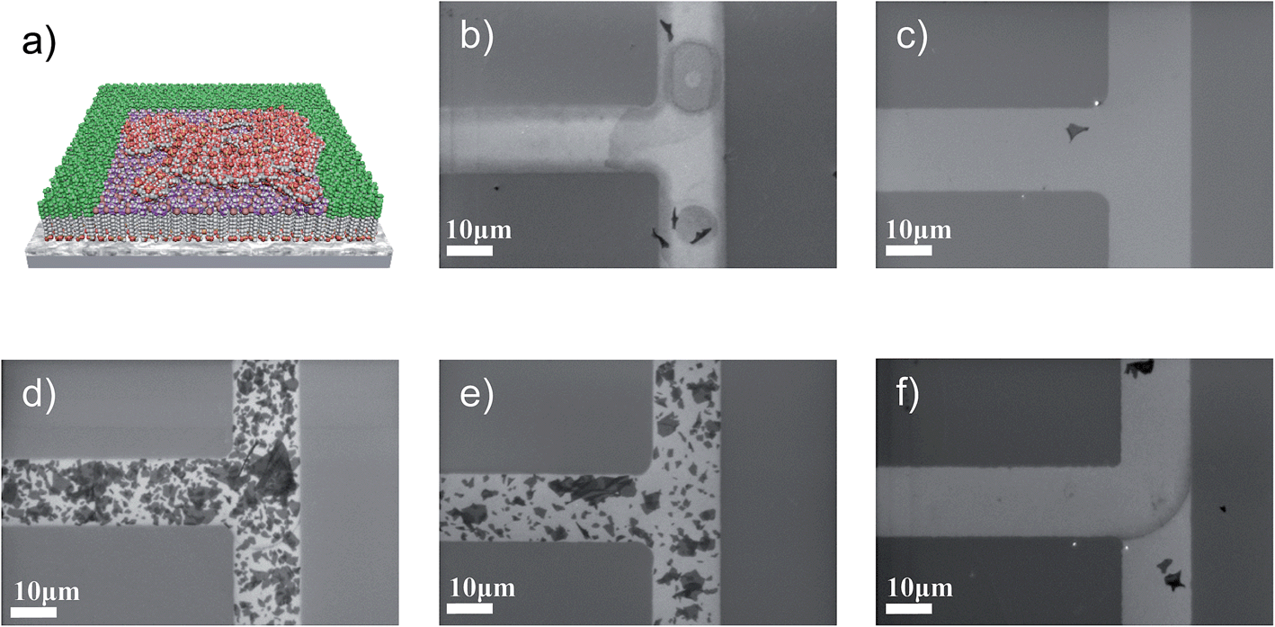 | ||
| Fig. 2 The self-assembly of GO on in-plane patterned SAM substrate. (a) Schematic cross section showing the assembly results. The active SAM in the middle is surrounded by F15C18-PA (in green). SEM images showing the GO flakes deposited on active in-plane patterned SAM, including (b) HO-C11-PA, (c) HS-C12-PA, (d) MIM+-C12-PA, (e) NH3+-C12-PA, and (f) HOOC-C15-PA. The scale bars are 10 μm. | ||
| Dielectric | Coverage [%] on flat surface | Coverage [%] on Al electrodes | Capacitance [μF cm−2] | Hole mobility [cm2 V−1 s−1] | Electron mobility [cm2 V−1 s−1] | Dipole moment [D] | Dirac voltage [V] |
|---|---|---|---|---|---|---|---|
| HS-C12-PA | <1 | 34 | 0.94 | 0.25 | 0.19 | −0.62 | 2.27 ± 0.18 |
| HO-C11-PA | 2 | 49 | 1.05 | 0.07 | 0.05 | 1.46 | 0.60 ± 0.39 |
| NH3+-C12-PA | 37 | 81 | 0.94 | 1.63 | 3.29 | 1.68 | 1.54 ± 0.10 |
| MIM+-C12-PA | 63 | 84 | 1.07 | 0.71 | 0.76 | 0.11 | 1.85 ± 0.35 |
| HOOC-C15-PA | 2 | 60 | 1.00 | 0.70 | 0.42 | 0.28 | 0.87 ± 0.25 |
The synthesis of GO leads to negative charges on the surface. It has been shown that GO prepared by a modified Hummer's method contains approximately one organosulfate group per 20 carbon atoms. Together with epoxy and hydroxyl groups these functionalities lead to a negative surface potential in GO of about −50 mV at pH 7.30,31 We kept the pH-value constant in order to obtain comparable results to the molecules with charged head groups. The self-assembly of the flakes can be clearly attributed to the Coulomb interaction between positively charged methylimidazolium or ammonium groups, and the negatively charged GO, especially organosulfate groups.30 It has been shown that organosulfate groups can be cleaved at certain reaction conditions or substituted by nucleophiles.32,33 Therefore, self-assembly was performed at 7 °C, despite the fact that the carbon framework of the used GO is stable up to 100 °C.34 Because the oxygen-moieties in GO, such as carboxyls, hydroxyls or epoxy groups, may also be able to engage in dipole–dipole interactions or hydrogen bonding with SAM head groups, this type of attraction also has to be considered and may contribute. However, the SEM images of self-assembly results from HS-C12-PA, HO-C11-PA and HOOC-C15-PA show very low GO coverage of less than 3%. On that account, we conclude that the attractive force between dipoles or hydrogen bonding is too weak for effective self-assembly of GO flakes from solution. The resulting coverage of the GO flakes suggests that the polarity of the SAM molecule and the resulting intermolecular forces only play a secondary role in the deposition process due to the lower interaction strength.
To apply the selective deposition to device architecture, the self-assembly process has to be verified on integrated device features such as metal gate electrodes, where the surface roughness plays a significant role. Patterned samples with the dedicated SAM on 30 nm aluminum structures surrounded by the F15C18-PA contrast layer were fabricated as described above, and the resulting SEM images are presented in Fig. 3. Compared to the in-plane pattern with a roughness of RRMS = 0.5 nm (Fig. 2), these substrates exhibit an increased roughness RRMS of 1.3 nm, which leads to a decreased height uniformity of the SAM head groups but still densely packed SAMs.17,23 The increased surface roughness simply provides additional nucleation sites for diffusion controlled assembly of the GO flakes, which leads to a general significant increase in GO coverage on the SAM-functionalized aluminum electrodes (Fig. 3b–f). The corresponding quantitative coverage figures are summarized in Table 1. On rough gate surfaces, GO self-assembly was obtained for all SAMs, but the differences in coverage density follow the same trend related to the molecular structure and interaction strength of the head groups. The highest coverage of 84% and 81% is achieved on MIM+-C12-PA and NH3+-C12-PA SAMs. The uncharged SAMs with hydrogen bonding head groups (HOOC-C15-PA, HO-C11-PA and HS-C12-PA) exhibit a decreased coverage of 60%, 49%, and 34%, respectively. This means that the MIM+-C12-PA attracts more than twice as much GO flakes than the polar HS-C12-PA. These results clearly show that surface roughness contributes significantly in self-assembly and might be considered in discussion on chemical interactions in general.
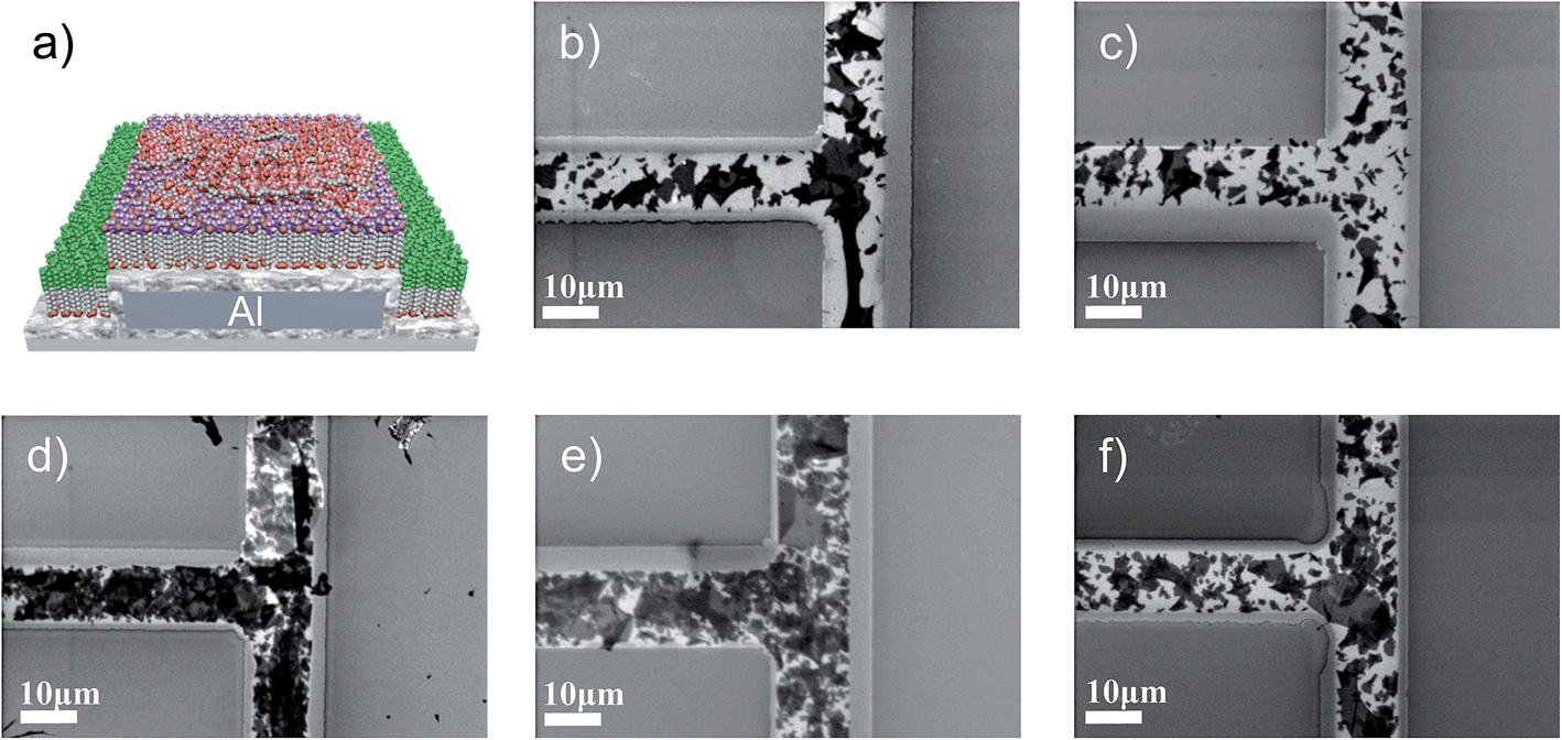 | ||
| Fig. 3 The self-assembly of GO on patterned Al gate electrodes substrate. (a) Schematic cross section showing the assembly results. The Al gate is functionalized with active SAMs, and surrounded by F15C18-PA. SEM images showing the GO flakes deposited on active SAM, including (b) HO-C11-PA, (c) HS-C12-PA, (d) MIM+-C12-PA, (e) NH3+-C12-PA, and (f) HOOC-C15-PA. The scale bars are 10 μm. | ||
Although the functional groups in GO are beneficial for solubility and the self-assembly process, their introduction completely destroys the electrical properties of graphene. By reducing the GO, the oxygen and sulfur species are removed and the sp3 hybridized carbon atoms are reconverted to their initial sp2 based hexagonal lattice. Thus, rGO becomes conductive again. Statistical Raman-measurements have shown that the reduction of the GO used in this work yields graphene with a residual defect density below 0.3% in average, corresponding to an average defect spacing of more than 3 nm, which is suitable to make GO applicable for electronic applications.22,27,35,36
To proof that our SAMs sustain the harsh reduction process without alterations to their chemical nature, XPS measurements were performed on substrates functionalized with MIM+-C12-PA and NH3+-C12-PA SAMs before and after the treatment with reduction agents. We have chosen these examples because of their promising surface coverage with GO. The XPS spectra in Fig. 4 show the C 1s and N 1s signals of the functional groups (the other relevant core levels are shown in Fig. S6 and S7†). In case of the MIM+-C12-PA, the dominant features of the C 1s region are the signal of the alkyl chain carbons at 284.0 eV, and the signal of the carbon atoms bound to the heteroatoms in the imidazolium ring, which is shifted to 285.5 eV. In the N 1s region, the peak of the imidazolium nitrogen atoms is detected at 401.4 eV. After reduction, the positions of the relevant peaks do not change. For the NH3+-C12-PA functionalized samples, the main C 1s peak of the alkyl chain carbon atoms is detected at 284.8 eV, while the small shoulder at 286.0 eV is attributed to the nitrogen-bound carbon atoms. NH3+-moieties are revealed by the N 1s peak at 401.3 eV. This binding energy confirms the presence of the positively charged ammonium groups, since uncharged free amines would appear at ∼399.5 eV.37 After reduction, the peaks observed in the initial NH3+-C12-PA spectra remain at the same positions. In both investigated SAMs, the relative atomic concentrations of the SAM-related signals decrease after reductive treatment and at the same time, the oxygen and aluminum signals originating in the underlying aluminum oxide layer increase. This effect is less pronounced for the NH3+-C12-PA functionalized sample. The unchanged energy positions show that the SAM head groups are not subject to any chemical alterations due to the treatment with HI and TFA. However, the decrease of the N 1s peaks in Fig. 4 and also of the P 2p peaks at 131.9 eV (see ESI†) suggest a lower monolayer density after reduction; this is also reflected in an increase of the substrate in Al 2p and O 1s signals at 73.2 and 532.5 eV (see ESI†) due to the less pronounced damping effect by the monolayer with smaller density. The comparable decrease of the N 1s and P 2p intensities to 46% and 49% (±7%), respectively, for MIM+-C12-PA, and to 73% and 72% (±5%), respectively, for NH3+-C12-PA, is a further indication that both SAMs are intact after the reduction step. The lower decrease of the C 1s signals in Fig. 4 is most likely due to carbonaceous contaminations, which are more pronounced for the remaining more dilute SAM layers. The XPS measurements show that although the monolayer density is slightly decreased, the SAMs are still chemically intact after reduction, and can be applied as dielectric layers in FET devices. Furthermore, to evaluate the impact of the reduction step on the SAMs, one has to consider the fact that the major part of the active monolayer area is covered and shielded by GO flakes in the device fabrication process.
 | ||
| Fig. 4 C 1s and N 1s XPS detail spectra of (a) MIM+-C12-PA, and (b) NH3+-C12-PA, before and after the treatment with reduction agents. | ||
By applying the self-assembly of GO on aluminum electrodes, functional FETs could be realized for all SAMs, showing that even lower surface coverage (Table 1) leads to electrically connected flakes in the channel region. We fabricated FETs with hybrid aluminum oxide/SAM gate dielectric and bottom gold contacts. The GO was self-assembled in the active channel region and subsequently reduced by HI and TFA in the gas phase. The architecture of the device with a Corbino structure is shown in Fig. S8a.† The typical device channel length is 5 μm and channel width is 1000 μm. Representative transfer curves are shown in Fig. 5 for different SAM head groups. The devices exhibit hole transport with low current ratios between 1.5 and 2.1, which is the typical transport behavior of rGO devices. The device mobilities, which are calculated from the linear region transport model of a thin-film transistor,23 are summarized in Table 1 as well. The calculation is based on the capacitance of the hybrid dielectric aluminum oxide and SAM, which is also shown in Table 1. The device mobility also correlates with the surface coverage. The SAMs, on which GO flakes have higher surface coverage, especially the ones providing Coulomb attractions (NH3+-C12-PA, MIM+-C12-PA), lead to higher mobilities for both holes and electrons. We also observed a shift in the Dirac point due to the influence of the SAM head groups on the electronic structure of the rGO in the channel. The calculation method of the dipole moments for different SAMs can be found in ESI.† The data shown in Fig. 5a suggests that SAM molecules with higher z-component of the SAM dipole moment, taking the sign of dipole moment into account, tend to shift the Dirac point to smaller positive values. This can be attributed to an electrostatic doping from the dipole moment of the underneath SAM molecules.20,38 Due to the larger surface coverage of rGO on the charged SAMs such as MIM+-C12-PA and NH3+-C12-PA, a much higher drain current level (higher than 1 mA) was obtained, compared to devices with non-charged SAMs. All the output curves for different SAMs are shown in Fig. S8.† If the devices could be scaled to smaller dimensions, the device resistance would be largely reduced and the performance would be enhanced, since all the connections between source and drain would be just single flakes in parallel, and hence the flake–flake hopping resistance would no longer exist.
 | ||
| Fig. 5 The electric properties of the rGO FET based on different SAM molecules. (a) The Dirac voltage versus dipole moment of the SAM molecules. The plot is extracted from the transfer curves of the rGO FET built on the SAM molecules of (b) HO-C11-PA, (c) HS-C12-PA, (d) MIM+-C12-PA, (e) NH3+-C12-PA, and (f) HOOC-C15-PA. The Dirac points are marked with the red arrows. The drain voltage is set to 1 V, and all the measurement is carried out in ambient. | ||
Conclusions
In conclusion, we demonstrate a method for the site-selective deposition of GO on in-plane SAM patterns and SAMs on rough surfaces as FET gate pattern. The strongest driving force of the self-assembly is attributed to Coulomb interactions between negatively charged functional groups in the GO framework and positively charged SAM head groups. Different SAM head groups can be used to adjust the Coulomb driving force and the resulting GO surface coverage. XPS investigations showed that the reduction treatment used for the conversion of GO to rGO does not change the chemical nature of the SAM head groups, but slightly compromises the density of the monolayers. As demonstration for connected rGO flakes we fabricated FET devices based on different SAM head groups, resulting in a shift in the Dirac voltage due to the different dipole moment of the SAM molecules. The current level of the transistors also depends on the coverage density of the self-assembled flakes, which relate to the driving force of the self-assembly process.Acknowledgements
We gratefully acknowledge the German Research Council (DFG) with the Collaborative Research Center (SFB-953) and the Erlangen Graduate School of Molecular Science (GSMS) for financial support.References
- K. S. Novoselov, Science, 2004, 306, 666 CrossRef CAS PubMed.
- M. F. Craciun, I. Khrapach, M. D. Barnes and S. Russo, J. Phys.: Condens. Matter, 2013, 25, 423201 CrossRef CAS PubMed.
- Z. Wang, Z. Zhang and L. Peng, Chin. Sci. Bull., 2012, 57, 2956 CrossRef CAS.
- T. Mueller, F. Xia and P. Avouris, Nat. Photonics, 2010, 4, 297 CrossRef CAS.
- N. O. Weiss, H. Zhou, L. Liao, Y. Liu, S. Jiang, Y. Huang and X. Duan, Adv. Mater., 2012, 24, 5782 CrossRef CAS PubMed.
- M. Freitag, T. Low, F. Xia and P. Avouris, Nat. Photonics, 2013, 7, 53 CrossRef CAS.
- F. Schwierz, Nat. Nanotechnol., 2010, 5, 487 CrossRef CAS PubMed.
- E. Guerriero, L. Polloni, M. Bianchi, A. Behnam, E. Carrion, L. G. Rizzi, E. Pop and R. Sordan, ACS Nano, 2013, 7, 5588 CrossRef CAS PubMed.
- J. Lee, T.-J. Ha, H. Li, K. N. Parrish, M. Holt, A. Dodabalapur, R. S. Ruoff and D. Akinwande, ACS Nano, 2013, 7, 7744 CrossRef CAS PubMed.
- C. Mattevi, H. Kim and M. Chhowalla, J. Mater. Chem., 2011, 21, 3324 RSC.
- V. Georgakilas, M. Otyepka, A. B. Bourlinos, V. Chandra, N. Kim, K. C. Kemp, P. Hobza, R. Zboril and K. S. Kim, Chem. Rev., 2012, 112, 6156 CrossRef CAS PubMed.
- S. Park and R. S. Ruoff, Nat. Nanotechnol., 2009, 4, 217 CrossRef CAS PubMed.
- C. Wu, Q. Cheng, S. Sun and B. Han, Carbon, 2012, 50, 1083 CrossRef CAS PubMed.
- H. Y. Cho, C. J. Han and I. In, Chem. Lett., 2012, 41, 290 CrossRef CAS.
- D. Chen, H. Feng and J. Li, Chem. Rev., 2012, 112, 6027 CrossRef CAS PubMed.
- Z. Wei, D. E. Barlow and P. E. Sheehan, Nano Lett., 2008, 8, 3141 CrossRef CAS PubMed.
- M. Halik and A. Hirsch, Adv. Mater., 2011, 23, 2689 CrossRef CAS PubMed.
- H. Chen and X. Guo, Small, 2013, 9, 1144 Search PubMed.
- C. Mattevi, F. Colléaux, H. Kim, Y.-H. Lin, K. T. Park, M. Chhowalla and T. D. Anthopoulos, Nanotechnology, 2012, 23, 344017 CrossRef PubMed.
- N. Cernetic, S. Wu, J. A. Davies, B. W. Krueger, D. O. Hutchins, X. Xu, H. Ma and A. K.-Y. Jen, Adv. Funct. Mater., 2014, 22, 3464 CrossRef PubMed.
- H. Ma, O. Acton, D. O. Hutchins, N. Cernetic and A. K.-Y. Jen, Phys. Chem. Chem. Phys., 2012, 14, 14110 RSC.
- S. Eigler, M. Enzelberger-Heim, S. Grimm, P. Hofmann, W. Kroener, A. Geworski, C. Dotzer, M. Röckert, J. Xiao, C. Papp, O. Lytken, H.-P. Steinrück, P. Müller and A. Hirsch, Adv. Mater., 2013, 25, 3583 CrossRef CAS PubMed.
- Z. Wang, S. Mohammadzadeh, T. Schmaltz, J. Kirschner, A. Khassanov, S. Eigler, U. Mundloch, C. Backes, H.-G. Steinrueck, A. Magerl, F. Hauke, A. Hirsch and M. Halik, ACS Nano, 2013, 7, 11427 CrossRef CAS PubMed.
- S. Pei and H.-M. Cheng, Carbon, 2012, 50, 3210 CrossRef CAS PubMed.
- S. Mao, H. Pu and J. Chen, RSC Adv., 2012, 2, 2643 RSC.
- C. K. Chua, A. Ambrosi and M. Pumera, J. Mater. Chem., 2012, 22, 11054 RSC.
- S. Eigler, F. Hof, M. Enzelberger-Heim, S. Grimm, P. Müller and A. Hirsch, J. Phys. Chem. C, 2014, 118, 7698 CAS.
- P. Atkins and J. de Paula, Physical Chemistry, Oxford University Press, 2006 Search PubMed.
- IUPAC, Compendium of Chemical Terminology, ed. A. D. McNaught and A. Wilkinson, Blackwell Scientific Publications, Oxford, 2nd edn, the “Gold Book”, 1997, XML on-line corrected version: http://goldbook.iupac.org (2006-) created by M. Nic, J. Jirat and B. Kosata, updates compiled by A. Jenkins, [Online] 2012 Search PubMed.
- S. Eigler, C. Dotzer, F. Hof, W. Bauer and A. Hirsch, Chem.–Eur. J., 2013, 19, 9490 CrossRef CAS PubMed.
- D. Li, M. B. Müller, S. Gilje, R. B. Kaner and G. G. Wallace, Nat. Nanotechnol., 2008, 3, 101 CrossRef CAS PubMed.
- S. Eigler, S. Grimm, F. Hof and A. Hirsch, J. Mater. Chem. A, 2013, 1, 11559 CAS.
- S. Eigler, Y. Hu, Y. Ishii and A. Hirsch, Nanoscale, 2013, 5, 12136 RSC.
- S. Eigler, S. Grimm and A. Hirsch, Chem.–Eur. J., 2014, 20, 984 CrossRef CAS PubMed.
- S. Eigler, S. Grimm, M. Enzelberger-Heim, P. Müller and A. Hirsch, Chem. Commun., 2013, 49, 7391 CAS.
- J. M. Englert, P. Vecera, K. C. Knirsch, R. A. Schäfer, F. Hauke and A. Hirsch, ACS Nano, 2013, 7, 5472 CrossRef CAS PubMed.
- M.-L. Abel, S. Suzer, J. F. Watts, P. M. Dietrich, N. Graf, T. Gross, A. Lippitz, S. Krakert, B. Schüpbach, A. Terfort and W. E. S. Unger, Surf. Interface Anal., 2010, 42, 1184 CrossRef PubMed.
- M. Salinas, C. M. Jäger, A. Y. Amin, P. O. Dral, T. Meyer-Friedrichsen, A. Hirsch, T. Clark and M. Halik, J. Am. Chem. Soc., 2012, 134, 12648 CrossRef CAS PubMed.
Footnotes |
| † Electronic supplementary information (ESI) available. See DOI: 10.1039/c4nr02527j |
| ‡ Both authors contributed equally to this work. |
| This journal is © The Royal Society of Chemistry 2014 |