 Open Access Article
 This Open Access Article is licensed under a
 Creative Commons Attribution 3.0 Unported Licence
In situ TEM analysis of resistive switching in manganite based thin-film heterostructures†
Jonas
Norpoth
,
Stephanie
Mildner
,
Malte
Scherff
,
Jörg
Hoffmann
and
Christian
Jooss
*
Institut für Materialphysik, Universität Göttingen, Friedrich–Hund–Platz 1, 37077 Göttingen, Germany. E-mail: jooss@material.physik.uni-goettingen.de
First published on 26th June 2014
Abstract
The mechanism of the electric-pulse induced resistance change effect in Au/Pr0.65Ca0.35MnO3/SrTi0.99Nb0.01O3 thin-film samples is studied by means of in situ electrical stimulation inside a transmission electron microscope. A detailed equivalent-circuit model analysis of the measured current–voltage characteristics provides crucial information for the proper interpretation of the microscopy results. The electrical transport data of the electron-transparent samples used for the in situ investigations is verified by comparison to measurements of unpatterned thin-film samples. We find comprehensive evidence for electrochemical oxygen vacancy migration affecting the potential barrier of the pn junction between Pr0.65Ca0.35MnO3 and SrTi0.99Nb0.01O3 as well as the resistance of the manganite bulk. The high-resistance state formation in the Pr0.65Ca0.35MnO3 bulk is frequently accompanied by structural transformations, namely detwinning and superstructure formation, most likely as the result of the joint impact of dynamic charge inhomogenities by oxygen vacancy migration and injection of high carrier densities at the electrodes.
1 Introduction
Since the discovery of the electric-pulse induced resistance change effect (EPIR) in Pr0.7Ca0.3MnO3,1 nonvolatile resistive switching has been revealed in a variety of complex transition-metal oxide based devices.2,3 Due to the demonstrated fast switching between well defined high- and low-resistance states (HRS, LRS) in capacitor-like devices, this class of materials is among the candidates for the resistance random access memory (ReRAM) concept being explored as an alternative to the contemporary flash memory.4–7In metal/Pr0.7Ca0.3MnO3/metal thin-film devices, the largest switching ratios (up to RHRS/RLRS ≈ 1000) are found for electrodes made of non-noble metals, e.g. Ta,8 Al,9 and Ti.10 The switching logic in these devices is of the bipolar type, i.e. a reversal of the applied pulse voltage is required to switch between HRS and LRS. This behaviour has been ascribed to electrochemical formation/growth and dissolution of an interfacial metal-oxide layer, where the manganite merely acts as an oxygen reservoir.11–13 Devices with noble-metal electrodes exhibit significantly lower, if any, switching ratios,9,12,14,15 whose physical origin is a matter of some controversy. There is general consensus on the important role played by electrically induced electronic inhomogenities, but their primal source and manifestations are discussed in different frameworks like oxygen vacancy electromigration,16,17 Mott transition,14,18 charge carrier injection and trapping,3,19 or current-induced structural phase transitions.20 While most of these mechanisms are mainly associated with the interfacial region of the devices, also resistive switching of the Pr0.7Ca0.3MnO3 film bulk was directly observed by means of Kelvin probe microscopy.21
In this contribution, we address the question of the switching mechanism in Au/Pr0.65Ca0.35MnO3 (PCMO) based thin-film samples by means of in situ transmission electron microscopy (TEM). This technique, where a piezo-driven, metallic nano-tip is used to contact and electrically stimulate an electron-transparent sample inside the microscope, has already been applied to monitor resistive-switching related oxygen vacancy migration in PCMO and other transition-metal oxides,17,22,23 as well as corresponding structural phase transitions.20,24–26 The high spatial-resolution capabilities of TEM in both imaging and electron-spectroscopy modes allow for indivdual addressing of PCMO bulk, electrodes and interfacial regions respectively in order to detect potential electrically induced changes.
Our PCMO films are epitaxially grown on electron-doped SrTi0.99Nb0.01O3 (STNO) substrates forming a pn heterojunction with rectifying transport properties.27,28 As will be discussed later by means of an equivalent-circuit model, the contribution of the bottom interface forming the pn junction as well as that of the actual PCMO film and its interface to the Au top electrode can be assigned to different regimes of the current–voltage characteristics. Complementary to the TEM investigations, this feature of our samples provides additional information about the resistive switching loci directly from the electrical transport data.
A proper comparison of the in situ transport characteristics acquired from electron-transparent samples (referred to as “TEM-samples” in the following) with data from unpatterned thin-film samples (“pad-samples”) is conducted in order to validate the information revealed by the TEM investigations. In this context, the sensitivity of the pn junction current–voltage characteristics on defects and surface states is a useful probe for peculiarities of the TEM-samples, possibly introduced by intrinsic surface effects or surface damage from the sample preparation process, see e.g.ref. 29.
The manuscript is organized as follows: after a description of the experimental details, an equivalent-circuit model is proposed and initially applied to the current–voltage characteristics in a voltage regime below the onset of resistive switching. Afterwards, the EPIR is demonstrated in both types of samples and comparatively analysed. Finally, we present and discuss the results of the in situ TEM investigations.
2 Experimental procedure
Epitaxial pn heterojunctions were fabricated by reactive ion-beam sputtering from a stoichiometric PCMO target at a deposition temperature of 750 °C and an oxygen partial pressure of 10−4 mbar. Thin films with thickness d = 200–370 nm were deposited at a rate of 5 nm min−1 on polished STNO(100) substrates (5 × 10 mm2; CrysTec). Pre- (post-) deposition heating (cooling) took place at the aforementioned oxygen partial pressure and at a rate of 25 °C min−1. The electrodes are Ti contacts with a thin Au protection coating on STNO and Au contacts on PCMO. All metal electrodes were sputter deposited into shadow masks (1 × 3 mm2 notches) at 110 °C.In the case of the pad-samples, a permanent photo-resist layer (Allresist AR-U 4040) with lithographically generated circular holes (diameters 3–7 μm) was placed between PCMO and the shadow mask in order to confine the top electrode contact area to the hole diameter (see Fig. 1(a)).
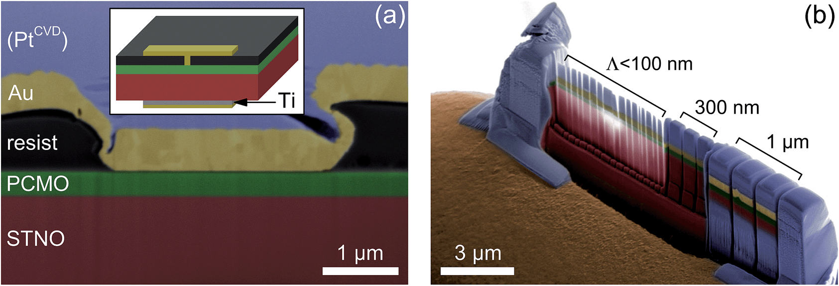 | ||
| Fig. 1 RGB-colored SEM micrographs of the two types of samples. (a) Cross section through pad-sample. The PtCVD capping is not present in the active state of the sample. Inset: schematic overview. (b) TEM-sample on Cu support with teeth of different dimensions. | ||
TEM-samples were prepared by focused ion beam (FIB) technique with a FEI Nova Nano Lab 600. Lamellae of 10–20 μm width were milled as cross-sections of Au/PCMO/STNO samples and glued on Cu supports by means of chemical vapour deposited Pt (PtCVD). The lamellae were then thinned with 30 keV Ga+ ions under grazing incidence of α = 1–2° and afterwards cleaned with 5 keV Ga+ and α = 5°. The final thickness of the various samples covers a range Λ = 50–1000 nm (in electron propagation direction in the TEM). In order to provide well defined cross sections for the electrical characterisation, the lamellae were finally cut into separate, 0.5–2 μm wide ”teeth” by FIB milling from the top (α = 0°). The electrical back contact is provided by the remainder STNO conductively glued to the Cu support (see Fig. 1(b)).
Electrical characterisation was performed with voltage pulses of 2 ms duration and 45 ms period from a programmable Keithley 2430 sourcemeter in two-point configuration. A positive (negative) sign of the applied voltage corresponds to the forward (reverse) direction of the pn junction. One or multiple intermediate pulses at low forward bias were applied between the (incremental) bias pulses in a current–voltage cycle (cf. sketch in Fig. 1(a) of ref. 15). This scheme was implemented in order to monitor potential resistance relaxations after high-power pulses, e.g. as a probe for Joule heat dissipation. In the EPIR regime at high voltages, the intermediate pulses are also useful to determine quasi simultaneously the impact of the resistive switching on the low-bias characteristics, which is rewarding, since the respective regimes of the current–voltage curves are associated with different entities of the equivalent-circuit model (see below). For the TEM investigations, the electrical connection to the TEM-samples was provided by a dedicated in situ TEM holder (Nanofactory) with a piezo-controlled Pt/Ir nano-tip and feed line to the sample support.
The in situ TEM investigations were performed in a Philips CM30 microscope and in a FEI Titan equipped with a GIF Quantum spectrometer, including microscopy techniques like bright field (BF), dark field (DF), annular dark field (ADF) and energy filtered (EFTEM) imaging, selected area diffraction (SAD) and electron energy-loss spectroscopy (EELS). Details of the data analysis for EFTEM and EELS data can be found in the ESI.†
3 Electrical transport properties
3.1 Rectifying characteristics and equivalent-circuit analysis
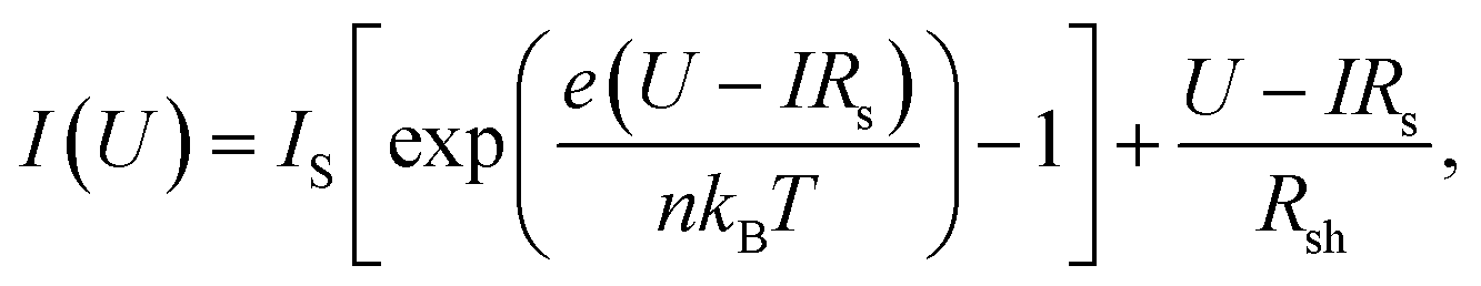
The rectifying current–voltage characteristics of the samples were analysed in terms of numerical simulations of an equivalent-circuit model. This circuit consists of a non-ideal Schottky diode with a reverse bias saturation current IS and an ideality factor n, a series resistance Rs and a parallel shunt resistance Rsh (see inset of Fig. 2(a)). The corresponding current–voltage relation is given bywherein e and kBT are the elemental charge and the thermal energy, respectively. Fitting as much as four parameters to experimental current–voltage curves in a consistent manner is only possible because each parameter affects the data in a characteristic way and primarily in a selective voltage interval: the reverse bias region in our samples is entirely dominated by Rsh, whereas in forward bias IS sets the turn-on voltage of the diode, n determines the maximum slope and Rs limits the current at high voltages (see ESI-Fig. 2†).
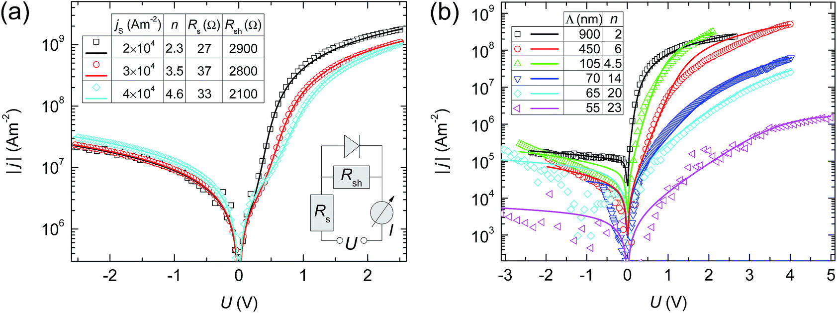 | ||
| Fig. 2 Initial current–voltage characteristics: experimental (symbols) and simulated (lines) data. (a) Characteristic pad-samples. Top inset: fit parameters. Bottom inset: sketch of the equivalent circuit. (b) Range of TEM-samples. Inset: lamella thickness vs. fitted ideality factor. | ||
In contrast to the geometrically confined TEM-samples, the effective current-carrying cross section in pad-samples is not rigidly defined (see Fig. 1(a)). In particular, there is an asymmetry with respect to the bias polarity, since the primary voltage drop occurs over the diode and the shunt resistance under reverse bias, but over the series resistance in forward direction (see later Fig. 3(d)). Consequently, the (high-bias) forward current scales properly with the top electrode contact area, while it is nearly invariant in reverse direction. Bearing this peculiarity in mind, we normalize the current through the pad-samples with the respective top electrode contact areas throughout the following analysis.
 | ||
| Fig. 3 Electric-pulse induced resistive switching. (a) Pad-sample. Insets: resistance in single intermediate pulses of 0.05 V forward bias between the incremental pulses in the branches 2 and 3 of the main panel. (b) Thick TEM-sample (Λ = 900 nm). Inset: time evolution of the resistance in multiple intermediate pulses of 0.3 V forward bias after each pulse of branch 4. (c) Thin TEM-sample (Λ = 55 nm). Inset: fit parameters. Arrows indicate the direction of the voltage loops in all viewgraphs. (d) Fractional voltage drop across pn junction (full lines) and series resistance (dashed) for our equivalent-circuit model with parameter sets corresponding to the respective initial current–voltage curves in the subfigures (a)–(c) (thick black, medium red, thin blue). | ||
Typical diode fit parameters in pad-samples are saturation current densities js = 104 to 105 Am−2 and ideality factors covering a range of n = 2–5. A closer examination of these numbers will be given below in the context of the TEM-samples.
The series resistance in the pad-samples is dominated by the resistance of the PCMO film and its contact resistance with the Au electrode. The resistivity of our PCMO films amounts to ρPCMO = 1.5 × 10⁻³ Ωm (cf. also ref. 30). We determined various metal/PCMO contact resistivities by measurements of metal/PCMO/metal stack combinations, where we extrapolated from PCMO film thickness series to zero thickness. For Au/PCMO we find a contact resistivity δC = 7.5 × 10⁻¹⁰ Ωm2. We measured the resistivity of STNO to be ρSTNO = 3 × 10⁻⁴ Ωm, but given its large cross section in the samples its contribution to the overall resistance is negligible. We checked both Ti and PtCVD back electrodes to form ohmic contacts with the STNO and confirmed the ohmic resistivity of PtCVD with ρpt:CVD = 1 × 10⁻⁵ Ωm. All numbers are given for room temperature. The major simplification in the model Rs lies in its ohmic character: due to the polaronic nature of its charge carriers, the resistances of both the PCMO and its contact to the Au are known to be current dependent.31 However, introducing an extra parameter for the nonlinearity of Rs leads to strong redundance in the data fitting and was thus not eventually implemented in the simulations. Below a current density of 109 Am−2 the committed error due to the ohmic approximation should be tolerable,31 and we find indeed a satisfying fit accuracy with an ohmic Rs model up to the onset of the EPIR regime: Fig. 2(a) shows typical initial current–voltage curves of pad-samples (all three with d = 370 nm and top electrode contact area A = π(3.5 μm)2) and the corresponding model data. Given the above numbers, Rs = ρPCMO·d/A + δc/A = 34 Ω is expected, which is in good agreement with the fitted values. The shunt resistance in the pad-samples dominates the reverse bias regime. It is voltage-independent within the measured range and best modeled by an ohmic resistance Rsh ≈ 2500 Ω. As stated above, we argue that substantial widening of the effective sample cross section under reverse bias yields such poor rectifying properties. As will be shown in the following paragraph, Rsh is subject to remanent, bipolar resistance changes in the EPIR regime and we thus conclude that its primary origin is of intrinsic nature, i.e. a property of the PCMO/STNO junction and not a process-induced shortage like leakage across the sample edges. Microstructural entities possibly acting as shunts are misfit dislocations and boundaries between epitaxial twins in the PCMO film as well as small interfacial Mn2O3 nanoparticles that we find at an area density of ∼1 μm−2 in TEM/SEM investigations, see ESI-Fig. 3.† These nanoparticles are insulating themselves but may provide conducting channels in their close circumference, e.g. by inversion layer formation.32 However, the shunt resistances in TEM-samples exhibit no appreciable differences whether nanoparticles are contained or not. This points to a primary leakage mechanism based on band-to-band-tunneling across the pn junction.33–35 Given the high doping levels in both materials, the depletion layer only has a width on the order of 1 (10) nm on the PCMO (STNO) side of the junction.28 The corresponding high electric fields across the reverse-biased junction (∼108 V m−1 at 1 V applied) give rise to significant current flow by tunneling of electrons from the valence band of the p region into the conduction band of the n region.
Fig. 2(b) shows initial current–voltage characteristics of TEM-samples. There are two striking observations: a strong dependency on the lamella thickness Λ and a reduced fitting accuracy with the proposed equivalent-circuit model. In the following we specify the differences between the two types of samples.
With 2 < n < 6 and js = 104−5 × 10⁵ Am−2 the fitted diode parameters of thick TEM-samples (Λ > 100 nm) closely resemble those of the pad-samples. However, further thinning strongly increases the ideality factor to n > 30. The ideality factor reflects carrier recombination processes associated with the pn junction: the ideal, defect-free diode with a current exclusively based on diffusion is characterized by n = 1. The introduction of (independent) traps inside the band gap of the junction gives primarily rise to Shockley–Read–Hall recombination and covers 1 < n ≤ 2.36,37 Higher n values were ascribed to recombination at coupled defects,38 tunneling-enhanced recombination at the interface or in the space-charge region,39,40 and to multi-step recombination-tunneling.41 Brötzmann et al. modeled giant apparent ideality factors by an interfacial disordered or amorphous layer with Frenkel–Poole conduction properties.42 We attribute the recombination enhancement in our TEM-samples in part to ion beam induced disorder and defect formation. Binary collision Monte Carlo simulations of the 30 keV FIB milling process show amorphisation of a 5 nm thick surface layer and an atomic recoil distribution with tails reaching as deep as 15 nm into the lamellae.43 Similar results are reported for FIB-processed TEM samples from LaAlO3/SrTiO3 multilayers,44 and even heavier damage formation for Si,45 and AlGaAs lamellae.46 Since SAD investigations never proved any evidence for amorphous material in our samples, we are confident that the final 5 keV cleaning procedure removes the most heavily damaged portion of the surface layer. Nonetheless, the long-reaching recoil tails possibly have an impact on the junction recombination rates. Another reason of the large n values in thin samples might arise from an increased relative contribution of intrinsic surface states. Dong et al. predicted surface reconstructions in low-bandwidth manganites like PCMO that exhibit ferromagnetic–metallic tendencies in contrast to the antiferromagnetic, charge-ordered bulk phase.47 Emergent ferromagnetism was indeed observed experimentally in nanoparticles of appropriate manganites.48–50 Such metallic surface states could provide additional recombination channels contributing to the modified junction characteristics of our TEM-samples.
The magnitude of the saturation current is only affected below Λ < 60 nm, where it eventually declines to the order of js ∼ 103 Am−2.
The series resistance in the measurements of TEM-samples is 2–5 fold higher than expected based on the values obtained in the pad-samples. We observed that the contact resistance between nano-tip and top electrode yields the dominant extra-contribution in our experiments, since repositioning, shifting or pushing the nano-tip in contact with the sample can significantly alter Rs. With regard to the EPIR properties, changes in the series resistance of the actual sample can thus only be studied if a low-resistive contact with the nano-tip has been carefully established.
The shunt resistance in TEM-samples exhibits voltage dependence as can be seen in the poor fit accuracy of the reverse branches in Fig. 2(b). A coarse estimate with an ohmic equivalent yields a sheet resistivity on the order of δsh ∼10−5 Ωm2, which increases up to ∼10−3 Ωm2 for Λ < 60 nm. The nonlinearity, which is most pronounced in the thinnest samples, is presumably also introduced by the surface states providing leakage paths that bypass the pristine band-to-band-tunneling and dominate the reverse current in TEM-samples.
In comparison, the rectifying current–voltage characteristics of pad-samples are basically reproduced in TEM-samples. Surface effects affect the diode parameters of the pn junction in thin lamellae and some experimental care is needed to provide a meaningful Rs, which is not dominated by the contact resistance with the nano-tip. The major limitation is the inaccessibility of the pristine PCMO/STNO shunt resistance, which is paralleled by the surface state contributions in TEM-samples.
3.2 Resistive switching
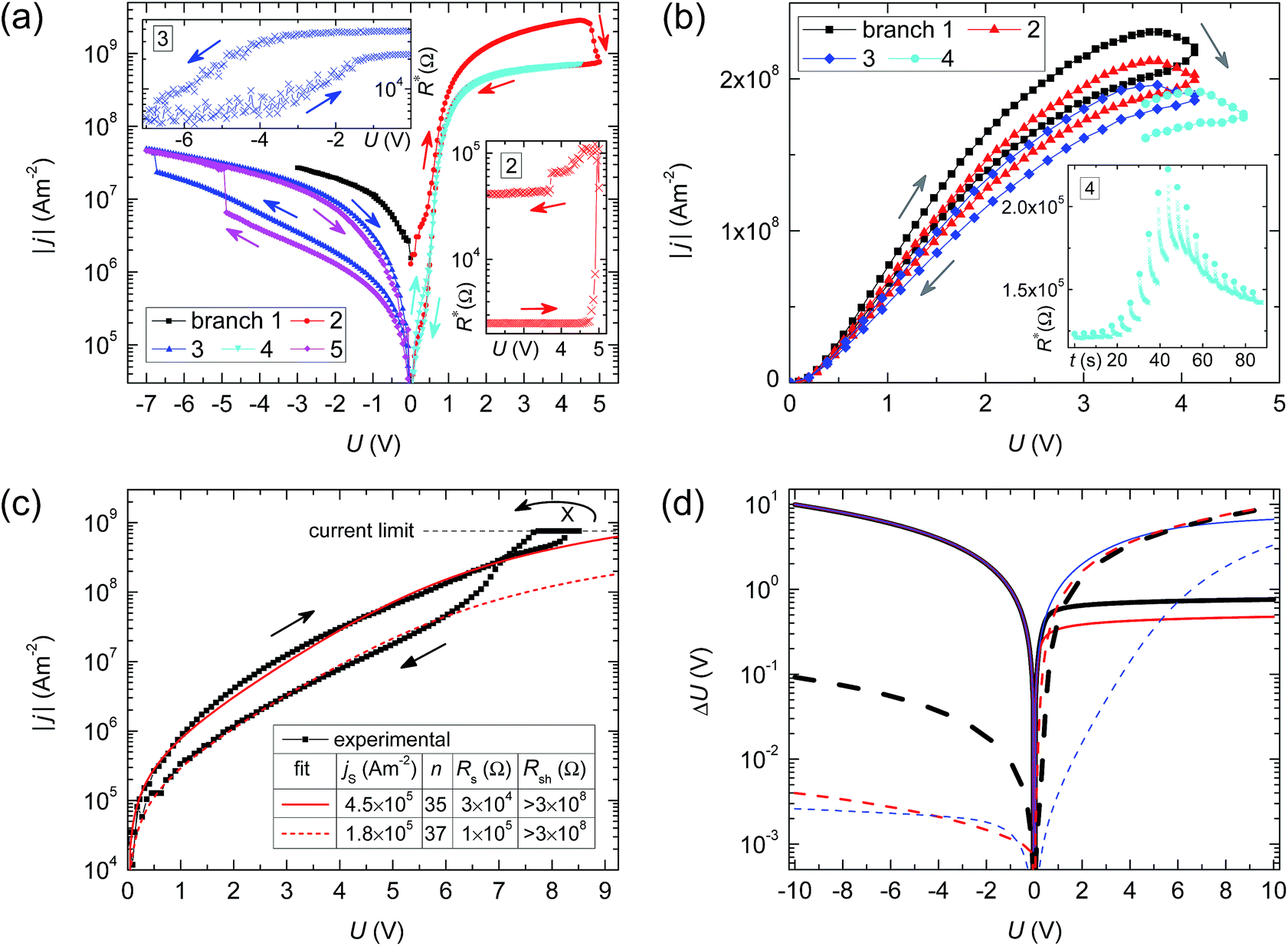
Fig. 3(a) shows the typical resistive switching properties of a pad-sample. At a forward bias U ≈ 4 V and currents j ≳ 3 × 10⁹ Am−2, the current–voltage characteristics undergo pronounced remanent changes as quantified by the equivalent-circuit model analysis: Rs (Rsh) increases by up to a factor of 3 (20), jS decreases to the order of 103 Am−2 while the ideality factor is basically unaffected. Under reverse bias U ≳ 4 V, jS increases by a factor of 2–5, thus only partially recovering its virgin level, and Rsh switches back down though always remaining above its initial value. Reverse biasing does not affect Rs as revealed in the subsequent forward branch (branch 4 in the figure): the high-resistive characteristic at high bias is accurately retraced while only the low-bias region, which is limited by the currents flowing through diode and shunt resistance, exhibits hysteresis. The evolution of the low-bias resistance R* in branch 2 reveals that the changes in the pn junction characteristics emerge simultaneously with the HRS formation in Rs. More extensive EPIR data is provided as ESI-Fig. 4.† Therein, successive current–voltage cycles further increases the low-bias resistance, eventually reaching stable HRS and LRS levels, see (c). After the initial HRS formation in Rs, its value remains unaffected by the repeated cycling within the given voltage regime (application of higher voltages soon yields sample failure, see below).Determining factors for resistive switching are electric field, electric current and Joule heating. In order to estimate the former, we plot the fractional voltage drop across the series resistance ΔU(Rs) = Rs·I and across the pn junction ΔU(diode) = ΔU(Rsh) = U − ΔU(Rs) for our equivalent circuit with different parameter settings in Fig. 3(d). Finite element simulations of the temperature evolution in our pad-samples under electric pulses predict significant local heating only for current densities j > 1 × 10⁹ Am−2, e.g. a temperature increase by ∼300 K at 5 × 10⁹ Am−2.51 This is consistent with our experimental observation of fatal sample failure by crack formation and local melting of the photo-resist layer in this current regime. Altogether, the HRS formation of the series resistance at high forward bias occurs under the combined action of a large voltage drop, high current density and rather massive Joule heating. Under reverse bias neither of these quantities acts comparably strong on Rs, which consequently remains unchanged. In contrast, reverse biasing yields a nearly complete voltage drop across the pn junction. The emerging electric fields (on the order of ∼108 Vm−1 as stated above) are apparently sufficient to counteract the foregoing forward bias switch and partially recover jS and Rsh towards their initial values.
The low-bias resistance in between the ”pump” pulses displays temporal relaxation behaviour on both forward and reverse bias branches (see insets in Fig. 3(a)). Based on the respective current density levels, only the relaxation on the forward branch can be assigned to Joule heat dissipation, while no significant temperature increase is expected under reverse bias.‡ As will be discussed later, we interprete this finding as evidence for relaxation of an oxygen vacancy distribution driven out of equilibrium.
Given the aforementioned limitations imposed by the surface contributions in TEM-samples, the in situ TEM investigations of the EPIR are restricted to the effects accompanying the HRS formation in Rs. Especially, changes of the pn junction shunt resistance can hardly be observed, since the reverse bias branch as well as the low-bias regime of the forward branch are dominated by the parasitic contributions of the surface states. Although we are thus restricted to the analysis of the forward bias branches, we verified that reverse biasing does not affect Rs, consistent with the findings in pad-samples. Furthermore, the differences in thermal coupling, i.e. the much lower heat conductivity compared to pad-samples due to the surfaces with vacuum, lowers the threshold current for TEM-sample failure by approximately one order of magnitude to j ≳ 5 × 10⁸ Am−2.
Fig. 3(b) shows the HRS formation in a thick TEM-sample. The successive forward biasing eventually increases Rs by a factor of ∼2 compared to the initial state. The TEM-sample has a low ideality factor n ≈ 2 and therefore the fractional voltage drop across its equivalent-circuit components corresponds to the relations in pad-samples (see Fig. 3(d)). The relative increase of Rs as well as the switching voltage U ≈ 4 V closely resemble the observations in pad-samples. However, the current density during resistive switching is about one order of magnitude lower. Given the reduced heat conductivity of the TEM-samples, this finding suggests that Joule heating plays a major role for the HRS formation. The relaxation of the low-bias resistance in the inset of Fig. 3(b) follows an exponential decay R*(t) ∝ exp(−t/τ) with τ ≈ 1 s, which equals the corresponding time constants found for pad-samples (not shown). Likewise, we consider this relaxation behaviour in the EPIR regime in part as due to Joule heat dissipation, but possibly also as the fingerprint of the equilibration of a highly driven state, which is characterized by the onset of oxygen vacancy electromigration and unbalanced charge carrier exchange rates (see below).§
Fig. 3(c) shows resistive switching in a thin TEM-sample, whose high ideality factor allows for proper fitting of changes in the diode parameters. Due to the lower fractional voltage drop across the series resistance, the current respectively heating level for switching is only reached at U > 8 V. Irregular behaviour at high forward bias, as displayed in this viewgraph, is occasionally observed within the narrow current regime between switching and sample failure (cf. section 4).
In comparison with pad-samples, the HRS formation in Rs is well reproduced in TEM-samples. In both types of samples, Rs increases at sufficient forward bias by a factor of up to 3, while it is unaffected by reverse biasing. The current density during switching is in each case close to the respective sample-failure threshold indicating the presence of similar levels of Joule heating. Concerning the equivalent-circuit model parameters of the very pn junction, only the initial decrease of IS accompanying the HRS formation in Rs is evident in TEM-samples, while switching of the intrinsic Rsh as well as the rather subtle changes associated with repeated reverse biasing remain hidden behind the parasitic contributions of the surface states.
4 Microstructural changes accompanying resistive switching
The TEM investigations of microstructural changes during resistive switching are capable of addressing the different elements of the equivalent-circuit individually, i.e. the interfacial region around the pn junction, governing the diode characteristics and Rsh, and the PCMO film and its interface to the Au electrode jointly constituting Rs.Fig. 4 shows the results of EFTEM/EELS investigations of the oxygen K edge before and after electric-pulse induced resistive switching of a TEM-sample. The electrical stimulation with a pulsed forward bias loop led to HRS formation, namely a doubling of Rs and a decrease of jS by a factor of ∼5 as determined by the fits (see inset of (c)). Despite the low signal-to-noise ratio in the EFTEM data, subfigures (a)–(c) reveal a subtle but regularly observed peculiarity in the elemental oxygen distribution, namely an oxidation of the STNO by high forward currents in an initially oxygen-depleted region below the interface to the PCMO film, extending ∼50 nm into the substrate (shaded area in (c); see ESI-Fig. 4† for another example). Although Fig. 4(c) may indicate an apparent global oxygen uptake, this was not systematically observed throughout our experiments, in particular not for the PCMO film area. Furthermore, EFTEM elemental maps of the cations are unaffected by electrical stimulation.
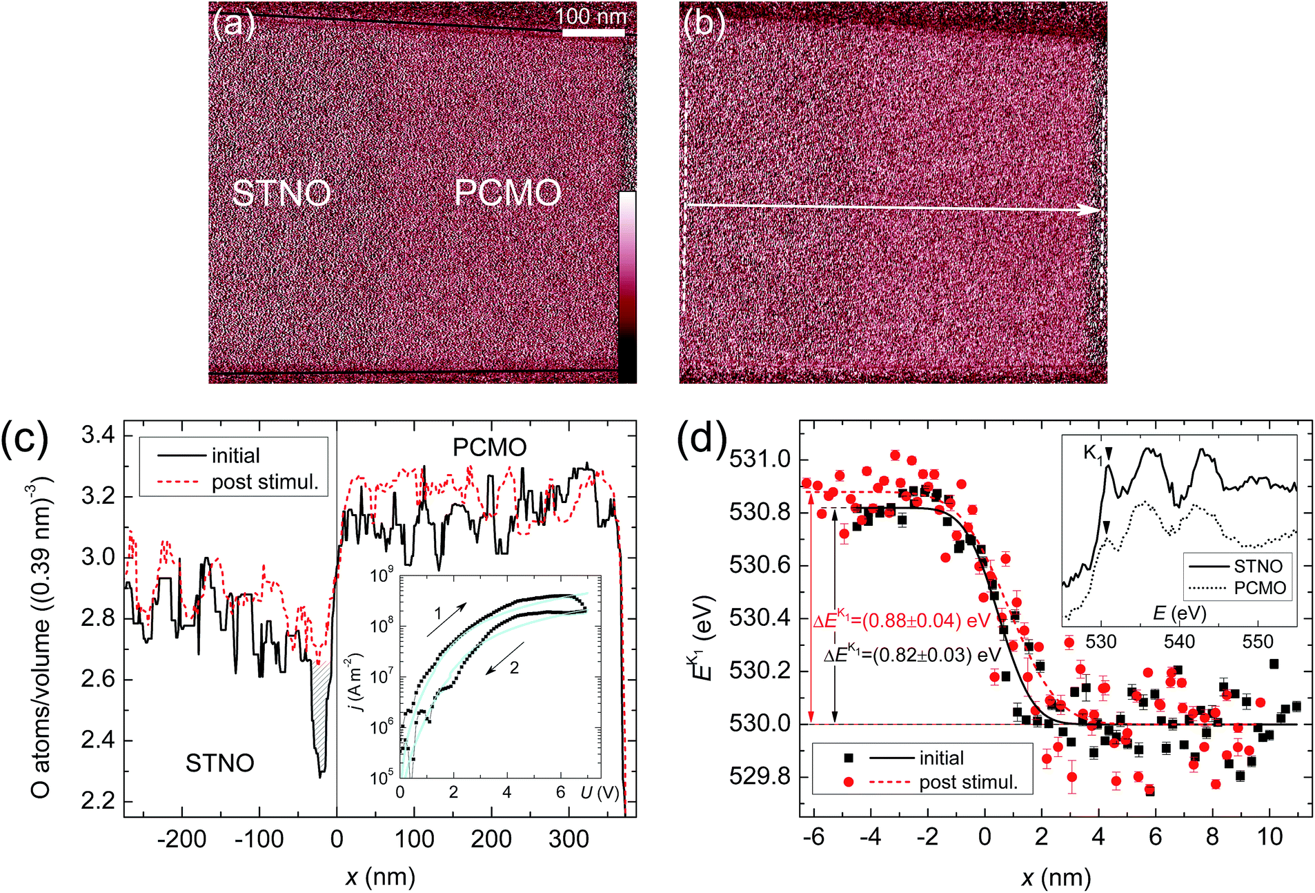 | ||
| Fig. 4 Elemental oxygen maps and O K ELNES evolution across the PCMO/STNO junction. False-color maps of atomic volume density from EFTEM (a) before and (b) after electric-pulse induced HRS formation. The black lines in (a) mark the TEM-sample contour. (c) Averaged line profiles from areas as indicated in (b), x = 0 corresponds to the position of the junction. The profiles are additionally smoothed by a median filter of 15 nm width. (See ESI† for a comment on the accuracy of the absolute values). Inset: in situ current–voltage curve (symbols) and corresponding fits (lines); the map in (b) was acquired after this stimulus. Fit parameters on branch 1(2) are jS = 5(1) × 105 Am−2, n = 13(13), Rs = 2.5(5) × 105 Ω and Rsh ≈ 1(1) × 108 Ω. (d) Evolution of the peak center of O K ELNES feature K1 across the junction. Symbols are determined from individual spectra in line scans (see ESI†), lines are corresponding error function fits. Data is offset to a joint energy level in PCMO. Inset: O K ELNES in the bulk materials. | ||
The observation of an oxygen-deficient STNO surface zone in pristine TEM-samples is rather surprising, since oxygen concentration-cell experiments suggest equilibrium vacancy concentrations only on the order of 1019–1020 cm−3 under our deposition conditions.52 Additional vacancies are possibly introduced by gettering effects of the PCMO overlayer,53–55 or by the irradiation during FIB processing.
Nevertheless, the observed electromigration of vacancies under forward biasing is reasonable on the basis of diffusive transport data reported in the literature. For the diffusion of (preexisting) oxygen vacancies in STO single crystals, an activation energy EA = 0.26 eV and a diffusion constant D0 = 1.3 × 10⁻⁵ cm2 s−1 are reported,56 consistent with a diffusion coefficient D(T = 500 K) ≈ 2 × 10⁻⁸ cm2 s−1 in ref. 57. According to the Huntington–Grone theory,58 the vacancy drift velocity in the presence of an applied electric field E equals v = DZ*eE/kBT, wherein we set the effective charge of the oxygen vacancies to Z* = +2. For the parameter regime of the resistive switching in the TEM-samples, i.e. T = 400–600 K and E = j·ρSTNO with j = 2 × 10⁸ Am−2 and ρSTNO (T) = (0.5–1) × 10−3 Ωm, this yields a coarse estimate of the oxygen vacancy diffusion lengths Δx = tpv ≈ 10–100 nm within our electric pulses of tp = 2 ms duration.
The analysis of the electron-loss near-edge structure (ELNES) of the oxygen K edge in Fig. 4(d) provides detailed information about the electronic structure of the pn junction and its changes by the electrical stimulation. The O K edge (1s → 2p transition) probes the unoccupied states above the Fermi level and can be interpreted as the site- and symmetry-projected density-of-states given the strong screening of the remaining core-hole.59 The first ELNES feature (labelled K1) arises from covalent mixing of O 2p with the transition metal 3d states and represents the bottom of the respective conduction bands.60–62 The conduction band offset  across the junction determines the reverse barrier ϕb for electrons from the PCMO side carrying the reverse saturation current, IS ∝ exp(−ϕb/kBT). The slight increase
 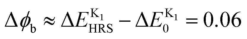 eV in the HRS after oxidation of the STNO interfacial region by the electrical stimulation corresponds to a concomitant decrease of the saturation current IS,HRS/IS,0 = exp(−Δϕb/kBT) ≈ 0.1 at room temperature. This value is in line with the regularly observed switch of IS by an order of magnitude in the current–voltage curves of both TEM- and pad-samples. Likewise, an increase of ϕb by oxidation of the SrTiO3 interfacial region was also predicted by Jeon et al. for Schottky junctions of SrTiO3 with SrRuO3.63
The reduction of the n-doping level in the interfacial STNO by the loss of oxygen vacancies also accounts for the increase of Rsh observed in pad-samples: due to the corresponding widening of the depletion layer, the underlying band-to-band-tunneling across the junction suffers from a reduction of the built-in electric field (or an increase of the effective tunneling length respectively).
Reverse biasing of TEM-samples leaves no visible effects in EFTEM elemental maps or EELS spectra. Given the low current level in the reverse regime, any change in the oxygen vacancy distribution accompanying the partial recovery of IS and Rsh towards their initial values is supposed to take place in the narrow region of high electric field around the junction, but cannot be resolved in our experiments. At least, we argue that the resistance creep observed in the backward scan (−Umax → 0) of reverse bias branches in pad-samples (see top inset of Fig. 3(a)) is an indication of a slow oxygen vacancy redistribution.
The HRS formation in Rs is not reflected by any spectroscopically detected changes at the interface between PCMO and Au top electrode. The very interface consists of a ∼2 nm wide amorphous PCMO layer with an increased oxygen/cation atomic ratio of ∼3 compared to 3/2 in bulk PCMO (see ESI-Fig. 5†). Width and stoichiometry of this layer as well as O K and Mn L ELNES in the interfacial region are unaffected by both forward and reverse biasing. We find no evidence for an electrochemical redox mechanism involving the Au top electrode as proposed for the resistive switching of interfaces between PCMO and various less noble metal electrodes.10,11,13,64 The anodic oxidation of the Au electrode under forward bias is supposed to be energetically hindered by the high standard enthalpy of formation for Au-oxide (ΔH0f = −13 kJ mol−1 or even > +100 kJ mol−1 for Au2O3,65,66 compared to −80 kJ mol−1 for PtO2,67 and the oxides of less noble metals widely discussed for the formation of interfacial oxide layers, e.g. WO2 −590 kJ mol−1, TiO2 −945 kJ mol−1 or Al2O3 −1676 kJ mol−1 (ref. 68)). Under reverse bias the driving force for oxygen migration out of the interfacial region is insignificant given the minor fractional voltage drop across the PCMO/Au interface (remind of Fig. 3(d)). Consistent with our findings, also Li et al. and Kim et al. report no evidence for anodic oxidation of Au electrodes in the switching regime of PCMO-based samples.14,64
The HRS formation in Rs is therefore ascribed to changes within the PCMO film. Resistive switching of bulk PCMO in addition to interface effects was also reported from scanning Kelvin probe measurements of a switching device between laterally arranged electrodes.21 As stated above, the oxygen distributions in the PCMO films as revealed in our EFTEM experiments exhibit no systematic changes by the electrical stimulation. Literature data for oxygen vacancy diffusion in hole-doped manganites yield higher activation energies compared to STO, namely EA = 0.4–1.3 eV.16,69,70¶ Due to the corresponding shorter diffusion length as well as the lower vacancy concentration compared to the oxygen-depleted STNO surface layer, any electromigrative redistribution is supposed to take place below the EFTEM detection limit. However, evidence for a major contribution of oxygen vacancy migration to the HRS formation in Rs is provided by the electrical transport data. Comparing current–voltage curves and intermediate pulses, we always observe that the HRS formation in both Rs and the pn junction occurs simultaneously – see e.g. branch 2 in Fig. 3(a), where the current drop at U > 4.5 V, representing the HRS formation in Rs, is accompanied by a simultaneous increase of the low-bias resistance, which is entirely dominated by the junction parameters (remind of ESI-Fig. 2†) and caused by the electromigrative oxidation of the STNO side of the junction as shown in the previous paragraph. We attribute this coincidence to a global temperature increase by Joule heating crossing a threshold value for thermally activated electromigration of oxygen vacancies. The concentration of oxygen vacancies is a key parameter controlling the transport properties of manganites, especially since they act as electron donors and thus significantly affect the delicate balance between itineracy and localization tendencies in Mn 3d states. It was recently shown, e.g., that oxygen vacancies in PCMO can induce local Mott gaps, mimicking the electronic structure of the undoped, insulating parent compound PrMnO3.18 Taking into account the qualitative picture of these correlation physics by a double-exchange Hamiltonian, Quintero et al. found indeed that subtle oxygen vacancy redistributions between bulk and interfacial region can account for the resistive switching properties observed in Pr0.3La0.075Ca0.325MnO3 films.72 An in situ TEM observation of oxygen vacancy migration in PCMO under a steady electric field of ∼9 × 10⁶ Vm−1 was reported by Liao et al.17 This value corresponds to the field strength across the PCMO films applied in the EPIR regime of our samples.||
Another source for doping level modulations are the differences of the charge carrier mobilities in the involved materials, namely small hole polarons with thermally activated hopping transport properties in PCMO,73 and (quasi-)free conduction band electrons in STNO and Au, respectively. It has been pointed out by Emin that the electrical transport under such circumstances is governed by the low intersite hopping rate of the small polarons and especially by the supposedly even lower rate of conversion between quasifree and polaron carriers at the interfaces to the electrodes.74 Likewise, the domain model of Rozenberg et al. with two distinguished carrier transfer rates between electrode and interface domains as well as between interface and bulk domains captures the salient features of bipolar, nonvolatile memory devices.75,76 Emin predicted ibid. that a driven non-equilibrium state with a strongly inhomogeneous polaron density could result in a dynamic destabilization of the polarons into a highly conductive state that in turn couples to the lattice and eventually induces a structural phase transition. Our in situ TEM measurements indeed yield experimental evidence for such a process during the HRS formation, see Fig. 5. Therein, the in situ recorded SAD patterns reveal a dynamic change of the PCMO twin system, namely a transformation of the initial [100] zone axis in subfigure (a) to a dominant [010] orientation with only minor remnants of the pristine twin in (b). The transition between the twins equals subtle tiltings of the MnO6 octahedra within the orthorhombic Pbnm structure (space group no. 62).77 The vibrational patterns of the MnO6 octahedra constitute the relevant phonon modes of the small polaron formation in PCMO.78–80 Highly driven polaron states can thus give rise to strong excitations of the octahedral tilt system, which in combination with Joule heating can induce changes in the twin system. We observe this transformation frequently under high forward currents on the order of 108 Am−2, i.e. in the EPIR regime. The highly irregular shape of the corresponding current–voltage curve in Fig. 3(c) with an intermediately augmented conductivity is a rather extreme example of the nonlinear characteristics that sometimes, but not always, accompany the twin transformation. Such irregularities are also found in pad-samples, but only at one-order-of-magnitude higher current densities, which indicates that Joule heating is an important contributor (remind of the different heat conductivities of TEM- and pad-samples).
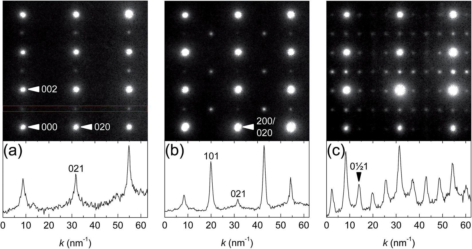 | ||
| Fig. 5 Superstructure formation in PCMO during resistive switching. Top panels: in situ SAD patterns of the PCMO film (projected aperture diameter 300 nm) at different stages of the current–voltage curve displayed in Fig. 3(c). Bottom panels: averaged line profiles from regions as marked by the red rectangle in (a). (a) Virgin pattern on the initial branch. (b) Intermediate pattern (duration ∼250 ms, i.e. 5 pulses) emerging at the onset of resistive switching marked by the cross in Fig. 3(c). (c) Persistent final pattern on the backward branch following the pattern in (b). | ||
In addition to the frequently observed twin transformation, the HRS formation is sometimes accompanied by a further structural phase transition as displayed in Fig. 5(c) (see ESI-Fig. 6† for another example). Based on the TEM investigations, this structure is reminiscent to the charge- and orbital-ordered, low-temperature P21nm phase of PCMO (space group no. 31) with a real-space doubling of the unit cell in the crystallographic b-direction.78 We already reported such electrically induced superstructure formation for PCMO bulk samples.24 In TEM-samples, superstructure domains are found to nucleate at both interfaces to STNO and Au respectively and sometimes even spread across the whole PCMO film in a filamentary manner. The P21nm phase is characterized by the long-range ordering of Zener polarons on specific lattice sites with a nominal density of 0.5 holes per pseudo-cubic unit cell, which is higher than the average density in PCMO with x = 0.35 Ca doping. We thus argue that the electrically induced superstructure formation is a means of accommodating an inhomogeneous carrier density, which occurs in the EPIR regime by the combined impact of oxygen vacancy electromigration and high-mobility carrier injection/extraction at the electrodes.
5 Conclusions
Resistive switching in Au/PCMO/STNO thin-film heterostructures was studied by means of in situ TEM and equivalent-circuit model analysis. The electrical transport properties of both electron-transparent cross-section samples used for in situ TEM and unpatterned reference samples prove to be basically identical, namely rectifying current–voltage characteristics due to the PCMO/STNO pn junction with forward currents being limited by the series resistance of the manganite film and its interface to the Au top electrode. Under sufficient forward currents and a corresponding Joule heating level, a nonvolatile high-resistance state is formed in the PCMO film evident as an increase of the series resistance. Simultaneously, the reverse saturation current across the pn junction as well as its shunt resistance decreases and increases, respectively. The built-in asymmetry of the current–voltage characteristics with respect to the voltage polarity entails that only these junction related resistive switching effects can be reversed under reverse bias, since the only action in this regime is imparted by the voltage drop across the pn junction. The in situ TEM investigations revealed that the resistive switching of the pn junction under forward bias is accompanied by an electromigrative oxidation of an initially oxygen-depleted surface layer in the STNO, gradually increasing the height of the junction potential barrier which represents the underlying reason for the change of the junction parameters. In contrast, the high-resistance state formation in the series resistance is not reflected by microstructural or chemical changes of the interface with the top electrode, in particular, no anodic oxidation of the Au was observed. Instead, we frequently observed a detwinning of the epitaxial PCMO microstructure as well as a structural transition to a long-range ordered phase reminiscent of the insulating ground state of PCMO. These findings indicate that changes within the bulk PCMO film contribute to the resistive switching, in contrast to the interface-dominated switching in devices with non-noble metal electrodes. We argue that the fundamental impetus underlying these modifications stems from electronic inhomogenities, which are imposed by electromigrative oxygen vacancy redistribution as well as by non-equilibrium charge carrier exchange rates between PCMO and the electrodes.Acknowledgements
We thank H. Hofsäss (II. Phys. Institut, Universität Göttingen) for the MC simulations of the irradiation damages induced by FIB sample preparation. Funding by the Deutsche Forschungsgemeinschaft (DFG) under grant numbers JO 348/10-1 and SFB1073 is acknowledged.References
- S. Q. Liu, N. J. Wu and A. Ignatiev, Appl. Phys. Lett., 2000, 76, 2749 CrossRef CAS PubMed.
- A. Sawa, Mater. Today, 2008, 11, 28 CrossRef CAS.
- Y. Chen, L. Chen, G. Lian and G. Xiong, J. Appl. Phys., 2009, 106, 023708 CrossRef PubMed.
- W. W. Zhuang, W. Pan, B. D. Ulrich, J. J. Lee, L. Stecker, A. Burmaster, D. R. Evans, S. T. Hsu, M. Tajiri, A. Shimaoka, K. Inoue, T. Naka, N. Awaya, A. Sakiyama, Y. Wang, S. Q. Liu, N. J. Wu and A. Ignatiev, Int. Electron Devices Meet., 2002, 193 CAS.
- R. Waser, R. Dittmann, G. Staikov and K. Szot, Adv. Mater., 2009, 21, 2632 CrossRef CAS.
- H. Akinaga and H. Shima, Proc. IEEE, 2010, 98, 2237 CrossRef CAS.
- Y. Fujisaki, Jpn. J. Appl. Phys., 2013, 52, 040001 CrossRef.
- Z. Liu, P. Zhang, Y. Meng, H. Tian, J. Li, X. Pan, X. Liang, D. Chen and H. Zhao, Appl. Phys. Lett., 2012, 100, 143506 CrossRef PubMed.
- K. Tsubouchi, I. Ohkubo, H. Kumigashira, M. Oshima, Y. Matsumoto, K. Itaka, T. Ohnishi, M. Lippmaa and H. Koinuma, Adv. Mater., 2007, 19, 1711 CrossRef CAS.
- S. Asanuma, H. Akoh, H. Yamada and A. Sawa, Phys. Rev. B: Condens. Matter Mater. Phys., 2009, 80, 235113 CrossRef.
- K. Shono, H. Kawano, T. Yokota and M. Gomi, Applied Physics Express, 2008, 1, 055002 CrossRef.
- Z. L. Liao, Z. Z. Wang, Y. Meng, Z. Y. Liu, P. Gao, J. L. Gang, H. W. Zhao, X. J. Liang, X. D. Bai and D. M. Chen, Appl. Phys. Lett., 2009, 94, 253503 CrossRef PubMed.
- F. Borgatti, C. Park, A. Herpers, F. Offi, R. Egoavil, Y. Yamashita, A. Yang, M. Kobata, K. Kobayashi, J. Verbeeck, G. Panaccione and R. Dittmann, Nanoscale, 2013, 5, 3954 RSC.
- D. S. Kim, Y. H. Kim, C. E. Lee and Y. T. Kim, Phys. Rev. B: Condens. Matter Mater. Phys., 2006, 74, 174430 CrossRef.
- M. Scherff, B.-U. Meyer, J. Hoffmann and C. Jooss, J. Appl. Phys., 2011, 110, 043718 CrossRef PubMed.
- Y. B. Nian, J. Strozier, N. J. Wu, X. Chen and A. Ignatiev, Phys. Rev. Lett., 2007, 98, 146403 CrossRef CAS.
- Z. Liao, P. Gao, X. Bai, D. Chen and J. Zhang, J. Appl. Phys., 2012, 111, 114506 CrossRef PubMed.
- H. S. Lee, S. G. Choi, H.-H. Park and M. J. Rozenberg, Sci. Rep., 2013, 3, 1704 Search PubMed.
- S. T. Hsu, T. Li and N. Awaya, J. Appl. Phys., 2007, 101, 024517 CrossRef PubMed.
- C. Jooss, J. Hoffmann, J. Fladerer, M. Ehrhardt, T. Beetz, L. Wu and Y. Zhu, Phys. Rev. B: Condens. Matter Mater. Phys., 2008, 77, 132409 CrossRef.
- X. Chen, N. J. Wu, J. Strozier and A. Ignatiev, Appl. Phys. Lett., 2005, 87, 233506 CrossRef PubMed.
- P. Gao, Z. Wang, W. Fu, Z. Liao, K. Liu, W. Wang, X. Bai and E. Wang, Micron, 2010, 41, 301 CrossRef CAS PubMed.
- S.-J. Choi, G.-S. Park, K.-H. Kim, W.-Y. Yang, H.-J. Bae, K.-J. Lee, H. i. Lee, S. Y. Park, S. Heo, H.-J. Shin, S. Lee and S. Cho, J. Appl. Phys., 2011, 110, 056106 CrossRef PubMed.
- C. Jooss, L. Wu, T. Beetz, R. F. Klie, M. Beleggia, M. A. Schofield, S. Schramm, J. Hoffmann and Y. Zhu, Proc. Natl. Acad. Sci. U. S. A., 2007, 104, 13597 CrossRef CAS PubMed.
- L. J. Zeng, H. X. Yang, Y. Zhang, H. F. Tian, C. Ma, Y. B. Qin, Y. G. Zhao and J. Q. Li, Europhys. Lett., 2008, 84, 57011 CrossRef.
- D.-H. Kwon, K. M. Kim, J. H. Jang, J. M. Jeon, M. H. Lee, G. H. Kim, X.-S. Li, G.-S. Park, B. Lee, S. Han, M. Kim and C. S. Hwang, Nat. Nanotechnol., 2010, 5, 148 CrossRef CAS PubMed.
- A. Sawa, T. Fujii, M. Kawasaki and Y. Tokura, Appl. Phys. Lett., 2005, 86, 112508 CrossRef PubMed.
- G. Saucke, J. Norpoth, C. Jooss, D. Su and Y. Zhu, Phys. Rev. B: Condens. Matter Mater. Phys., 2012, 85, 165315 CrossRef.
- L. Xia, W. Wu, Y. Hao, Y. Wang and J. Xu, Appl. Phys. Lett., 2006, 88, 152108 CrossRef PubMed.
- P. Moschkau, S. Schramm, J. Hoffmann, J. Fladerer, C. Jooss, L. Wu and Y. Zhu, Mater. Sci. Eng., B, 2007, 144, 78 CrossRef CAS PubMed.
- M. Scherff, J. Hoffmann, B. Meyer, T. Danz and C. Jooss, New J. Phys., 2013, 15, 103008 CrossRef.
- O. Breitenstein, J. P. Rakotoniaina, M. H. Al Rifai and M. Werner, Prog. Photovoltaics, 2004, 12, 529 CAS.
- Y. Taur and T. H. Ning, Fundamentals of Modern VLSI Devices, Cambridge University Press, 2nd edn., 2009, pp. 125–126 Search PubMed.
- P. M. Solomon, J. Jopling, D. J. Frank, C. D'Emic, O. Dokumaci, P. Ronsheim and W. E. Haensch, J. Appl. Phys., 2004, 95, 5800 CrossRef CAS PubMed.
- K. J. B. M. Nieuwesteeg, M. van der Veen, T. J. Vink and J. M. Shannon, J. Appl. Phys., 1993, 74, 2581 CrossRef CAS PubMed.
- W. Shockley and W. T. Read, Phys. Rev., 1952, 87, 835 CrossRef CAS.
- C. Sah, R. N. Noyce and W. Shockley, Proc. IRE, 1957, 45, 1228 CrossRef.
- A. Schenk and U. Krumbein, J. Appl. Phys., 1995, 78, 3185 CrossRef CAS PubMed.
- U. Rau, Appl. Phys. Lett., 1999, 74, 111 CrossRef CAS PubMed.
- V. Nadenau, U. Rau, A. Jasenek and H. W. Schock, J. Appl. Phys., 2000, 87, 584 CrossRef CAS PubMed.
- A. R. Riben and D. L. Feucht, Int. J. Electron., 1966, 20, 583 CrossRef CAS.
- M. Brötzmann, U. Vetter and H. Hofsäss, J. Appl. Phys., 2009, 106, 063704 CrossRef PubMed.
- H. Hofsäss (II. Physikalisches Institut Universität Göttingen), Private communication. The simulations are performed with the SDTrimSP software (Eckstein et al., MPI for Plasma Physics - IPP Report12/8, 2011) and take into account the precise geometry of the FIB preparation process.
- E. Montoya, S. Bals, M. D. Rossell, D. Schryvers and G. Van Tendeloo, Microsc. Res. Tech., 2007, 70, 1060 CrossRef CAS PubMed.
- N. I. Kato, J. Electron Microsc., 2004, 53, 451 CrossRef CAS.
- Y. Yabuuchi, S. Tametou, T. Okano, S. Inazato, S. Sadayama, Y. Yamamoto, K. Iwasaki and Y. Sugiyama, J. Electron Microsc., 2004, 53, 471 CrossRef CAS.
- S. Dong, R. Yu, S. Yunoki, J.-M. Liu and E. Dagotto, Phys. Rev. B: Condens. Matter Mater. Phys., 2008, 78, 064414 CrossRef.
- S. S. Rao, S. Tripathi, D. Pandey and S. V. Bhat, Phys. Rev. B: Condens. Matter Mater. Phys., 2006, 74, 144416 CrossRef.
- C. L. Lu, S. Dong, K. F. Wang, F. Gao, P. L. Li, L. Y. Lv and J.-M. Liu, Appl. Phys. Lett., 2007, 91, 032502 CrossRef PubMed.
- A. Sadhu, T. Kramer, A. Datta, S. A. Wiedigen, J. Norpoth, C. Jooss and S. Bhattacharyya, Chem. Mater., 2012, 24, 3758 CrossRef CAS.
- M. Feuchter and M. Kamlah, (Forschungszentrum Karlsruhe), Private communication. Details will be published elsewhere.
- I. Denk, W. Münch and J. Maier, J. Am. Ceram. Soc., 1995, 78, 3265 CrossRef CAS PubMed.
- V. A. Gasparov, S. N. Ermolov, G. K. Strukova, N. S. Sidorov, S. S. Khassanov, H.-S. Wang, M. Schneider, E. Glaser and W. Richter, Phys. Rev. B: Condens. Matter Mater. Phys., 2001, 63, 174512 CrossRef.
- K. S. Takahashi and H. Y. Hwang, Appl. Phys. Lett., 2008, 93, 082112 CrossRef PubMed.
- J. D. Ferguson, Y. Kim, L. Fitting Kourkoutis, A. Vodnick, A. R. Woll, D. A. Muller and J. D. Brock, Adv. Mater., 2011, 23, 1226 CrossRef CAS PubMed.
- L. C. Walters and R. E. Grace, J. Phys. Chem. Solids, 1967, 28, 245 CrossRef CAS.
- R. Waser, T. Baiatu and K.-H. Härdtl, J. Am. Ceram. Soc., 1990, 73, 1654 CrossRef CAS PubMed.
- H. B. Huntington and A. R. Grone, J. Phys. Chem. Solids, 1961, 20, 76 CrossRef CAS.
- L. Fitting Kourkoutis, H. L. Xin, T. Higuchi, Y. Hotta, J. H. Lee, Y. Hikita, D. G. Schlom, H. Y. Hwang and D. A. Muller, Philos. Mag., 2010, 90, 4731 CrossRef.
- F. M. F. de Groot, M. Grioni, J. C. Fuggle, J. Ghijsen, G. A. Sawatzky and H. Petersen, Phys. Rev. B: Condens. Matter Mater. Phys., 1989, 40, 5715 CrossRef CAS.
- M. P. Kocher, D. A. Muller and P. Rez, Microsc. Microanal., 2003, 9(suppl. 02), 842 Search PubMed.
- M. Uijttewaal and P. E. Blöchl, (Technische Universität Clausthal), Private communication. The appropriate DFT calculations for PCMO based on the PBE0r functional will be published elsewhere.
- S. H. Jeon, B. H. Park, J. Lee, B. Lee and S. Han, Appl. Phys. Lett., 2006, 89, 042904 CrossRef PubMed.
- S.-L. Li, D. S. Shang, J. Li, J. L. Gang and D. N. Zheng, J. Appl. Phys., 2009, 105, 033710 CrossRef PubMed.
- S. J. Ashcroft and E. Schwarzmann, J. Chem. Soc., Faraday Trans. 1, 1972, 68, 1360 RSC.
- G. V. Samsonov, The Oxide Handbook, Plenum Press, 1st edn, 1973 Search PubMed.
- Y. Nagano, J. Therm. Anal. Calorim., 2002, 69, 831 CrossRef CAS.
- G. H. Aylward and T. J. V. Findlay, SI Chemical Data, John Wiley & Sons, 2nd edn, 1974 Search PubMed.
- T. Bak, J. Nowotny, M. Rekas, C. C. Sorrell and E. R. Vance, Solid State Ionics, 2000, 135, 557 CrossRef CAS.
- S. Carter, A. Selcuk, R. J. Chater, J. Kajda, J. A. Kilner and B. C. H. Steele, Solid State Ionics, 1992, 53–56, 597 CrossRef CAS.
- T. Ishigaki, S. Yamauchi, K. Kishio, J. Mizusaki and K. Fueki, J. Solid State Chem., 1988, 73, 179 CrossRef CAS.
- M. Quintero, P. Levy, A. G. Leyva and M. J. Rozenberg, Phys. Rev. Lett., 2007, 98, 116601 CrossRef CAS.
- S. Schramm, J. Hoffmann and C. Jooss, J. Phys.: Condens. Matter, 2008, 20, 395231 CrossRef.
- D. Emin, Phys. Rev. B: Condens. Matter Mater. Phys., 2006, 74, 035206 CrossRef.
- M. J. Rozenberg, I. H. Inoue and M. J. Sánchez, Phys. Rev. Lett., 2004, 92, 178302 CrossRef CAS.
- M. J. Rozenberg, I. H. Inoue and M. J. Sánchez, Appl. Phys. Lett., 2006, 88, 033510 CrossRef PubMed.
- Z. Jirák, S. Krupička, Z. Šimša, M. Dlouhá and S. Vratislav, J. Magn. Magn. Mater., 1985, 53, 153 CrossRef.
- L. Wu, R. F. Klie, Y. Zhu and C. Jooss, Phys. Rev. B: Condens. Matter Mater. Phys., 2007, 76, 174210 CrossRef.
- M. V. Abrashev, J. Bäckström, L. Börjesson, M. Pissas, N. Kolev and M. N. Iliev, Phys. Rev. B: Condens. Matter Mater. Phys., 2001, 64, 144429 CrossRef.
- V. Dediu, C. Ferdeghini, F. C. Matacotta, P. Nozar and G. Ruani, Phys. Rev. Lett., 2000, 84, 4489 CrossRef CAS.
Footnotes |
| † Electronic supplementary information (ESI) available. See DOI: 10.1039/c4nr02020k |
| ‡ We performed systematic measurements with multiple low-bias pulses following ”pump” forward bias pulses. Resistance relaxation effects were only found after pump pulses with j ≳ 1 × 10⁹ Am−2. They are ascribed to Joule heating, consistent with the results of the finite element simulations. |
| § The R* in Fig. 3(b) is measured at a higher forward bias than in (a) since the low-bias regime in the TEM-samples is dominated by the parasitic surface contributions. The interpretation of R* on the basis of the equivalent-circuit model is therefore not equally straightforward and has to deal not only with parameters related to the pn junction (IS, Rsh) but also with Rs. |
| ¶ The vacancy formation enthalpy has been subtracted from the self-diffusion data in ref. 70 based on the data provided in ref. 71. |
| || The reported slow vacancy drift velocity (∼10 nm in 100 s) seems to be not in line with the ms-timescale of our voltage-pulse experiments. We argue that this discrepancy is caused by different levels of Joule heating, since the electric current density during the stimulation is approximately two orders of magnitude higher in our experiments. |
| This journal is © The Royal Society of Chemistry 2014 |