 Open Access Article
 This Open Access Article is licensed under a
 Creative Commons Attribution 3.0 Unported Licence
Selective removal of metallic single-walled carbon nanotubes in full length by organic film-assisted electrical breakdown
Keigo
Otsuka
,
Taiki
Inoue
,
Shohei
Chiashi
* and
Shigeo
Maruyama
*
Department of Mechanical Engineering, The University of Tokyo, 7-3-1 Hongo, Bunkyo-ku, Tokyo 113-8656, Japan. E-mail: maruyama@photon.t.u-tokyo.ac.jp; chiashi@photon.t.u-tokyo.ac.jp; Fax: +81-3-5800-6983; Tel: +81-3-5841-6421
First published on 12th May 2014
Abstract
An organic film-assisted electrical breakdown technique is proposed to selectively remove metallic (m-) single-walled carbon nanotubes (SWNTs) in full length towards creation of pure semiconducting SWNT arrays which are available for the large-scale fabrication of field effect transistors (FETs). The electrical breakdown of horizontally aligned SWNT arrays embedded in organic films resulted in a maximum removal length of 16.4 μm. The removal of SWNTs was confirmed using scanning electron microscopy and Raman mapping measurements. The on/off ratios of FETs were improved up to ca. 10![[thin space (1/6-em)]](https://www.rsc.org/images/entities/char_2009.gif) 000, similar to that achieved for in-air breakdown. The experimental results suggest that exothermic oxidation of organic films induces propagation of oxidation reaction, hence the long-length removal of m-SWNTs.
000, similar to that achieved for in-air breakdown. The experimental results suggest that exothermic oxidation of organic films induces propagation of oxidation reaction, hence the long-length removal of m-SWNTs.
1 Introduction
High-density arrays of semiconducting (s-) single-walled carbon nanotubes (SWNTs) have potential for use in the channels of field-effect transistors (FETs) towards the realization of high-performance logic circuits.1,2 Although a further increase in the SWNT density is required, the horizontal growth of SWNTs with a high degree of alignment has been realized on crystal substrates.3–6 However, the as-grown SWNT array is a mixture of s- and metallic (m-) SWNTs, which is a major obstacle for FET fabrication using SWNTs, where pure s-SWNT arrays are required.7 Despite intensive efforts, the selective growth of s-SWNTs on substrates8–11 has not yet attained the required purity (m-SWNTs < 0.0001% (ref. 12)). Post-growth separation by wet chemical methods13–15 has provided ca. 99% purity of s-SWNT and dense, aligned arrays can be assembled after the separation.15–17 However, fabrication of high on/off ratio devices with sub-micrometer channel length requires higher purity, and the degree of alignment is needed to be improved. Post-growth removal of m-SWNTs from substrates2,18–22 has also been studied extensively. Electrical breakdown2,18 is one of the methods by which m-SWNTs are selectively cut by Joule heating, while the s-SWNTs are preserved through control of the gate voltage. Although electrical breakdown easily yields high on/off ratios for SWNT–FETs by exploiting the difference in the electric transport properties of m- and s-SWNTs, it has a major drawback in scalability. Basically individual FETs must be treated separately because only the hottest short parts (ca. 100 nm) of m-SWNTs are removed by oxidation, while most parts of the m-SWNTs remain after the process, as shown schematically in Fig. 1(a and b). If the full-length of m-SWNTs that bridge two electrodes could be completely removed, then this provides us with an alternative way for fabricating large numbers of FETs without one-by-one treatments. First, temporal electrodes with large widths and a large distance are fabricated on SWNT arrays only for a m-SWNT removing step, followed by performing a selective removal technique. After that, the remaining pure s-SWNT arrays between the temporal electrodes would be available for further fabrication of a large number of FETs by simply placing new electrodes and etching unwanted parts of s-SWNTs. The thermocapillary-induced full length removal technique22 recently proposed by Jin et al. is quite promising, even though the lateral spatial resolution is intrinsically limited by the capillary length scale.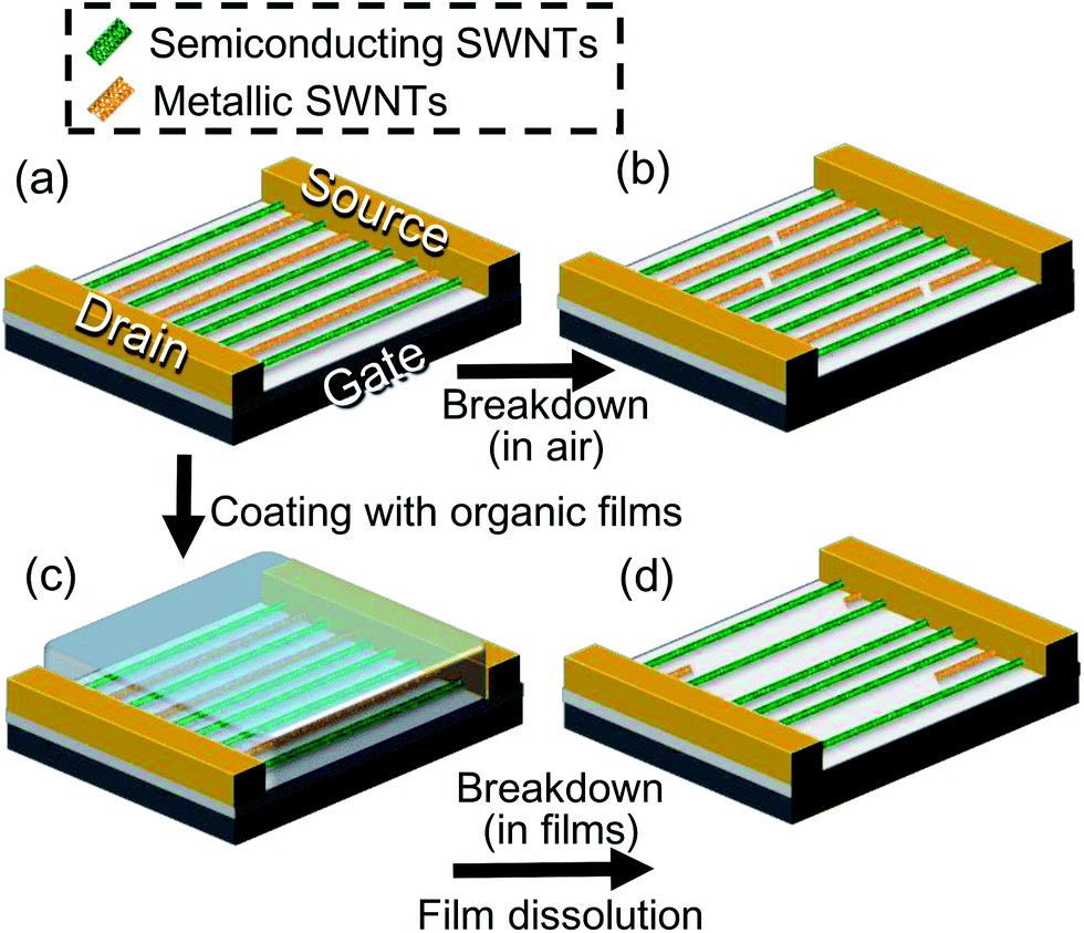 | ||
| Fig. 1 Schematic illustrations of (a and b) electrical breakdown in air and (a, c and d) electrical breakdown in organic films, respectively. Electrical breakdown in air on (a) an SWNT array with mixtures of s- and m-SWNTs results in (b) partial cutting of the m-SWNTs. In contrast, (c) electrical breakdown in organic films results in (d) the removal of m-SWNTs with longer lengths. The remaining s-SWNT arrays between the temporal electrodes can be used for further fabrication of a large number of FETs. | ||
In this work, an organic film-assisted electrical breakdown method has been developed to create pure s-SWNT arrays which can be used for a number of FET channels. Electrical breakdown was performed on SWNT arrays covered in organic films to accomplish the full-length removal of m-SWNTs (up to 16.4 μm). This method yielded a high on/off ratio (ca. 10000) of an FET, which indicates high removal selectivity between s- and m-SWNTs, and also showed fine spatial resolution (ca. 55 nm) in the same way as in-air breakdown.
2 Experimental section
Aligned arrays of SWNTs were grown by the alcohol catalytic chemical vapor deposition method23 on r-cut crystal quartz substrates.24,25 The SWNTs were then transferred onto highly p-doped Si substrates with a 100 nm-thick SiO2 layer.26 Source and drain electrodes were photolithographically defined to conduct currents through SWNTs using sputtering of 5 nm Ti and 50 nm Pd layers, which resulted in back-gated FET structures. FETs with channel widths of 20 μm and various channel lengths (2 to 30 μm) were fabricated. Only FETs with relatively low on/off ratios (less than 10) were used, which contained at least one m-SWNT bridging the source/drain electrodes.Schematic illustrations of organic film-assisted electrical breakdown are shown in Fig. 1(a, c, and d). For organic film-assisted electrical breakdown, SWNT arrays were coated with ca. 50 nm-thick organic films using thermal evaporation or spin-coating [Fig. 1(c)]. Two types of organic materials were utilized: α,α,α′-tris(4-hydroxyphenyl)-1-ethyl-4-isopropylbenzene (TCI), hereafter referred to as molecular glass, and poly(methyl methacrylate) (PMMA; Sigma-Aldrich, MW = ∼996000). The molecular glass is a small-molecule organic material that forms an amorphous thin film. The molecular glass was originally employed to reproduce the thermocapillary-induced process proposed by Jin et al.22 Through such experiments, a simpler technique with fine resolution was achieved using the organic films to enhance SWNT oxidation. In a typical experiment, the drain voltage (VD) was gradually increased from 0 V at a rate of ca. 0.67 V min−1 until the drain current (ID) became sufficiently small, while a positive gate voltage (VG = +10 V) was applied. This led to selective Joule heating in the m-SWNTs, which resulted in the breakdown of m-SWNTs. Finally, the organic films were removed by immersion of the substrates in acetone to give pure s-SWNT arrays [Fig. 1(d)].
Electrical breakdown and the transfer characteristics measurement of the FETs were performed under ambient conditions using a semiconductor parameter analyzer (Agilent 4156C). The SWNTs were characterized using scanning electron microscopy (SEM; Hitachi S-4800) with an accelerating voltage of 1 kV, atomic force microscopy (AFM; SII SPI3800N), and Raman mapping measurement (Renishaw inVia Raman microscope).
3 Results and discussion
Fig. 2(a and b) show SEM images of a part of an SWNT array before and after electrical breakdown in a molecular glass film, respectively. Fig. 2(c) shows the drain current transition during the breakdown process. Partial current drops correspond to the breakdown of SWNTs, and the number of drops is almost the same as the number of broken SWNTs observed with SEM. Among 29 SWNTs connected to both electrodes, 12 SWNTs were fully or partially removed, and this ratio (ca. 41%) is similar to the typical ratio of m-SWNTs in as-grown SWNTs (ca. 33%). The transfer characteristics of the FET before and after the breakdown process [Fig. 2(d)] show an increase in the on/off ratio from ca. 2 to 10000 and a decrease in the on-current by around 90%, which indicates that selective removal of the m-SWNTs was achieved. Although the removal lengths ranged from 1.4 to 16.4 μm, the entire length of the SWNT, indicated by the red arrows in Fig. 2(a and b), was removed. The removal length is over 100 times larger than that observed for conventional in-air breakdown (ca. 100 nm).
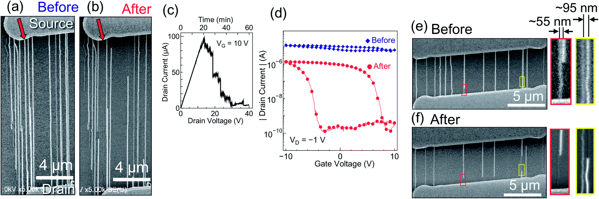 | ||
| Fig. 2 SEM images of an SWNT array (a) before and (b) after breakdown in molecular glass films. Red arrows indicate an m-SWNT that was removed over its full-length. (c) Drain current transition during the process, where the drain current dropped in accordance with the breakdown of SWNTs. (d) Transfer characteristics of the FET shown in (a and b), which indicate the selective breakdown of m-SWNTs. (e and f) SEM images of an SWNT array that contains closely-placed SWNTs. Close-up images of the outlined regions are insets in (e and f). In those cases, the breakdown of m-SWNTs did not affect adjacent SWNTs. | ||
Breakdown was performed on an SWNT array with close-lying SWNTs [Fig. 2(e)] to estimate the spatial resolution of organic film-assisted breakdown. The SWNT array shown in Fig. 2(f) was obtained; in the regions outlined by red and yellow lines, the distances between the removed m-SWNTs and the neighboring SWNTs were ca. 55 and 95 nm, respectively. The breakdown of m-SWNTs did not affect the neighboring SWNTs, which suggests that the spatial resolution of the breakdown is better than ca. 55 nm in the case of well-aligned SWNTs. Therefore, this method is potentially applicable to SWNT arrays with densities greater than ca. 18 SWNTs per μm. Considering that the thermocapillary-induced purification method yielded the minimum spacing of ca. 250 nm between two parallel and independent trenches22 and hence can be applied to SWNT arrays with densities up to ca. 8 SWNTs per μm, organic film-assisted electrical breakdown method can be more suitable for the fabrication of FETs with high current driving capability and small gate width.
Raman mapping measurements were performed to confirm the removal of SWNTs, using an excitation laser wavelength of 532 nm (the laser power density at the sample was ca. 4 × 10⁴ W cm−2). Fig. 3(a and b) show superimposed SEM and G-band mapping images of SWNTs before and after breakdown in a molecular glass film. White lines in the images represent SWNTs observed by SEM and green lines represent the areas from which G-band peaks were obtained. Fig. 3(c) shows the G-band and radial breathing mode (RBM) Raman spectra measured at the circled spots indicated in Fig. 3(a and b). The RBM peaks at 274 and 165 cm−1 were assigned as (9,3) chirality (metallic) and (14,7) chirality (semiconducting) under the excitation energy of 2.33 eV (532 nm),27 respectively. The Raman peaks obtained from the m-SWNT disappeared after breakdown. In this case, the s-SWNT was also removed unintentionally, because it happened to lie very close to the m-SWNT. The disappearance of the white lines from the SEM image and the green lines from the Raman mapping image is clearly consistent, which confirmed the long-length removal of the SWNTs. The Raman observations exclude the possibility of remaining SWNTs which are invisible with SEM due to residual organic materials surrounding the SWNTs or isolation from electron sources (metal electrodes).28 The power density of the excitation laser was low enough not to heat the SWNTs which directly touched the SiO2/Si substrates (those SWNTs can endure a laser power density of ca. 4 × 10⁶ W cm−2 without damage29). Furthermore, we observed no change in G-band behavior even with 10 times greater power densities (4 × 10⁵ W cm−2). Raman spectra were measured only for certain SWNT arrays shown in Fig. 2(e) and 3(a). Therefore the burning of SWNTs by laser or the laser heating effect on the SWNT breakdown behavior was also excluded.
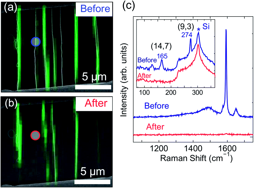 | ||
| Fig. 3 Superimposed Raman mapping and SEM images of SWNTs (a) before and (b) after the breakdown in a molecular glass film, respectively. Raman mapping images with an excitation wavelength of 532 nm show the integrated intensity of the G-band peaks ranging from 1500 to 1650 cm—1. (c) Raman spectra obtained from identical spots indicated in the SEM images. Inset: RBM spectrum of the SWNTs, which indicates the presence of a bundle of (9,3) and (14,7) SWNTs. | ||
Here, we discuss the mechanism of organic film-assisted electrical breakdown, which enables much longer SWNT length removal than that in air. The oxidation spread of SWNTs both in air and in organic films can be analogized to that of burning fuses for fireworks, along which the combustion reaction propagates from an ignition spot. Once the highest-temperature spot along an m-SWNT is broken, the Joule heating in the SWNT completely stops. How long the SWNT oxidation axially spreads is determined by the balance between heat generation from chemical reactions and heat dissipation to the environment after the SWNT breakdown occurs.
Whereas exothermic oxidation of SWNTs is the sole heat source for in-air breakdown, surrounding organic materials can be additionally oxidized and thereby generate heat in the case of organic film-assisted breakdown. Fig. 4(a–c) show SEM images of SWNT arrays before and after electrical breakdown in a molecular glass film and dissolution of the film with acetone, and an AFM image of the arrays after these processes. Fig. 4(d–f) show corresponding SEM and AFM images for electrical breakdown in a PMMA film, which also increased the removal length of SWNTs. From SEM observations, SWNTs were categorized into two parts after the breakdown process: the SWNTs which disappeared (removed parts) and the SWNTs which still remained on the substrates (unremoved parts). Comparison of the heights of the removed parts in the white dashed box of Fig. 4(c) and the unremoved parts along the same SWNTs after breakdown in the molecular glass film indicated that the removed parts were thicker (on average, ca. 2.2 nm) than the unremoved parts (on average, ca. 0.7 nm). This implies that molecular glass around the m-SWNTs was locally involved in chemical reactions with SWNTs and consequently became insoluble in acetone. The heat of oxidation from the surrounding organic materials, in addition to that from the SWNT, could induce axially-spread oxidation of the SWNT itself. In contrast, the thickness of the parts where breakdown occurred in the PMMA film was smaller (on average, ca. 0.75 nm) than that of the unremoved parts (on average, ca. 1.5 nm) [Fig. 4(f)]. This confirmed the long-length removal of SWNTs, although there was still a little amount of undissolved soot from the SWNTs or PMMA. The oxidation of PMMA could also induce long-length breakdown because the oxidation temperature of PMMA (ca. 304 °C) is lower than that of the SWNTs (500–700 °C (ref. 30)). A similar phenomenon was observed in the composite of cyclotrimethylene trinitramine (TNA) and multi-walled carbon nanotubes (MWNTs), where an exothermic chemical reaction of TNA initiated by laser irradiation propagates along MWNTs.31
 | ||
| Fig. 4 SEM images of an SWNT array (a) before and (b) after breakdown in a molecular glass film and dissolution of the film, and (c) the corresponding AFM image after these processes. (d–f) Equivalent images for breakdown in a PMMA film. White dashed boxes in the AFM images indicate the removed parts. | ||
Another effect of the organic film is to prevent the SWNTs from rapid cooling after breakdown, because the films are locally heated close to the SWNT temperatures by Joule heating of the SWNTs. This was supported by faster ramp-up voltage experiments on molecular glass films. When breakdown was performed with an increased ramp rate of drain voltage (ca. 4 V s−1) so that the film did not become sufficiently hot, the removal length (100–300 nm) was almost the same as that for in-air breakdown (data not shown). The function of the organic materials as heat reservoirs is explained by their lower thermal diffusivity (for example, PMMA; ca. 1.1 × 10⁻⁷ m2 s−1) than air (ca. 2.2 × 10⁻⁵ m2 s−1) at room temperature.
Contrary to the current study for full-length removal of SWNTs, previous attempts were reported to decrease the removal length by controlling heat generation and heat dissipation.32,33 Electrical breakdown in a reduced oxygen environment decreased the collision rate between oxygen molecules and SWNTs, resulting in a low heat generation rate from SWNT oxidation.32 By conducting electrical breakdown with short-distance electrodes, heat sinking to the metal electrodes has a large influence on the SWNT cooling rate.33,34
Uniform power dissipation along the SWNTs is also important for their full-length removal. When the SWNTs assigned as semiconducting by RBM spectra were purposely broken with negative gate voltages and high drain voltages, the removal lengths tended to be smaller (<1.5 μm) than those of m-SWNTs (data not shown). Asymmetric power dissipation along an s-SWNT due to a non-uniform electric field and charge density35,36 was thus the probable cause of shorter-length SWNT removal. Kinks in the SWNTs that originated from growth or transfer processes also generated non-uniform temperatures37 along the SWNT, and therefore resulted in partial breakdown (data not shown).
The maximum SWNT removal length and length consistency can be significantly improved by the appropriate selection of film materials in terms of their oxidation characteristics and thermal properties, or by reducing the non-uniformity of power dissipation caused by kinks in the SWNTs. The amount of oxygen molecules that permeate through the organic films is also an important factor for oxidation reaction of the films and SWNTs;32 therefore, the selection of film material and thickness should be considered. In order to completely eliminate m-SWNTs from certain areas, it is also necessary to grow all SWNTs with lengths long enough to connect a pair of electrodes, because electrically isolated m-SWNTs cannot be heated up. Under optimized conditions, organic film-assisted breakdown can yield arrays of pure s-SWNTs with larger areas, where a great number of FETs with high on/off ratios can be fabricated by simply placing electrodes without further purification processes. Further multiple fabrication of FETs using the s-SWNT arrays purified by organic film-assisted electrical breakdown is currently underway. Device fabrication based on s-SWNT arrays would enable SWNT-based large-scale integrated circuits or other semiconducting devices to be obtained.
4 Conclusions
In summary, a new technique was developed for the selective removal of long lengths of m-SWNTs using electrical breakdown in two types of organic films. High removal selectivity was supported by the transfer characteristics of FETs, and long-length removal of m-SWNTs in channel areas was confirmed by multiple analyses. A maximum removal length of 16.4 μm and spatial resolution of ca. 55 nm were attained, probably due to heat generation around the SWNTs by oxidation of the organic film and/or the heat accumulation effect of the organic materials.Acknowledgements
Part of this work was financially supported by Grants-in-Aid for Scientific Research (no. 22226006, 23760179, 25630063, 25107002), the IRENA Project of JST-EC DG RTD and the Strategic International Collaborative Research Program (SICORP). This work was partly conducted at the Center for Nano Lithography & Analysis, VLSI Design and Education Center (VDEC), and Laser Alliance, the University of Tokyo. K.O. was financially supported by the Iwadare Scholarship Foundation and Global Leader Program for Social Design and Management. T.I. was financially supported by the Japan Society for the Promotion of Science (JSPS) Fellowship (23-8717).Notes and references
- N. Patil, J. Deng, S. Mitra and H. S. P. Wong, IEEE Trans. Nanotechnol., 2009, 8, 37–45 CrossRef.
- M. M. Shulaker, G. Hills, N. Patil, H. Wei, H. Y. Chen, H. S. P. Wong and S. Mitra, Nature, 2013, 501, 526–530 CrossRef CAS PubMed.
- C. Kocabas, S. H. Hur, A. Gaur, M. A. Meitl, M. Shim and J. A. Rogers, Small, 2005, 1, 1110–1116 CrossRef CAS PubMed.
- H. Ago, K. Nakamura, K. Ikeda, N. Uehara, N. Ishigami and M. Tsuji, Chem. Phys. Lett., 2005, 408, 433–438 CrossRef CAS PubMed.
- J. Li, K. Liu, S. Liang, W. Zhou, M. Pierce, F. Wang, L. Peng and J. Liu, ACS Nano, 2014, 8, 554–562 CrossRef CAS PubMed.
- S. W. Hong, T. Banks and J. A. Rogers, Adv. Mater., 2010, 22, 1826–1830 CrossRef CAS PubMed.
- C. N. R. Rao, R. Voggu and A. Govindaraj, Nanoscale, 2009, 1, 96–105 RSC.
- Y. Li, D. Mann, M. Rolandi, W. Kim, A. Ural, S. Hung, A. Javey, J. Cao, D. Wang, E. Yenilmez, Q. Wang, J. F. Gibbons, Y. Nishi and H. Dai, Nano Lett., 2004, 4, 317–321 CrossRef CAS.
- G. Hong, B. Zhang, B. Peng, J. Zhang, W. M. Choi, J. Y. Choi, J. M. Kim and Z. Liu, J. Am. Chem. Soc., 2009, 131, 14642–14643 CrossRef CAS PubMed.
- W. Zhou, S. Zhan, L. Ding and J. Liu, J. Am. Chem. Soc., 2012, 134, 14019–14026 CrossRef CAS PubMed.
- X. Qin, F. Peng, F. Yang, X. He, H. Huang, D. Luo, J. Yang, S. Wang, H. Liu, L. Peng and Y. Li, Nano Lett., 2014, 14, 512–517 CrossRef CAS PubMed.
- A. D. Franklin, Nature, 2013, 498, 443–444 CrossRef CAS PubMed.
- M. S. Arnold, A. A Green, J. F. Hulvat, S. I. Stupp and M. C. Hersam, Nat. Nanotechnol., 2006, 1, 60–65 CrossRef CAS PubMed.
- H. Liu, D. Nishide, T. Tanaka and H. Kataura, Nat. Commun., 2011, 2, 309–316 CrossRef PubMed.
- Q. Cao, S. Han, G. S. Tulevski, Y. Zhu, D. D. Lu and W. Haensch, Nat. Nanotechnol., 2013, 8, 180–186 CrossRef CAS PubMed.
- M. Engel, J. P. Small, M. Steiner, M. Freitag, A. A. Green, M. C. Hersam and P. Avouris, ACS Nano, 2008, 2, 2445–2452 CrossRef CAS PubMed.
- B. K. Sarker, S. Shekhar and S. I. Khondaker, ACS Nano, 2011, 5, 6297–6305 CrossRef CAS PubMed.
- P. G. Collins, M. S. Arnold and P. Avouris, Science, 2001, 292, 706–709 CrossRef CAS PubMed.
- G. Zhang, P. Qi, X. Wang, Y. Lu, X. Li, R. Tu, S. Bangsaruntip, D. Mann, L. Zhang and H. Dai, Science, 2006, 314, 974–977 CrossRef CAS PubMed.
- G. Hong, M. Zhou, R. Zhang, S. Hou, W. Choi, Y. S. Woo, J. Y. Choi, Z. Liu and J. Zhang, Angew. Chem., Int. Ed., 2011, 50, 6819–6823 CrossRef CAS PubMed.
- S. Li, C. Liu, P. X. Hou, D. M. Sun and H. M. Cheng, ACS Nano, 2012, 6, 9657–9661 CrossRef CAS PubMed.
- S. H. Jin, S. N. Dunham, J. Song, X. Xie, J. H. Kim, C. Lu, A. Islam, F. Du, J. Kim, J. Felts, Y. Li, F. Xiong, M. A. Wahab, M. Menon, E. Cho, K. L. Grosse, D. J. Lee, H. U. Chung, E. Pop, M. A. Alam, W. P. King, Y. Huang and J. A. Rogers, Nat. Nanotechnol., 2013, 8, 347–355 CrossRef CAS PubMed.
- S. Maruyama, R. Kojima, Y. Miyauchi, S. Chiashi and M. Kohno, Chem. Phys. Lett., 2002, 360, 229–234 CrossRef CAS.
- S. Chiashi, H. Okabe, T. Inoue, J. Shiomi, T. Sato, S. Kono, M. Terasawa and S. Maruyama, J. Phys. Chem. C, 2012, 116, 6805–6808 CAS.
- T. Inoue, D. Hasegawa, S. Badar, S. Aikawa, S. Chiashi and S. Maruyama, J. Phys. Chem. C, 2013, 117, 11804–11810 CAS.
- L. Jiao, B. Fan, X. Xian, Z. Wu, J. Zhang and Z. Liu, J. Am. Chem. Soc., 2008, 130, 12612–12613 CrossRef CAS PubMed.
- P. T. Araujo, S. K. Doorn, S. Kilina, S. Tretiak, E. Einarsson, S. Maruyama, H. Chacham, M. A. Pimenta and A. Jorio, Phys. Rev. Lett., 2007, 98, 067401–067404 CrossRef.
- R. Y. Zhang, Y. Wei, L. A. Nagahara, I. Amlani and R. K. Tsui, Nanotechnology, 2006, 17, 272–276 CrossRef CAS.
- M. S. Dresselhaus, G. Dresselhaus, A. Jorio, A. G. S. Filho and R. Saito, Carbon, 2002, 40, 2043–2061 CrossRef CAS.
- Y. Murakami, Y. Miyauchi, S. Chiashi and S. Maruyama, Chem. Phys. Lett., 2003, 374, 53–58 CrossRef CAS.
- W. Choi, S. Hong, J. T. Abrahamson, J. H. Han, C. Song, N. Nair, S. Baik and M. S. Strano, Nat. Mater., 2010, 9, 423–429 CrossRef CAS PubMed.
- F. Xiong, A. D. Liao, D. Estrada and E. Pop, Science, 2011, 332, 568–570 CrossRef CAS PubMed.
- P. Qi, A. Javey, M. Rolandi, Q. Wang, E. Yenilmez and H. Dai, J. Am. Chem. Soc., 2004, 126, 11774–11775 CrossRef CAS PubMed.
- E. Pop, Nanotechnology, 2008, 19, 295202–295206 CrossRef PubMed.
- A. Liao, R. Alizadegan, Z. Y. Ong, S. Dutta, F. Xiong, K. J. Hsia and E. Pop, Phys. Rev. B: Condens. Matter Mater. Phys., 2010, 82, 205406–205409 CrossRef.
- C. L. Tsai, A. Liao, E. Pop and M. Shim, Appl. Phys. Lett., 2011, 99, 053120–053123 CrossRef PubMed.
- X. Xie, K. L. Grosse, J. Song, C. Lu, S. Dunham, F. Du, A. E. Islam, Y. Li, Y. Zhang, E. Pop, Y. Huang, W. P. King and J. A. Rogers, ACS Nano, 2012, 6, 10267–10275 CrossRef CAS PubMed.
| This journal is © The Royal Society of Chemistry 2014 |