 Open Access Article
 This Open Access Article is licensed under a
 Creative Commons Attribution 3.0 Unported Licence
SWNT nano-engineered networks strongly increase charge transport in P3HT
Nicolas
Boulanger
,
Junchun
Yu
and
David R.
Barbero
*
Umeå Universitet, Institutionen för Fysik, Linnaeus väg 24, Umeå, Sweden. E-mail: david.barbero@physics.umu.se
First published on 8th May 2014
Abstract
We demonstrate the formation of arrays of 3D nanosized networks of interconnected single-wall carbon nanotubes (SWNTs) with well defined dimensions in a poly-3-hexylthiophene (P3HT) thin film. These novel nanotube nano-networks produce efficient ohmic charge transport, even at very low nanotube loadings and low voltages. An increase in conductivity between one and two orders of magnitude is observed compared to a random network. The formation of these nano-engineered networks is compatible with large area imprinting and roll to roll processes, which makes it highly desirable for opto-electronic and energy conversion applications using carbon nanotubes.
Carbon nanotubes and polymer composites have recently emerged as a new class of materials with enhanced electrical and/or mechanical properties. In particular, due to their exceptional charge transport, single walled carbon nanotubes are becoming increasingly attractive as additives in semi-conducting polymers, such as the widely used P3HT, for next generation of hybrid and organic photovoltaic devices.1–6 Recent advances in this field have shown that ultrafast charge transport readily occurs at the interface between SWNTs and P3HT.7–9 The nanotubes act as highly efficient charge transport pathways, between the P3HT interface and an electrode. However, one important condition for efficient and optimal charge transport is the ability to form a continuous (percolated) network of interconnected tubes between the two interfaces. This aspect has often been overlooked, and several studies have shown that current methods used to form nanotube networks for electronic applications result in random networks with non-optimal charge transport.10 The methods typically used to form random networks are spin-coating or drop casting from solution, and they result in non-controlled tube interconnection and in nanotube positioning which is random and not necessarily reproducible (see Fig. 1A). Controlled dispersion of the nanotubes and formation of a continuous (percolated) network of interconnected tubes inside a polymer matrix are important for better charge transport and reproducible electrical properties. We have recently demonstrated a new method which enables the formation of continuous SWNT networks in well ordered nanoscale domains, as shown in Fig. 1B and 1C.11 The high degree of control provided by this method results in nano-engineered networks with much increased charge transport. In this communication, we demonstrate that such nano-engineered networks strongly enhance charge transport in a P3HT matrix compared to a random network produced by spin-coating over a wide range of nanotube loadings. By varying the concentration of tubes, we show that efficient charge transport occurs at all concentrations, even at very low nanotube loading, much below the percolation threshold (ϕc) typically reported for P3HT. Moreover, we find that the charge transport mechanism is very different in the two types of networks, with the nano-networks producing ohmic conduction and high conductivity at all concentrations and even at low voltages. A high nanotube loading has often been seen as the most important parameter for efficient charge transport and to obtain high conductivity in nanotube composites. We instead show that the nanoscale interconnectivity of the nanotubes inside the composite is the main factor which influences charge transport, and that high loadings in random networks still produce less efficient conducting pathways compared to nano-engineered networks with much lower concentrations of tubes. Solution processed methods such as spin-coating or drop-casting require much higher concentrations of nanotubes in order to render the composite conductive. This increases material costs, but it also increases the probability to create bundles which have been shown to decrease charge transport and lower the device performance.12,13
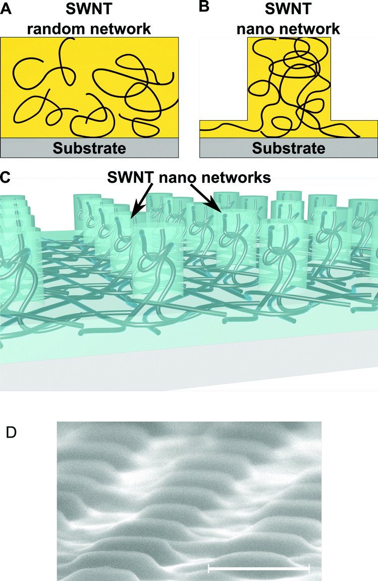 | ||
| Fig. 1 Network configuration in (a) a random network and (b) a nano-engineered network. The interconnection between nanotubes and the ability to form a continuous path for efficient charge transport is higher in the nano-engineered network. Figure (c) represents a 3D view of an array of nanotube nano-networks and (d) is a scanning electron micrograph of the nano-networks embedded in P3HT. The scale bar is 400 nm. | ||
By increasing the nanoscale interconnectivity of the tubes inside the nano-network, we were able to strongly reduce the concentration required (much below the percolation threshold previously reported) for forming efficient charge transport pathways. Charge transport in P3HT was strongly enhanced at all concentrations compared to a random network produced by traditional solution based methods. The low amount of SWNTs used reduces bundling and provides an economical solution for electronic applications because much lower amounts of expensive nanotubes are necessary. The nanotubes used were mostly semi-conducting (>90%) and were used as purchased from the manufacturer (SouthWest NanoTechnologies) without any purification or doping. The nanotubes were dispersed in ortho-dichlorobenzene (o-DCB), and ultrasonicated for 60 minutes. The SWNT nano-networks were produced by spin-coating a thin layer of nanotubes and an additional layer of regio-regular P3HT (Mw = 24![[thin space (1/6-em)]](https://www.rsc.org/images/entities/char_2009.gif) 000 g mol−1) onto a doped conductive silicon substrate (resistivity 0.002–0.005 Ω cm). This configuration was then nanoimprinted with a soft mold made of polydimethylsiloxane (PDMS) with 400 nm wide and 350 nm high pillars at 200 °C and 20 bar.14 The random networks were produced by spin-coating a thin-film from a solution of P3HT and nanotubes mixed together. Films with different nanotube concentrations ranging from ≈100 times below the reported percolation threshold (ϕc ≈ 2–3 wt%) in P3HT to 3 wt% were produced by the methods described above.15Fig. 1 shows the nanoscale network organization in (a) a typical random network and (b) a nano-patterned network inside a thin film. In the random network, the tubes are not optimally interconnected and only a small portion contributes to charge transport across the film thickness. By contrast, the formation of nano-patterned networks results in much more efficient percolation between tubes and results in a strong increase in electrical conduction, even at low loadings. The concentrations of SWNTs used range from ≈0.03 wt% to ≈3 wt%, and the details of the samples prepared and measured here are indicated in Table 1.
000 g mol−1) onto a doped conductive silicon substrate (resistivity 0.002–0.005 Ω cm). This configuration was then nanoimprinted with a soft mold made of polydimethylsiloxane (PDMS) with 400 nm wide and 350 nm high pillars at 200 °C and 20 bar.14 The random networks were produced by spin-coating a thin-film from a solution of P3HT and nanotubes mixed together. Films with different nanotube concentrations ranging from ≈100 times below the reported percolation threshold (ϕc ≈ 2–3 wt%) in P3HT to 3 wt% were produced by the methods described above.15Fig. 1 shows the nanoscale network organization in (a) a typical random network and (b) a nano-patterned network inside a thin film. In the random network, the tubes are not optimally interconnected and only a small portion contributes to charge transport across the film thickness. By contrast, the formation of nano-patterned networks results in much more efficient percolation between tubes and results in a strong increase in electrical conduction, even at low loadings. The concentrations of SWNTs used range from ≈0.03 wt% to ≈3 wt%, and the details of the samples prepared and measured here are indicated in Table 1.
| SWNT conc. (wt%) | Nano-network | Random network |
|---|---|---|
| 0.03 | 1.11 | 1.37 |
| 0.12 | 1.02 | 1.66 |
| 0.48 | 1.05 | 1.64 |
| 1.50 | 1.11 | 1.90 |
| 3.00 | 1.09 | 1.33 |
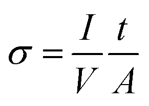
Fig. 2 shows the conductivity of the SWNT/P3HT composite films with either a random network or a nano-engineered network of nanotubes as a function of the voltage applied between the top and the bottom of the film. The voltage was varied with a small step of 0.1 V, and the current flowing across the film (from top to bottom) was measured for each applied voltage. In the case of the nanopatterns, the current was measured between the top and the bottom of the pattern. Measurements were repeated up to 10 times in each location, and in 3 different locations on each sample, and showed good reproducibility. The conductivity σ was calculated for each applied voltage as
 | (1) |
This indicates more efficient charge transport and much better interconnectivity between tubes in the nano-networks at low concentrations. Fig. 3A shows the increase in conductivity (in number of times increased) of (σnano − σrandom) divided by σrandom as a function of the concentration of nanotubes at 0.3 V applied voltage. At all concentrations below 3.0 wt%, the random network did not form an efficient network for charge transport, which is consistent with previously published results. However, the nano-network is already 5 times more conductive at the lowest concentration of 0.03 wt%, and becomes more and more conductive with higher loadings, reaching a peak of ≈100 times more conductive than the random network at a concentration of ≈1.5 wt%. Close to the percolation threshold of the random network (≈3.0 wt%), σrandom increases as expected but the nano-network still remains nearly 20 times more conductive. Moreover, it can be noticed in Fig. 2 that the conductivity in the nano-network is also nearly constant from low to high applied voltage, whereas the conductivity in the random network is much lower at low voltage, and it increases at higher voltage. This shows that nano-engineering of the tube network however provides much better charge transport at low voltage (≈0.2–1.0 V), which is advantageous for certain applications, e.g. organic and hybrid photovoltaics.16
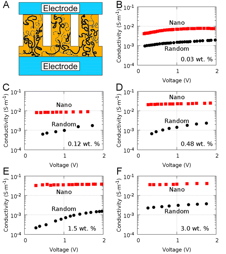 | ||
| Fig. 2 Schematics of the conductivity measurements in the nano-networks (a). Conductivity of random networks and nano-networks of SWNTs in a P3HT film at various nanotube concentrations: (b) 0.03 wt%, (c) 0.12 wt%, (d) 0.48 wt%, (e) 1.50 wt%, and (f) 3.00 wt%. | ||
 | ||
| Fig. 3 Electrical characteristics of the networks. (a) Increase in conductivity in the nano-network compared to the random network as a function of nanotube concentrations at low voltage (0.3 V). (b) Typical current density–voltage characteristics of random and nano-networks, showing ohmic conduction in the nano-network (a ≈ 1.0) and non-ohmic conduction in the random network. | ||
The current density (J)–voltage (V) characteristics for the random and the nano networks are shown in Fig. 3B. The data were fitted with a power law: J = bVa where J is the measured current density and V is the applied voltage. In a log–log plot, as shown in Fig. 3, the exponent a gives the slope of the relationship between J and V and is reported in Table 1 at all concentrations.17 Very different behavior is observed between the typical random network and the nano-engineered network. The nano-networks display an exponent a ≈ 1.02–1.11 at all concentrations, which is characteristic of ohmic conduction. By contrast, conduction in the random network is clearly non-ohmic, with values of the exponent a ≈ 1.33–1.90. Conduction in pure P3HT has been described as space-charge limited with a quadratic variation of the current density with voltage (a = 2). The values of a measured in the random network indicate a conduction which is partially space-charge limited, and which is likely due to poor interconnection between tubes inside the film which leads to non-ohmic charge transport, and much lower conductivities compared to the nano-network. Ohmic conduction in the nano-scale networks can be explained by the formation of continuous paths with highly interconnected tubes which bridge the gap between the top and the bottom of the film. During the formation of nano-networks, the nanotubes are pushed into the cavities of the patterned mold by shear forces acting on the SWNT/polymer composite. The nanotubes were first oriented in the plane of the film, in a quasi-2D geometry (film's thickness ≈ 20 nm). When the second layer of pure P3HT is spun on top of the nanotubes, the film's conductivity remains identical to that of pure P3HT (σ ≈ 10−3 S m−1). After formation of the nano-networks in this composite film, the conductivity increases by more than one order of magnitude to σ ≈ 10−2 S m−1 at a low SWNT concentration of ≈0.03 wt%.
This 10 fold increase in conductivity in the nano-networks clearly shows that the nanotubes are reoriented from a planar orientation to a more vertical orientation during nano-network formation. This re-orientation of the tubes can be explained by the flow of the composite inside the mold which fills the cavity from the bottom to its top as shown in Fig. 4.18–21 The nanotubes are therefore dragged with the flow of the liquid composite and form a conducting path from top to bottom of the patterns. Considering the pattern dimensions (≈400 nm diameter and ≈300 nm high), it is even possible that single nanotubes form a direct conducting path by bridging the whole film thickness. Indeed, the average length of the nanotube is ≈700 nm, which is longer than the thickness of the nanopatterned film (≈400 nm). The film thickness in the random network is ≈120 nm, and tube bridging would be expected here too, but it is clearly not observed from the low conductivity measured in the random networks. This shows that efficient pathways and contacts are formed from top to bottom of the film during flow of the tubes inside the nano-network, which leads to a different architecture with a higher degree of interconnection between tubes compared to a typical random network formed by spin-coating.
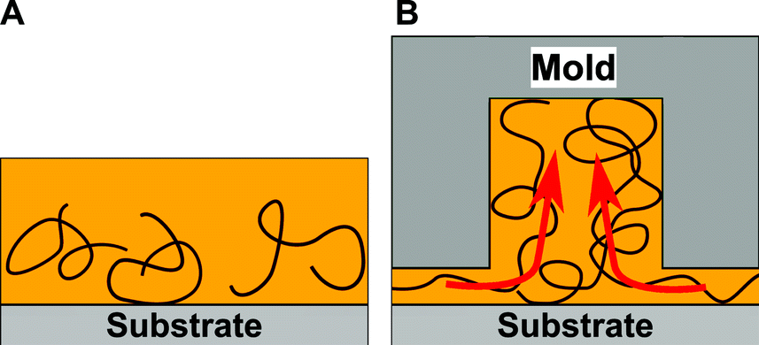 | ||
| Fig. 4 Mechanism of nano-network formation. Figure (a) represents a two-layer composite film with nanotubes and a polymer film. Figure (b) shows formation of the nano-network, where the arrows indicate flow of nanotubes inside the mold's cavity to form a pathway for charge transport from the top to the bottom of the pattern. | ||
In conclusion, we have shown that the formation of an array of well-defined nano-scale networks of nanotubes produces efficient charge transport inside a P3HT film, with an increase in conductivity by as much as ≈100 times compared to a traditional random network. The nano-networks showed ohmic conduction at all concentrations, and a nearly constant conductivity at all applied voltages, including low voltages (<0.5 V). We believe these novel nano-engineered networks should be very appealing for hybrid and carbon based energy conversion devices such as photovoltaic solar cells.
Acknowledgements
The authors thank the Baltic Foundation for financial support. D. R. B. is also thankful for a Young Researcher Career Award from Umeå University for supporting this work.References
- M. W. Rowell, M. A. Topinka, M. D. McGehee, H.-J. Prall, G. Dennler, N. S. Sariciftci, L. Hu and G. Gruner, Appl. Phys. Lett., 2006, 88, 233506 CrossRef PubMed.
- F. S. Kim, G. Ren and S. A. Jenekhe, Chem. Mater., 2011, 23, 682–732 CrossRef CAS.
- E. Kymakis, M. M. Stylianakis, G. D. Spyropoulos, E. Stratakis, E. Koudoumas and C. Fotakis, Sol. Energy Mater. Sol. Cells, 2012, 96, 298–301 CrossRef CAS PubMed.
- C. Niu, MRS Bull., 2011, 36, 766–773 CrossRef CAS.
- Z. Yang, T. Chen, R. He, G. Guan, H. Li, L. Qiu and H. Peng, Adv. Mater., 2011, 23, 5436–5439 CrossRef CAS PubMed.
- H. Derbal-Habak, C. Bergeret, J. Cousseau and J. M. Nunzi, Sol. Energy Mater. Sol. Cells, 2011, 95, S53–S56 CrossRef CAS PubMed.
- D. J. Bindl, N. S. Safron and M. S. Arnold, ACS Nano, 2010, 4, 5657–5664 CrossRef CAS PubMed.
- M. Bernardi, M. Giulianini and J. Grossman, ACS Nano, 2010, 4, 6599–6606 CrossRef CAS PubMed.
- S. D. Stranks, C. Weisspfennig, P. Parkinson, M. B. Johnston, L. M. Herz and R. J. Nicholas, Nano Lett., 2011, 11, 66–72 CrossRef CAS PubMed.
- J. Di, Z. Yong, X. Zheng, B. Sun and Q. Li, Small, 2013, 9, 1367–1372 CrossRef CAS PubMed.
- D. R. Barbero, N. Boulanger, M. Ramstedt and J. Yu, Adv. Mater., 2014, 26, 3111–3117 CrossRef CAS PubMed.
- J. Yang, N. Yang, D. Zhang, X. Wang, Y. Li and Y. Li, J. Phys. Chem. C, 2012, 116, 22028–22035 CAS.
- P. Luo, H. Wu and M. Morbidelli, Carbon, 2014, 68, 610–618 CrossRef CAS PubMed.
- D. R. Barbero, M. S. M. Saifullah, P. Hoffmann, H. J. Mathieu, D. Anderson, G. A. C. Jones, M. E. Welland and U. Steiner, Adv. Funct. Mater., 2007, 17, 2419–2425 CrossRef CAS.
- I. Singh, P. Bhatnagar, P. Mathur, I. Kaur, L. Bharadwaj and R. Pandey, Carbon, 2008, 46, 1141–1144 CrossRef CAS PubMed.
- S. A. Gevorgyan, O. Zubillaga, J. M. V. de Seoane, M. Machado, E. A. Parlak, N. Tore, E. Voroshazi, T. Aernouts, H. Mllejans, G. Bardizza, N. Taylor, W. Verhees, J. M. Kroon, P. Morvillo, C. Minarini, F. Roca, F. A. Castro, S. Cros, B. Lechne, J. F. Trigo, C. Guilln, J. Herrero, B. Zimmermann, S. B. Sapkota, C. Veit, U. Wrfel, P. S. Tuladhar, J. R. Durrant, S. Winter, S. Rousu, M. Vlimki, V. Hinrichs, S. R. Cowan, D. C. Olson, P. Sommer-Larsen and F. C. Krebs, Renewable Energy, 2014, 63, 376–387 CrossRef CAS PubMed.
- Z. Chiguvare, J. Parisi and V. Dyakonov, J. Appl. Phys., 2003, 94, 2440–2448 CrossRef CAS PubMed.
- L. J. Heyderman, H. Schift, C. David, J. Gobrecht and T. Schweizer, Microelectron. Eng., 2000, 54, 229–245 CrossRef CAS.
- Y. Xu, F. Tsumori, T. Toyooka, H. Kotera and H. Miura, Jpn. J. Appl. Phys., 2011, 50, 06GK11 CrossRef.
- D. Jun, W. Zhengying, L. Shize and T. Yiping, Microsyst. Technol., 2013, 19, 1229–1238 CrossRef PubMed.
- L. Peng, Y. Deng, P. Yi and X. Lai, J. Micromech. Microeng., 2014, 24, 013001 CrossRef.
| This journal is © The Royal Society of Chemistry 2014 |