 Open Access Article
 This Open Access Article is licensed under a Creative Commons Attribution-Non Commercial 3.0 Unported Licence
Electrochemical construction of hierarchically ordered CdSe-sensitized TiO2 nanotube arrays: towards versatile photoelectrochemical water splitting and photoredox applications†
Fang-Xing
Xiao
,
Jianwei
Miao
,
Hsin-Yi
Wang
,
Hongbin
Yang
,
Jiazang
Chen
and
Bin
Liu
*
School of Chemical and Biomedical Engineering, Nanyang Technological University, 62 Nanyang Drive, Singapore 637459, Singapore. E-mail: liubin@ntu.edu.sg; Fax: +65 6794-7553; Tel: +65 6513-7971
First published on 21st April 2014
Abstract
Recent years have witnessed quite a number of worldwide efforts for fabricating CdSe/TiO2 nanotube arrays (CdSe/TNTAs) nanocomposites; however, the construction of a well-defined CdSe/TNTAs binary nanostructure for versatile photocatalytic and photoelectrochemical applications still poses a big challenge. In this work, a hierarchically ordered CdSe/nanoporous TiO2 nanotube arrays (CdSe/NP-TNTAs) hybrid nanostructure was fabricated through a facile electrochemical deposition strategy. The combined structural and morphological characterizations show that the CdSe ingredients, consisting of clusters of quantum dots, were uniformly assembled on the inner and outer surfaces of the NP-TNTAs framework. It was demonstrated that the CdSe/NP-TNTAs heterostructure could be utilized as an efficient photoanode for photoelectrochemical water splitting; moreover, it could be used as a multifunctional photocatalyst for photoredox applications, including the photocatalytic oxidation of organic dye pollutants and the selective reduction of aromatic nitro compounds under visible light irradiation. Furthermore, photoelectrochemical and photocatalytic mechanisms over the CdSe/NP-TNTAs heterostructure were elucidated. In addition, the predominant active species during the photocatalytic process were systematically explored and unequivocally determined. It is hoped that this work could promote further interest in the fabrication of various one dimensional NP-TNTAs-based composite materials and their applications to photoelectrochemical water splitting and photocatalytic selective redox applications.
1. Introduction
In recent years, heterogeneous photocatalysis by semiconductor nanomaterials has received enormous research attention and achieved extensive applications in diverse fields, including environment remediation, selective organic transformation to fine chemicals, clean H2 production, and antibacterial activity.1,2 Titanium dioxide (TiO2) as a quintessential semiconductor has been extensively studied for photocatalysis due to its inherent merits of nontoxicity, physical and chemical stability, and peculiar electronic and optical properties.3 More recently, one-dimensional (1-D) TiO2 nanostructures (e.g. nanowires, nanorods, nanobelts, and nanotubes) have shown intrinsic capabilities of independently modulating carrier diffusion length and light absorption depth.4–7 In particular, highly ordered, vertically oriented TiO2 nanotube arrays (TNTAs) prepared by the anodization of Ti foils has been emerging as a promising candidate for photoelectrochemical and photocatalytic applications on account of their aligned porosity, large internal specific surface area, oriented tubular structure, and suitable electrical properties, which are advantageous for the vectorial collection of charge carriers by building an attractive electron percolation pathway along the long axis of nanotubes when compared with its conventional particulate counterparts.8Although considerable research efforts have been devoted for fabricating a diverse range of TNTAs-based electrodes and photocatalysts, their performances are far from satisfactory. The predominant reason is the large bandgap energy of TiO2 (viz. 3.2 eV for anatase and 3.0 eV for rutile) that limits its optical absorption within only the UV light region.9 Therefore, to overcome this obstacle, various strategies have been developed to tune the photoresponse of 1-D TiO2 nanostructures to visible light, such as the deposition of metal nanoparticles (e.g. Au, Ag, Pt),10,11 doping with transition metallic or non-metallic elements (e.g. N, C, S, I, F),12–16 and combination with secondary semiconductors (e.g. CdS, CdSe, CdTe, PbS, Bi2O3, InP).17–25 Among which, 1-D TiO2 nanostructures (e.g. TNTAs) decorated with narrow bandgap semiconductors have been demonstrated to be convenient systems for light harvesting by virtue of enhanced visible light absorption, efficient charge carrier injection and transport in the ordered nanostructure.26
CdSe, as one of the most important II–VI semiconductors, has been widely utilized to modify TiO2 for photoelectrochemical or photocatalytic applications.26–29 Notwithstanding these advances in the fabrication of CdSe/TiO2 nanocomposites, the rational design and controllable synthesis of hierarchically ordered 1-D CdSe/TNTAs heterostructures with versatile photoelectrochemical and photocatalytic performances still remain as a significant challenge. It is noteworthy that CdSe/TNTAs nanocomposites exhibit inimitable advantage over their conventional particulate counterparts. Firstly, the regular pore structure and relatively large pore size of TNTAs allow for the uniform distribution of CdSe on the whole framework. Secondly, highly ordered perpendicularly aligned TNTAs permit direct charge transfer along the length of the nanotube arrays to the conductive substrate (i.e. Ti foil), which remarkably reduces the loss incurred by charge-hopping across the grain boundaries of bulk nanoparticles. Currently, synthetic strategies toward CdSe/TNTAs nanocomposites are primarily confined to the following methods, namely, static soaking using bi-functional linker molecules30,31 photoassisted electrodeposition,32 chemical bath deposition,33 and spray pyrolysis deposition.34 Despite these endeavors, it should be emphasized that these synthetic protocols are inevitably complicated and time-consuming to some extent. More importantly, in most cases, the monodisperse deposition of CdSe ingredients on TNTAs in conjunction with intimate interfacial interaction is far from satisfactory. On the contrary, the electrochemical deposition technique has been demonstrated to be a straightforward and pragmatic method for the large-scale fabrication of nanomaterials due to its intrinsic simplicity, template-free design, low cost, and environmental friendliness.35,36
Herein, a hierarchically ordered nanoporous-layer-covered TNTAs (NP-TNTAs) scaffold was uniformly decorated with CdSe via a facile electrochemical deposition approach that yields well-defined CdSe/NP-TNTAs nanocomposites. It was demonstrated that the as-constructed CdSe/NP-TNTAs heterostructure could be utilized as an efficient photoanode for photoelectrochemical water splitting and a multifunctional visible-light-driven photocatalyst for photocatalytic redox reactions, including the photodegradation of organic dye pollutants and photocatalytic hydrogenation of aromatic nitro compounds under ambient conditions. Moreover, the predominant active species accounting for the significantly enhanced photoredox performances of CdSe/NP-TNTAs heterostructures were undoubtedly determined. Furthermore, the photocatalytic and photoelectrochemical mechanisms of the CdSe/NP-TNTAs hybrid nanostructure were tentatively presented. It is anticipated that our current work could provide new insights for the fabrication of hierarchical narrow bandgap semiconductor/1-D semiconductor nanocomposites for versatile photocatalytic and photoelectrochemical applications.
2. Experimental section
2.1 Materials
Titanium sheets (50 mm × 20 mm × 0.1 mm, 99.9%), deionized water (DI H2O, Millipore, 18.2 MΩ cm resistivity), graphite sheet (50 mm × 20 mm × 0.1 mm, 99.6%), ethylene glycol ((CH2OH)2), ammonium fluoride (NH4F), hydrogen fluoride (HF), and element Se. N,N-Dimethylformamide (DMF), cadmium chloride (CdCl2·2.5H2O), sodium sulfide (Na2S·9H2O), sodium hydroxide (NaOH), ammonium formate (HCO2NH4), potassium thiosulfate (K2S2O8), 4-nitroaniline (4-NA), 2-nitroaniline (2-NA), and 3-nitroaniline (3-NA). All chemical reagents were of analytical grade and used as received without further purification.2.2 Preparation of NP-TNTAs
Ti foil was thoroughly cleaned by sonication in acetone, ethanol and DI H2O. Then, Ti sheets were immersed in a mixed solution of HF–HNO3–H2O in a volume ratio of 1![[thin space (1/6-em)]](https://www.rsc.org/images/entities/char_2009.gif) :4:5 for 30 s, washed by DI H2O and dried with a N2 stream. Anodization was carried out under ambient conditions at 50 V for 2 h with ca. 3 cm separation distance between the working (Ti foil) and counter electrode (graphite). The electrolyte consisted of 0.3 wt% of NH4F in ethylene glycol (196 mL) and DI H2O (4 mL). After anodization, the as-obtained TiO2 nanotube arrays were completely washed by DI H2O and dried with a N2 stream. Then, the nanotubes were removed from the Ti foil by sonication in ethanol for 5 min. A second anodization was subsequently performed at 50 V for 30 minutes to produce the hierarchically ordered NP-TNTAs. Similarly, the resulting NP-TNTAs were also washed by DI H2O, dried using a N2 stream and finally calcined at 450 °C for 1 h in air with a heating rate of 2 °C min−1.
:4:5 for 30 s, washed by DI H2O and dried with a N2 stream. Anodization was carried out under ambient conditions at 50 V for 2 h with ca. 3 cm separation distance between the working (Ti foil) and counter electrode (graphite). The electrolyte consisted of 0.3 wt% of NH4F in ethylene glycol (196 mL) and DI H2O (4 mL). After anodization, the as-obtained TiO2 nanotube arrays were completely washed by DI H2O and dried with a N2 stream. Then, the nanotubes were removed from the Ti foil by sonication in ethanol for 5 min. A second anodization was subsequently performed at 50 V for 30 minutes to produce the hierarchically ordered NP-TNTAs. Similarly, the resulting NP-TNTAs were also washed by DI H2O, dried using a N2 stream and finally calcined at 450 °C for 1 h in air with a heating rate of 2 °C min−1.
2.3 Preparation of CdSe/NP-TNTAs heterostructure
CdSe QDs were electrochemically deposited on the NP-TNTAs substrate from a mixed aqueous solution composed of 10 mM CdCl2 and 5 mM element Se in 30 mL of DMF. The electrochemical deposition was performed at 130 °C using a two-electrode set-up, in which blank Ti foils or NP-TNTAs were used as the working electrode and Pt plate, the counter electrode. During deposition, a constant current density of −0.55 mA cm−2 was applied to the NP-TNTAs working electrode. For comparison, a CdSe/TiO2 particulate film and a pure CdSe film were also prepared on a Ti foil through the same electrochemical deposition approach. The synthetic protocols for the preparation of the CdSe/TiO2 particulate film and pure CdSe film are analogous to that of the CdSe/NP-TNTAs heterostructure, except that the NP-TNTAs substrate was replaced with a TiO2 particulate film or blank Ti foil. The TiO2 particulate film was prepared by sonication-assisted protocol; in particular, TNTAs obtained from the conversational one-step anodization were continuously ultrasonicated for 120 min and subsequently subjected to calcination (450 °C, 3 h, in air), thus giving rise to a TiO2 particulate film grown directly on the Ti foil.2.4 Characterization
The phase composition was determined by X-ray diffraction (XRD) using a Bruker D8 Advance X-ray diffractometer with Cu Kα radiation. The accelerating voltage and applied current were 40 kV and 40 mA, respectively. Transmission electron microscopy (TEM) and high-resolution transmission electron microscopy (HRTEM) images were obtained by a JEOL model JEM 2010 EX instrument at an accelerating voltage of 200 kV. UV-vis diffuse reflectance spectra (DRS) were recorded on a Varian Cary 500 Scan UV-vis-NIR spectrometer, in which BaSO4 was used as the background from 200 nm to 800 nm. X-ray photoelectron spectroscopy (XPS) measurements were conducted on an ESCALAB 250 photoelectron spectrometer (Thermo Fisher Scientific) at 2.4 × 10⁻¹⁰ mbar using a monochromatic Al Kα X-ray beam (1486.60 eV). The binding energy (BE) of the element was calibrated to the BE of carbon (284.60 eV). The morphologies of the samples were measured by field-emission scanning electron microscopy (FESEM, JEOL JSM6701F).2.5 Photoelectrochemical measurements
Photoelectrochemical measurements were carried out on a CHI electrochemical analyzer (CHI 660B) using a standard three-electrode mode with 1 M NaOH (pH = 13.9) solution as the electrolyte. The NP-TNTAs or CdSe/NP-TNTAs were used as the working electrode, a Pt sheet (1 cm × 2 cm) served as the counter-electrode, and Ag/AgCl (KCl) electrode as the reference electrode. A 150 W Xe lamp (LEICA 150X) equipped with a band-pass light filter (λ > 420 nm) was applied as the light source.2.6 IPCE measurement
The incident photon-to-current conversion efficiency (IPCE) was measured under zero-bias (two-electrode, short-circuit) condition. The monochromatic light was supplied by Xe lamp irradiation through a monochromator (Newport). A chopper was placed in front of the monochromator, and the signal was collected using a lock-in radiometry (Merlin) after amplification by the current preamplifier.2.7 Photocatalytic activity
| Conversion (%) = [(C0 − C)/C0] × 100 |
3. Results and discussion
The flowchart depicting the electrochemical construction of hierarchically ordered CdSe/NP-TNTAs heterostructure via two-step anodization strategy followed by electrochemical deposition is displayed in Scheme 1. Note that the TNTAs substrate fabricated by the conventional one-step anodization approach always suffers from disparity in tube length and exhibits a rough top surface with very poor alignment (Fig. S1†). In contrast, the two-step anodization strategy, consisting of the first anodization for the growth of TNTAs and subsequent removal through sonication and the second anodization to grow NP-TNTAs from the same substrate, offers a convenient way for the preparation of much more uniform and well-aligned TiO2 nanotube arrays.41 Furthermore, it has been well established that NP-TNTAs, consisting of a periodically porous top layer and vertically aligned bottom tubular arrays, exhibit remarkably less structural defects in comparison with TNTAs.42–46 In addition, it has been reported that the top-layer of NP-TNTAs can serve as photonic crystals to enhance the optical absorption of NP-TNTAs.47 In this regard, in our work, the NP-TNTAs framework was selected as the substrate for the fabrication of the CdSe/NP-TNTAs heterostructure. | ||
| Scheme 1 Schematic illustration describing the fabrication of hierarchically ordered CdSe/NP-TNTAs heterostructure. | ||
3.1 Synthesis and characterization of CdSe/NP-TNTAs heterostructure
CdSe nanocrystals were precipitated on the NP-TNTAs framework through the following redox reaction: Cd2+ + Se + 2e− → CdSe.48,49 The morphologies of the CdSe/NP-TNTAs heterostructure were examined by field-emission scanning electron microscopy (FESEM). Fig. 1a and b show the top view FESEM images of NP-TNTAs scaffold attained by two-step anodization, which exhibits a regular pore structure with uniform size distribution of around 80 nm. Cross-sectional FESEM images (Fig. S2† and 1c) reveal that the NP-TNTAs film with a thickness of around 9 μm is composed of a highly periodic porous top layer and vertically aligned bottom tubular arrays growing vertically from the Ti substrate with a rather smooth surface. This implies that the well-ordered pore structure and the smooth surface of NP-TNTAs are well preserved after the heat treatment (450 °C, 1 h, in air), indicating that the calcination treatment did not alter the morphology of NP-TNTAs. As shown in Fig. 1d–f and S3,† when CdSe was electrochemically deposited on the NP-TNTAs scaffold, both the interior and exterior surfaces of NP-TNTAs were homogeneously coated with CdSe without any obvious particle agglomerations, suggesting the electrochemical deposition strategy developed in our work is rather efficient to achieve the CdSe functionalization on 1-D TiO2 nanotubes.49 The FESEM images of CdSe/NP-TNTAs heterostructure prepared by varying the deposition time are illustrated in Fig. S4,† all of which reveal an analogous morphology; nevertheless, it is worth mentioning that if the deposition time was too long (>2000 s), large agglomerations of CdSe nanoparticles appear, which seriously blocks the pores of NP-TNTAs. Fig. S5† shows the close observation to the morphology of a pure CdSe film deposited on a Ti foil via the same electrochemical deposition technique that reveals the fact that a CdSe film is virtually composed of various densely packed nanoparticles with a diameter of around 10 nm, which is in reasonable agreement with our previous result.49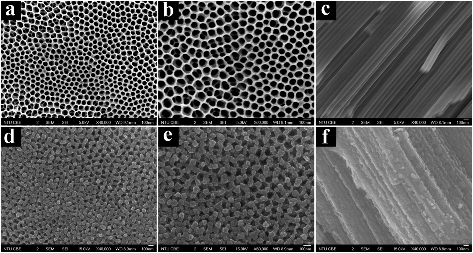 | ||
| Fig. 1 FESEM images of (a–c) NP-TNTAs and (d–f) CdSe/NP-TNTAs heterostructure prepared via electrochemical deposition with deposition time of 1600 s. | ||
Fig. 2 shows the XRD patterns of the NP-TNTAs substrate before and after calcination and the CdSe/NP-TNTAs heterostructure. The peaks (Fig. 2a and b) at 2θ values of 25.3°, 37.8°, 48.0°, 53.9°, 62.7°, and 75.0° are indexed to the (101), (004), (200), (105), (204), and (215) crystal planes of anatase TiO2 (JCPDS no. 21-1272), respectively, which indicates that calcination (i.e. 450 °C, 1 h, in air) is beneficial for the transformation of NP-TNTAs from the amorphous to anatase phase. The peaks at 2θ values of 24.0°, 25.3°, 27.5°, and 41.6° in Fig. 2c could be attributed to the (100), (002), (101), and (220) crystallographic planes of wurtzite CdSe (JCPDS no. 72-2307), respectively. Note that the diffraction peak of (002) for the CdSe phase was shielded by the peak arising from the (101) crystal plane of anatase TiO2.
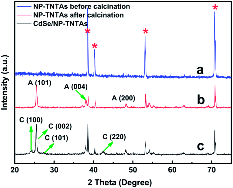 | ||
| Fig. 2 XRD patterns of NP-TNTAs (a) before and (b) after calcination (450 °C, 1 h, in air), and (c) CdSe/NP-TNTAs heterostructure. C: CdSe, A: Anatase, the asterisks denotes Ti patterns from Ti foil. | ||
UV-vis diffuse reflectance spectra (DRS) were utilized to determine the optical properties of the samples. It can be clearly seen from Fig. 3a that both NP-TNTAs and CdSe/NP-TNTAs heterostructure exhibit a pronounced adsorption band in the region spanning from 300 to 400 nm, which is ascribed to the electron excitation from the valence band to the conduction band of TiO2.50 It should be particularly pointed out that the absorption band of NP-TNTAs within the range of 500–800 nm stems from its unique hierarchically ordered nanostructure and excellent morphology uniformity, as shown in Fig. 1a–c, which is in accordance with a previous report.41 For comparison, the DRS results of TNTAs and TiO2 particulate film are provided in Fig. S6,† in which no absorption tail in the 500–800 nm region was observed, thus highlighting the imperative role of the hierarchical nanostructure of NP-TNTAs for enhancing the light absorption in the 500–800 nm range. Virtually, it has been reported that the periodic porous layer on the top surface of NP-TNTAs can serve as photonic crystals, which affords substantial optical absorption even in the infrared region.41,47 Moreover, it is clear to see that the deposition of CdSe on the NP-TNTAs framework exerts significant influence on the light absorption of CdSe/NP-TNTAs hybrid nanostructure, for which substantially enhanced absorption in the visible region ranging from 400–800 nm was clearly observed. This agrees with the color change of NP-TNTAs after CdSe modification (brown). Notably, the light absorbance intensity of the CdSe/NP-TNTAs heterostructure is significantly higher than those of NP-TNTAs and CdSe films almost within the whole wavelength profile, confirming the pronounced interaction between NP-TNTAs and CdSe ingredients. It should also be noted that the absorption band in the 500–800 nm range for blank NP-TNTAs disappears in that of CdSe/NP-TNTAs hybrid nanostructure, which may be ascribed to the overlapped absorption background caused by CdSe deposition. A plot obtained via the transformation based on the Kubelka–Munk function versus light energy is shown in Fig. 3b, in which bandgaps of the samples are roughly estimated to be ca. 3.16 eV, 1.66 eV, and 2.00 eV, corresponding to blank NP-TNTAs, CdSe film, and CdSe/NP-TNTAs heterostructure, respectively. Apparently, NP-TNTAs exhibit substantial bandgap narrowing after being integrated with CdSe, which once again evidences the intimate interfacial interaction between NP-TNTAs and CdSe afforded by electrochemical deposition.
 | ||
| Fig. 3 (a) UV-vis diffuse reflectance spectra (DRS) of NP-TNTAs, CdSe film and CdSe/NP-TNTAs heterostructure, and (b) plot of transformed Kubelka–Munk function versus light energy. | ||
The compositional information and elemental chemical states of the CdSe/NP-TNTAs heterostructure were examined with X-ray photoelectron spectroscopy (XPS). The survey spectrum in Fig. 4a shows the appearance of Ti 2p, O 1s, Cd 3d, and Se 3d signals in the hybrid nanostructure. For comparison, the survey spectrum and high-resolution spectra of NP-TNTAs are also displayed in Fig. S7.† As shown in Fig. 4b, the primary peak in the C 1s spectrum located at 284.60 eV is attributed to C–C/C–H bonds from adventitious carbon, and the second peak at 286.48 eV corresponds to C–OH/C–O–C group resulting from CO2 adsorption.51,52 With regard to the O 1s spectrum in Fig. 4c, the predominant peak at 529.85 eV is attributed to the lattice oxygen of TiO2 (Ti–O) stemming from the NP-TNTAs substrate,53 and the second peak at 530.85 eV is assigned to the oxygen present in the surface hydroxyl groups of TiO2 (Ti–OH).54,55 Moreover, the binding energies (BEs) of Ti 2p were determined to be 458.60 eV and 464.35 eV for Ti 2p3/2 and Ti 2p1/2 (Fig. 4d), respectively, which agree well with the Ti element in anatase TiO2 (Ti4+), confirming the crystal phase of NP-TNTAs after calcination.56,57 The high-resolution spectrum of Cd 3d in Fig. 4e reveals the characteristic peaks of 411.66 eV (Cd 3d3/2) and 404.90 eV (Cd 3d5/2), which can be attributed to the chemical state of Cd2+.58 Furthermore, Fig. 4f displays the high-resolution spectrum of Se 3d with the featured BEs of 53.45 eV and 54.25 eV for Se 3d5/2 and Se 3d3/2, respectively, which correspond to typical Se2− species,59 and no contribution of element Se at BE of ca. 54.1 eV was observed.60 The detailed chemical bond species versus BE is tabulated in Table S1.† Consequently, based on the above analysis, the XPS result ascertains the successful deposition of CdSe nanocrystals on the NP-TNTAs framework via the facile electrochemical deposition route, which is consistent with the XRD result.
 | ||
| Fig. 4 (a) Survey spectrum and high-resolution XPS spectra of (b) C 1s, (c) O 1s, (d) Ti 2p, (e) Cd 3d and (f) Se 3d for the CdSe/NP-TNTAs heterostructure. | ||
To gain in-depth information on the microscopic structure of the CdSe/NP-TNTAs heterostructure, a transmission electron microscopy (TEM) measurement was performed, as displayed in Fig. 5. It can be seen from Fig. 5a that NP-TNTAs exhibit hollow-core morphology, which agrees with the FESEM result. Fig. 5c shows the TEM image of the CdSe/NP-TNTAs heterostructure, in which the interior and exterior surfaces of the NP-TNTAs scaffold were closely enwrapped by CdSe nanoparticles. Moreover, the high-resolution TEM images (HRTEM) of blank NP-TNTAs and CdSe/NP-TNTAs hybrid nanostructure, as shown in Fig. 5b and d and S8,† reveal the interplanar spacings of 0.352 nm and 0.215 nm corresponding to the (101) crystal planes of anatase TiO2 and (220) crystallographic facets of CdSe, respectively.
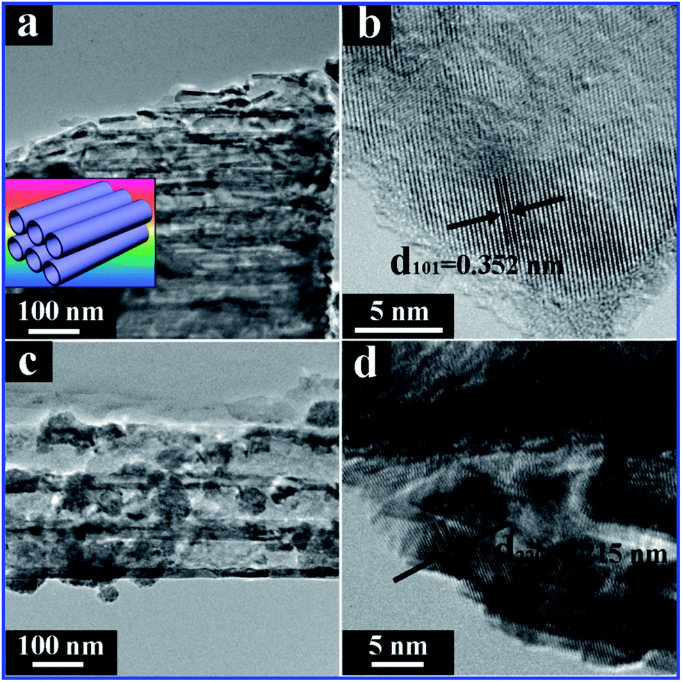 | ||
| Fig. 5 TEM images of (a) NP-TNTAs with corresponding stacking model in the inset and (c) CdSe/NP-TNTAs heterostructure. HRTEM images of (b) NP-TNTAs and (d) CdSe/NP-TNTAs heterostructure. | ||
3.2 Photoelectrochemical performances of the CdSe/NP-TNTAs heterostructure
Within a photoelectrochemical (PEC) water splitting cell, the equilibrium of the semiconductor's Fermi level with the redox potential of the electrolyte solution results in band bending. Therefore, the generation of an electrical field drives the photogenerated minority charges from the semiconductor (i.e. electrons from p-type semiconductors and/or holes from n-type semiconductors) toward the semiconductor/water interface, where water is either oxidized to oxygen by an n-type semiconductor (photoanode) or reduced to hydrogen with a p-type semiconductor (photocathode).41 Linear sweep photovoltammetry (LSV) measurements were first performed to determine the photocurrent densities of different samples under visible light irradiation (λ > 420 nm). As shown in Fig. 6a, notable photocurrent densities were recorded over the samples in the designated potential profile for PEC water splitting performance evaluation, which increases with the forward bias voltage, indicative of a typical n-type semiconductor.46 Specifically, the photocurrent density of the sample as a function of the applied bias voltage follows the order CdSe/NP-TNTAs > NP-TNTAs > CdSe film, and no photocurrent was observed over the samples in dark (Fig. S9†). The advantageous photocurrent of the CdSe/NP-TNTAs heterostructure over its counterparts, namely, blank NP-TNTAs and CdSe film, could be ascribed to the favorable energy level alignment between NP-TNTAs (TiO2) and CdSe (i.e. type II band alignment) and the intimate interfacial interaction afforded by the facile electrochemical deposition. Consistently, as revealed in Fig. 6b, the short-circuit transient photocurrent responses of the samples collected via amperometric I–t measurements demonstrate an analogous result, among which the CdSe/NP-TNTAs heterostructure shows the most enhanced photocurrent. It should be noted that upon light irradiation, the CdSe/NP-TNTAs heterostructure shows a steep rise of photocurrent followed by a transient decay, while blank NP-TNTAs shows a gradient increase of current. This may be caused by the intrinsic defect sites formed on the surface of CdSe, which may act as surface recombination centers for photogenerated electron–hole carriers and high internal resistance due to the system not being sufficiently mixed. Nevertheless, the transient photocurrent density of CdSe/NP-TNTAs heterostructures is still at least seven-fold higher than those of NP-TNTAs and CdSe film under visible light irradiation. Furthermore, a specific influence of the deposition time on the photocurrent densities of CdSe/NP-TNTAs heterostructures under varied applied bias voltages was also specifically probed (Fig. S10†), from which the optimal deposition time was determined to be 1600 s. It should be pointed out that the pure CdSe film shows the most unfavorable photocurrent density among the samples, which can be ascribed to the extremely fast recombination rate of photoexcited electron–hole pairs over the large CdSe aggregates deposited on the Ti foil (Fig. S5†). | ||
| Fig. 6 (a) Photocurrent–photovoltage (I–V) curves (5 mV s−1) and (b) zero-biased short-circuit transient photocurrent responses of NP-TNTAs, CdSe film and CdSe/NP-TNTAs heterostructure under on–off cycles of visible light irradiation (λ > 420 nm) in 1 M NaOH aqueous solution (pH = 13.9). (c) Illuminated open circuit potential and (d) electron lifetime determined from the decay of open circuit potential in dark. (e) Electrochemical impedance spectroscopy (EIS) Nyquist plots of samples with zero bias under visible light irradiation (λ > 420 nm), in which the amplitude of the sinusoidal wave was set at 10 mV and frequency varied from 100 kHz to 0.1 Hz in 1 M NaOH aqueous solution. (f) Mott–Schottky plots of NP-TNTAs and CdSe/NP-TNTAs heterostructure. | ||
To explore the origin of the significantly enhanced PEC performances of the CdSe/NP-TNTAs heterostructure, open circuit photovoltage decay (OCPD) and electrochemical impedance spectra (EIS) were investigated. It has been well established that the OCPD technique can be applied to assess the lifetime of photoelectrons and to evaluate the recombination rate of the photogenerated electron–hole charge carriers, which consists of turning off the illumination at a steady state and monitoring the subsequent decay of photovoltage (Voc) with time (Fig. 6c). The Voc decay rate is closely related to the photoelectron lifetime, as formulated by the following equation.61
| τ = (kBT/e)(dVoc/dt)−1 |
EIS, as a powerful tool to study the charge transfer process on the electrode and at the contact interface between the electrode and electrolyte, was utilized to probe the separation efficiency of the charge carriers.62 It should be emphasized that the EIS measurements conducted in our work were performed covering the frequency range of 105–0.1 Hz using an amplitude of 10 mV at the open circuit potential of the system. The semicircle in the Nyquist plots conveys information on the charge transfer process, in which the diameter of the semicircle corresponds to the charge transfer resistance.41Fig. 6e shows the Nyquist plots of different samples under visible light irradiation, in which the CdSe/NP-TNTAs heterostructure shows the smallest semicircular diameter among all the samples. Therefore, the result indicates that the CdSe/NP-TNTAs heterostructure possesses the smallest charge transfer resistance when compared with the other counterparts.
Fig. 6f shows the Mott–Schottky (M–S) plot with 1/C2versus potential. The slopes of the linear parts of the curves in the M–S plot are positive, suggesting typical n-type semiconductor behavior.48 The linear parts of the curves are extrapolated to 1/C2 → 0, and the values of the Fermi levels (UFLversus RHE) are estimated to be 0.310 V and 0.340 V for NP-TNTAs and the CdSe/NP-TNTAs heterostructure, respectively. The positive shift of UFL (ca. 30 mV) for the CdSe/NP-TNTAs heterostructure relative to NP-TNTAs indicates a decrease in the band bending edge resulting from the formation of the heterojunction nanocomposite,63 thus facilitating the electron transfer from CdSe to NP-TNTAs.41 As a consequence, the M–S result indicates that the CdSe/NP-TNTAs heterostructure shows a faster carrier transfer than NP-TNTAs, which results in the significantly enhanced PEC water splitting performances.
The carrier density (ND) over the samples can be determined from Fig. 6f according to the following equation:41
| ND = (2/eεε0) [dUFL/d(1/C2)] |
Incident photon-to-current conversion efficiency (IPCE) measurements have been carried out under zero-bias condition to investigate the origin of the photocurrent generation as a function of the incident light wavelength. As revealed in Fig. 7a, the IPCE spectrum of the CdSe/NP-TNTAs heterostructure is in agreement with its UV-vis spectrum, indicating a close relationship between the photocurrent and light absorption in the visible region. It was revealed that both blank NP-TNTAs and CdSe film show negligible IPCE (data not shown), which is consistent with their extremely low photocurrent profiles in Fig. 6b. On the contrary, the CdSe/NP-TNTAs heterostructure exhibits a pronounced photoresponse in the visible region (400–800 nm) with a maximum IPCE value of 0.45% at a wavelength of around 550 nm. The result suggests that the homogenous deposition of CdSe on the NP-TNTAs framework remarkably enhances the visible light absorption of the hybrid nanostructure, thereby giving rise to a significant enhancement in the IPCE and PEC performances.
 | ||
| Fig. 7 (a) Incident photon-to-current conversion efficiency (IPCE) curve of the CdSe/NP-TNTAs electrode, and (b) schematic illustration for CdSe/NP-TNTAs heterostructure as photoanode in PEC water splitting cell. | ||
Fig. 7b vividly depicts the PEC water splitting mechanism over the photoanode of CdSe/NP-TNTAs. The inset in Fig. 7b lists the specific energy diagram of the CdSe/NP-TNTAs hybrid nanostructure, for which both the conduction band minimum and valence band maximum of CdSe are located higher than those of NP-TNTAs, thus forming a typical type II band alignment. Consequently, the photogenerated electrons can be efficiently injected from CdSe to NP-TNTAs upon light irradiation, and flow toward the conducting Ti foil substrate along the vertical path afforded by self-organized NP-TNTAs, thereby leading to the significantly enhanced photoconversion efficiency.64 The analogous PEC mechanism can also be corroborated by the PEC performances of different samples under simulated solar light irradiation (Fig. S11†).
3.3 Photoredox performances of the CdSe/NP-TNTAs heterostructure
The photocatalytic performances of the samples were evaluated by the liquid-phase degradation of methyl orange (MO) aqueous solution, a model organic dye pollutant, under visible light (λ > 420 nm) irradiation. Blank experiments (i.e. without catalyst or visible light) show negligible photocatalytic activities (Fig. S12†), confirming that the degradation reaction is truly driven by a photocatalytic process. The photodegradation of an organic dye pollutant can be described by a pseudo-first-order reaction that follows the simplified Langmuir–Hinshelwood model, viz. ln(C0/C) = kat (when C0 is small), where ka is the apparent first-order rate constant.65 As shown in Fig. 8a, the CdSe/NP-TNTAs heterostructure exhibits remarkably enhanced photocatalytic performance in comparison with a blank CdSe film and NP-TNTAs, the order of which is in faithful agreement with the PEC result. Notably, the photocatalytic activity of the CdSe/NP-TNTAs heterostructure is also higher than that of the CdSe/TiO2 particulate film under the same experimental conditions, which can be ascribed predominantly to the hierarchically ordered nanostructure of NP-TNTAs, (i.e. periodically ordered nanorings on the surface and nanotubes in the bottom), which ensures much more efficient vectorial charge transfer along the long axis of nanotubes than that within the particulate film.8 Moreover, the larger specific surface area of 1-D NP-TNTAs scaffold as compared with randomly stacked TiO2 particulate film should not be ignored, which also facilitates more adsorption of the organic dye pollutant for photodegradation reaction.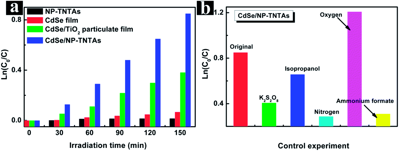 | ||
| Fig. 8 (a) Photocatalytic performances of different samples, and (b) photocatalytic performances of CdSe/NP-TNTAs heterostructure in the presence of O2, N2, ammonium formate (a scavenger for holes), isopropanol (a scavenger for hydroxyl radicals), and K2S2O8 (a scavenger for electrons) under ambient conditions, and irradiation time was restricted to 150 min. | ||
To further clarify the role of photogenerated radical species and underlying reaction mechanism involved for the photocatalytic processes under visible light irradiation, a collection of control experiments in N2 and O2 atmospheres, as well as with adding different scavengers for quenching hydroxyl radicals (˙OH), holes (h+), and electrons (e−), were carried out.66,67 As shown in Fig. 8b, a control experiment in an inert N2 atmosphere reveals remarkably lower photoactivity for the CdSe/NP-TNTAs heterostructure; however, an O2 atmosphere contributes towards the conspicuously enhanced photoactivity of the hybrid nanostructure, which suggests that an oxygen environment is beneficial for producing active species during the photocatalytic process. Moreover, it was found that when ammonium formate, isopropanol, and K2S2O8 were added into the reaction system as scavengers for holes, hydroxyl radicals, and electrons, respectively, the photocatalytic performances of the CdSe/NP-TNTAs heterostructure under visible light irradiation were concurrently prohibited. This suggests the synergistic catalytic role of electrons, hydroxyl radicals, and holes, among which the ammonium formate scavenger for holes exerts the most profound influence. It should be emphasized that, although photogenerated electrons are not able to directly participate in the reaction during the photocatalytic process, the electron quenching through the addition of K2S2O8 scavenger could prevent the activation of molecular oxygen dissolved in the aqueous solution and reduce a number of active species (e.g. hydroxyl or superoxide radicals), thus leading to the undesirable photocatalytic performances of the CdSe/NP-TNTAs heterostructure.67 Accordingly, the above control experiments ascertain that an O2 atmosphere along with holes plays the most important role in the photodegradation of organic dye pollutants over the CdSe/NP-TNTAs heterostructure, and hydroxyl radicals contribute partially to the enhancement.
The photoreduction performance of the CdSe/NP-TNTAs heterostructure was evaluated by the photocatalytic hydrogenation of an aromatic nitro compound (4-nitroaniline, 4-NA) to its corresponding amino organic (4-phenylenediamine, 4-PDA) in the aqueous phase under visible light irradiation.68–71 Blank experiments (without light or catalyst) under identical experimental conditions show negligible photoactivity, suggesting that the reaction was driven by a photocatalytic process (Fig. S13†). As shown in Fig. 9a, consistently, the CdSe/NP-TNTAs heterostructure shows optimal photoactivity toward the hydrogenation of 4-NA under visible light irradiation, and the photocatalytic performances of the samples follow the order CdSe/NP-TNTAs > CdSe/TiO2 particulate film > NP-TNTAs ≈ CdSe film, which shows an analogous result as revealed in Fig. 8a. Moreover, the cycling measurements reveal the favorable photostability of the CdSe/NP-TNTAs heterostructure (Fig. S14†). Notably, such a similar photoactivity enhancement has also been observed in other nitroaromatic compounds under the same visible light irradiation, such as 2-NA and 3-NA, as shown in Fig. S15.† With respect to the reduction reaction under visible light irradiation, the photocatalytic hydrogenation of 4-NA to 4-PDA was monitored by the UV-vis light absorption spectra.72 Prior to visible light irradiation, only one absorption peak at 380 nm corresponding to 4-NA was observed. Two new peaks at ca. 300 nm and 240 nm gradually arose with the progress of the reaction, which are attributed to the formation of 4-PDA, indicating the successful reduction of 4-NA to 4-PDA. The products of this reduction reaction under visible light irradiation have also been undoubtedly ascertained by high performance liquid chromatography (HPLC).68–71
 | ||
| Fig. 9 (a) Photocatalytic reduction of 4-NA over different samples under visible light irradiation (λ > 420 nm) with the addition of ammonium formate as quencher for photogenerated holes and N2 purge under ambient conditions. (b) Control experiments using K2S2O8 as electron scavenger for reduction of 4-NA over CdSe/NP-TNTAs heterostructure under visible light irradiation (λ > 420 nm) with the addition of ammonium formate as quencher for photogenerated holes and N2 purge under ambient conditions. | ||
To evaluate the role of photogenerated electrons in the photocatalytic reduction of aromatic nitro compounds, control experiments with and without the addition of K2S2O8 as an electron scavenger for photogenerated electrons in N2 atmosphere were performed. As shown in Fig. 9b, the photocatalytic reduction of 4-NA over the CdSe/NP-TNssaTAs heterostructure was remarkably retarded when K2S2O8 was introduced into the reaction system, which highlights the crucial role played by photogenerated electrons in driving the photocatalytic hydrogenation of aromatic nitro compounds.
3.4 Photocatalytic mechanism of the CdSe/NP-TNTAs heterostructure
Scheme 2 shows the separation process of photogenerated electron–hole pairs and photoredox reactions involved in the photocatalytic process over the CdSe/NP-TNTAs heterostructure. Specifically, when CdSe is irradiated by visible light, electrons are rapidly photoexcited from the valence band (VB) of CdSe to its conduction band (CB), leaving holes in the VB. The electrons can be readily injected from the CB of CdSe to the CB of TiO2 owing to the intimate interfacial interaction and favorable energy alignment between CdSe and NP-TNTAs (TiO2). In this way, various highly active species, such as hydroxyl radicals, hydrogen peroxide and superoxide radicals stemming from the reactions between electrons, oxygen, and water, were produced in situ, which collectively result in the significantly enhanced photoredox performances of the CdSe/NP-TNTAs heterostructure. Furthermore, notably, in terms of the NP-TNTAs framework, which is crystallized and self-aligned on the conducting Ti substrate, the injected electrons can be simultaneously transferred vertically to the bottom Ti foil, thereby contributing toward the separation of the electron–hole pairs and the significantly enhanced photoconversion efficiency.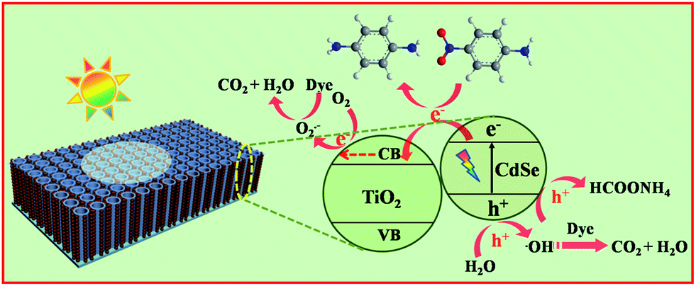 | ||
| Scheme 2 Schematic illustration showing the photocatalytic mechanism over CdSe/NP-TNTAs heterostructure. | ||
Moreover, with regard to the photocatalytic reduction of the aromatic nitro compound (4-NA) over a CdSe/NP-TNTAs composite system under visible light irradiation, photoexcited holes from the valence band (VB) of CdSe are completely quenched by the addition of ammonium formate, and the photogenerated electrons from the CB of CdSe flow toward the NP-TNTAs and react efficiently with the aromatic nitro compound adsorbed on the NP-TNTAs substrate, thereby fulfilling the photoreduction process. Moreover, it should be noted that the reaction was carried out under N2 purge, which prohibits the involvement of O2 in the reaction system and guarantees the complete reduction of the aromatic nitro compound by the photogenerated electrons.
4. Conclusions
In summary, a hierarchically ordered CdSe/NP-TNTAs heterostructure has been constructed by a facile electrochemical deposition strategy, by which CdSe nanocrystals were uniformly deposited on the NP-TNTAs framework. It was found that the well-defined CdSe/NP-TNTAs heterostructure can be utilized as an efficient photoanode for PEC water splitting under visible light irradiation and as a versatile visible-light-driven photocatalyst for photoredox applications, i.e. photooxidation of organic dye pollutants and the photocatalytic reduction of aromatic nitro compounds under ambient conditions. PEC and photocatalytic mechanisms over a CdSe/NP-TNTAs heterostructure were specifically explored, and the predominant active species responsible for the remarkably enhanced photocatalytic performances of the CdSe/NP-TNTAs binary nanocomposite were unequivocally ascertained. It is anticipated that our work may provide new insights in the fabrication of various hierarchically ordered narrow bandgap semiconductor/1-D semiconductor nanomaterials for extensive photocatalytic or PEC applications.Acknowledgements
This work was supported by the Nanyang Technological University startup grant: M4080977.120 and Singapore Ministry of Education Academic Research Fund (AcRF) Tier 1: M4011021.120. and Singapore-Berkeley Research Initiative for Sustainable Energy (SinBeRise).References
- Y. Zhang, Z.-R. Tang, X. Fu and Y.-J. Xu, ACS Nano, 2011, 5, 7426–7435 CrossRef CAS PubMed
.
- Z.-R. Tang, F. Li, Y. Zhang, X. Fu and Y.-J. Xu, J. Phys. Chem. C, 2011, 115, 7880–7886 CAS
- Y. Zhang, Z.-R. Tang, X. Fu and Y.-J. Xu, ACS Nano, 2010, 4, 7303–7314 CrossRef CAS PubMed
- M. A. Fox and M. T. Dulay, Chem. Rev., 1993, 93, 341–357 CrossRef CAS
- B. Liu and E. S. Aydil, J. Am. Chem. Soc., 2009, 131, 3985–3990 CrossRef CAS PubMed
- A. E. Mohamed and S. Rohani, Energy Environ. Sci., 2011, 4, 1065–1086 CAS
- Z. Zhang, R. Dua, L. B. Zhang, H. B. Zhu, H. N. Zhang and P. Wang, ACS Nano, 2013, 7, 1709–1717 CrossRef CAS PubMed
- K. Zhu, N. R. Neale, A. Miedaner and A. J. Frank, Nano Lett., 2007, 7, 69–74 CrossRef CAS PubMed
- P. Roy, S. Berger and P. Schmuki, Angew. Chem., Int. Ed., 2011, 50, 2904–2939 CrossRef CAS PubMed
- F. Xiao, Chem. Commun., 2012, 48, 6538–6540 RSC
- F. Xiao, J. Phys. Chem. C, 2012, 116, 16487–16498 CAS
- S. Liu, L. Yang, S. Xu, S. Luo and Q. Qai, Electrochem. Commun., 2009, 11, 1748–1751 CrossRef CAS PubMed
- Q. Li and J. K. Shang, Environ. Sci. Technol., 2009, 43, 8923–8929 CrossRef CAS PubMed
- S. K. Mohapatra, M. Misra, V. K. Mahajan and K. S. Raja, J. Phys. Chem. C, 2007, 111, 8677–8685 CAS
- N. Lu, X. Quan, J. Y. Li, S. Chen, H. T. Yu and G. H. Chen, J. Phys. Chem. C, 2007, 111, 11836–11842 CAS
- A. Ghicov, B. Schmidt, J. Kunze and P. Schmuki, Chem. Phys. Lett., 2007, 433, 323–326 CrossRef CAS PubMed
- F.-X. Xiao, J. Miao, H.-Y. Wang and B. Liu, J. Mater. Chem. A, 2013, 1, 12229–12238 CAS
- W. T. Sun, Y. Yu, H. Y. Pan, X. F. Gao, Q. Chen and L.-M. Peng, J. Am. Chem. Soc., 2008, 130, 1124–1125 CrossRef CAS PubMed
- S. Banerjee, S. K. Mohapatra, P. P. Das and M. Misra, Chem. Mater., 2008, 20, 6784–6791 CrossRef CAS
- I. Robel, V. Subramanian, M. Kuno and P. V. Kamat, J. Am. Chem. Soc., 2006, 128, 2385–2393 CrossRef CAS PubMed
- J. A. Seabold, K. Shankar, R. H. T. Wilke, M. Paulose, O. K. Varghese, C. A. Grimes and K. S. Choi, Chem. Mater., 2008, 20, 5266–5273 CrossRef CAS
- X.-F. Gao, H. B. Li, W. T. Sun, Q. Chen, F. Q. Tang and L. M. Peng, J. Phys. Chem. C, 2009, 113, 7531–7535 CAS
- R. Plass, S. Pelet, J. Krueger and M. Gratzel, J. Phys. Chem. B, 2002, 106, 7578–7580 CrossRef CAS
- L. M. Peter, K. G. U. Wijayantha, D. J. Riley and J. P. Waggett, J. Phys. Chem. B, 2003, 107, 8378–8381 CrossRef CAS
- A. Zaban, O. I. Micic, B. A. Gregg and A. J. Nozik, Langmuir, 1998, 14, 3153–3156 CrossRef CAS
- J. Y. Gan, T. Zhai, X. H. Lu, S. L. Xie, Y. C. Mao and Y. X. Tong, Mater. Res. Bull., 2012, 47, 580–585 CrossRef CAS PubMed
- L. X. Yang, S. L. Luo, R. H. Liu, Q. Y. Cai, Y. Xiao, S. H. Liu, F. Su and L. F. Wen, J. Phys. Chem. C, 2010, 114, 4783–4789 CAS
- J. G. Hensel, M. Wang, Y. Li and J. Z. Zhang, Nano Lett., 2010, 10, 478–483 CrossRef CAS PubMed
- G. Ai, W. T. Sun, X.-F. Gao, Y. L. Zhang and L.-M. Peng, J. Mater. Chem., 2011, 21, 8749–8755 RSC
- A. Kongkanand, K. Tvrdy, K. Takechi, M. Kuno and P. V. Kamat, J. Am. Chem. Soc., 2008, 130, 4007–4015 CrossRef CAS PubMed
- W. Lee, S. H. Kang, S. K. Min, Y.-E. Sung and S.-H. Han, Electrochem. Commun., 2008, 10, 1579–1582 CrossRef CAS PubMed
- H. Zhang, X. Quan, S. Chen, H. T. Yu and N. Ma, Chem. Mater., 2009, 21, 3090–3095 CrossRef CAS
- M. F. Hossain, S. Biswas, Z. H. Zhang and T. Takahashi, J. Photochem. Photobiol., A, 2011, 217, 68–75 CrossRef CAS PubMed
- K. Shin, S. IlSeok, S. H. Im and J. H. Park, Chem. Commun., 2010, 46, 2385–2387 RSC
- D. Pradhan and K. T. Leung, Langmuir, 2008, 24, 9707–9716 CrossRef CAS PubMed
- G. R. Li, X.-H. Lu, D.-L. Qu, C.-Z. Yao, F.-L. Zheng, Q. Bu, C.-R. Dawa and Y.-X. Tong, J. Phys. Chem. C, 2007, 111, 6678–6683 CAS
- N. Zhang and Y.-J. Xu, Chem. Mater., 2013, 25, 1979–1988 CrossRef CAS
- S. Liu, Z. Chen, N. Zhang, Z.-R. Tang and Y.-J. Xu, J. Phys. Chem. C, 2013, 117, 8251–8261 CAS
- N. Zhang, M.-Q. Yang, Z.-R. Tang and Y.-J. Xu, ACS Nano, 2014, 8, 623–633 CrossRef CAS PubMed
- B. Weng, S. Q. Liu, N. Zhang, Z.-R. Tang and Y.-J. Xu, J. Catal., 2014, 309, 146–155 CrossRef CAS PubMed
- Z. Zhang and P. Wang, Energy Environ. Sci., 2012, 5, 6506–6512 CAS
- Z. Zhang, M. F. Hossain and T. Takahashi, Int. J. Hydrogen Energy, 2010, 35, 8528–8535 CrossRef CAS PubMed
- G. Zhang, H. Huang, Y. Zhang, H. L. W. Chan and L. Zhou, Electrochem. Commun., 2007, 9, 2854–2858 CrossRef CAS PubMed
- F. Wang, Y. Liu, W. Dong, M. R. Shen and Z. H. Kang, J. Phys. Chem. C, 2011, 115, 14635–14640 CAS
- D. Wang, Y. Liu, C. W. Wang, F. Zhou and W. M. Liu, ACS Nano, 2009, 3, 1249–1257 CrossRef CAS PubMed
- F.-X. Xiao, J. Miao and B. Liu, Mater. Horiz., 2014, 1, 259–263 RSC
- Z. Zhang, L. B. Zhang, M. N. Hedhili, H. N. Zhang and P. Wang, Nano Lett., 2012, 13, 14–20 CrossRef PubMed
- M. Cocivera, A. Darkowski and B. Love, J. Electrochem. Soc., 1984, 131, 2514–2517 CrossRef CAS PubMed
- J. Miao, H. Yang, S.-Y. Khoo and B. Liu, Nanoscale, 2013, 5, 11118–11124 RSC
- Y.-J. Xu, Y. Zhuang and X. Fu, J. Phys. Chem. C, 2010, 114, 2669–2676 CAS
- H. C. Zeng, F. Xie, K. C. Wong and K. A. R. Mitchell, Chem. Mater., 2002, 14, 1788–1796 CrossRef CAS
- X. M. Wei and H. C. Zeng, Chem. Mater., 2003, 15, 433–442 CrossRef CAS
- M. A. Centeno, M. Paulis, M. Montes and J. A. Odriozola, Appl. Catal., B, 2005, 61, 177–183 CrossRef CAS PubMed
- J. Li, S. B. Tang, L. Lu and H. C. Zeng, J. Am. Chem. Soc., 2007, 129, 9401–9409 CrossRef CAS PubMed
- J. Li and H. C. Zeng, Chem. Mater., 2006, 18, 4270–4277 CrossRef CAS
- O. I. Micic, M. T. Nenadovic, M. W. Peterson and A. J. Nozik, J. Phys. Chem., 1987, 91, 1295–1297 CrossRef CAS
- X. T. Pian, B. Z. Lin, Y. L. Chen, J. D. Kuang, K. Z. Zhang and L. M. Fu, J. Phys. Chem. C, 2011, 115, 6531–6539 CAS
- J. Zhang, J. G. Yu, M. Jaroniec and J. R. Gong, Nano Lett., 2012, 12, 4584–4589 CrossRef CAS PubMed
- L. J. Meng, H. Meng, W. J. Gong, W. Liu and Z. D. Zhang, Thin Solid Films, 2011, 519, 7627–7631 CrossRef CAS PubMed
- T. Takahashi, T. Sagawa and H. Hamanaka, J. Non-Cryst. Solids, 1984, 65, 261–267 CrossRef CAS
- B. H. Meekins and P. V. Kamat, ACS Nano, 2009, 3, 3437–3446 CrossRef CAS PubMed
- N. Li, G. Liu, C. Zhen, F. Li, L. L. Zhang and H. M. Cheng, Adv. Funct. Mater., 2011, 21, 1717–1722 CrossRef CAS
- P. K. Ghosh and M. E. Azimi, IEEE Trans. Dielectr. Electr. Insul., 1994, 1, 975–981 CrossRef
- P. V. Kamat, J. Phys. Chem. C, 2008, 112, 18737–18753 CAS
- Y. Zhang, N. Zhang, Z.-R. Tang and Y.-J. Xu, ACS Nano, 2012, 6, 9777–9789 CrossRef CAS PubMed
- Y. Zhang, N. Zhang, Z.-R. Tang and Y.-J. Xu, Chem. Sci., 2013, 4, 1820–1824 RSC
- M.-Q. Yang, Y. Zhang, N. Zhang, Z.-R. Tang and Y.-J. Xu, Sci. Rep., 2013, 3, 3314–3320 Search PubMed
- M.-Q. Yang, B. Weng and Y.-J. Xu, J. Mater. Chem. A, 2014, 2, 1710–1720 CAS
- S. Liu and Y.-J. Xu, Nanoscale, 2013, 5, 9330–9339 RSC
- M.-Q. Yang, B. Weng and Y.-J. Xu, Langmuir, 2013, 29, 10549–10558 CrossRef CAS PubMed
- M.-Q. Yang and Y.-J. Xu, Phys. Chem. Chem. Phys., 2013, 15, 19102–19118 RSC
- F.-X. Xiao, J. Miao and B. Liu, J. Am. Chem. Soc., 2014, 136, 1559–1569 CrossRef CAS PubMed
Footnote |
| † Electronic supplementary information (ESI) available. See DOI: 10.1039/c4nr01380h |
| This journal is © The Royal Society of Chemistry 2014 |