Current transport in graphene/AlGaN/GaN vertical heterostructures probed at nanoscale†
Abstract
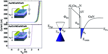
Vertical heterostructures combining two or more graphene (Gr) layers separated by ultra-thin insulating or semiconductor barriers represent very promising systems for next generation electronics devices, due to the combination of high speed operation with wide-range current modulation by a gate bias. They are based on the specific mechanisms of current transport between two-dimensional-electron-gases (2DEGs) in close proximity. In this context, vertical devices formed by Gr and semiconductor heterostructures hosting an “ordinary” 2DEG can be also very interesting. In this work, we investigated the vertical current transport in Gr/Al0.25Ga0.75N/GaN heterostructures, where Gr is separated from a high density 2DEG by a ∼24 nm thick AlGaN barrier layer. The current transport from Gr to the buried 2DEG was characterized at nanoscale using conductive atomic force microscopy (CAFM) and scanning capacitance microscopy (SCM). From these analyses, performed both on Gr/AlGaN/GaN and on AlGaN/GaN reference samples using AFM tips with different metal coatings, the Gr/AlGaN Schottky barrier height ΦB and its lateral uniformity were evaluated, as well as the variation of the carrier densities of graphene (ngr) and AlGaN/GaN 2DEG (ns) as a function of the applied bias. A low Schottky barrier (∼0.40 eV) with excellent spatial uniformity was found at the Gr/AlGaN interface, i.e., lower compared to the measured values for metal/AlGaN contacts, which range from ∼0.6 to ∼1.1 eV depending on the metal workfunction. The electrical behavior of the Gr/AlGaN contact has been explained by Gr interaction with AlGaN donor-like surface states located in close proximity, which are also responsible of high n-type Gr doping (∼1.3 × 1013 cm−2). An effective modulation of ns by the Gr Schottky contact was demonstrated by capacitance analysis under reverse bias. From this basic understanding of transport properties in Gr/AlGaN/GaN heterostructures, novel vertical field effect transistor concepts with high operating speed and Ion/Ioff ratio can be envisaged.
 Please wait while we load your content...

