 Open Access Article
 This Open Access Article is licensed under a Creative Commons Attribution-Non Commercial 3.0 Unported Licence
van der Waals trilayers and superlattices: modification of electronic structures of MoS2 by intercalation†
Ning Lu‡
ab,
Hongyan Guo‡cb,
Lu Wangcd,
Xiaojun Wuce and
Xiao Cheng Zeng*be
aCenter for Nano Science and Technology, Department of Physics, Anhui Normal University, Wuhu, Anhui 241000, China
bDepartment of Chemistry and Department Mechanics and Materials Engineering, University of Nebraska-Lincoln, Lincoln, NE 68588, USA. E-mail: xzeng1@unl.edu
cCAS Key Lab of Materials for Energy Conversion, Department of Materials Science and Engineering, University of Science and Technology of China, Hefei, Anhui 230026, China
dDepartment of Physics, University of Nebraska-Omaha, Omaha, NE 68182, USA
eHefei National Laboratory for Physical Sciences at the Microscale, University of Science and Technology of China, Hefei, Anhui 230026, China
First published on 4th March 2014
Abstract
We perform a comprehensive first-principles study of the electronic properties of van der Waals (vdW) trilayers via intercalating a two-dimensional (2D) monolayer (ML = BN, MoSe2, WS2, or WSe2) between a MoS2 bilayer to form various MoS2/ML/MoS2 sandwich trilayers. We find that the BN monolayer is the most effective sheet to decouple the interlayer vdW coupling of the MoS2 bilayer, and the resulting sandwich trilayer can recover the electronic structures of the MoS2 monolayer, particularly the direct-gap character. Further study of the MoS2/BN superlattices confirms the effectiveness of the BN monolayer for the decoupling of the MoS2–MoS2 interaction. In addition, the intercalation of a transition-metal dichalcogenide (TMDC) MoSe2 or WSe2 sheet makes the sandwich trilayer undergo an indirect-gap to direct-gap transition due to the newly formed heterogeneous S/Se interfaces. In contrast, the MoS2/WS2/MoS2 sandwich trilayer still retains the indirect-gap character of the MoS2 bilayer due to the lack of the heterogeneous S/Se interfaces. Moreover, the 3D superlattice of the MoS2/TMDC heterostructures also exhibits similar electronic band characters to the MoS2/TMDC/MoS2 trilayer heterostructures, albeit a slight decrease of the bandgap compared to the trilayers. Compared to the bulk MoS2, the 3D MoS2/TMDC superlattice can give rise to new and distinctive properties. Our study offers not only new insights into electronic properties of the vdW multilayer heterostructures but also guidance in designing new heterostructures to modify electronic structures of 2D TMDC crystals.
Introduction
Many experiments have demonstrated that two-dimensional (2D) transition-metal dichalcogenides (TMDCs) such as 2D MoS2 and WS2 crystals possess novel electronic,1–4 optical,5–8 catalytic,9,10 and mechanical properties.11–14 For example, electronic properties of 2D MoS2 crystals can be sensitive to the number of layers, that is, the MoS2 monolayer exhibits a direct bandgap with a value of ∼1.8 eV while a bilayer MoS2 exhibits an indirect bandgap with a value of ∼1.5 eV.15 As a result, significant enhancement of photoluminescence has been observed when MoS2 is thinned to a single layer.8,14 Previous study has also shown that when the MoS2 bilayer is pulled apart into two separated monolayers, the direct transition (K–K) is insensitive to the separation while the indirect transition (Γ–K) increases dramatically.16 It seems that the distance between the two monolayers or the interlayer vdW interaction can notably affect the electronic structures of two-dimensional (2D) layered TMDCs. Thus, one may ask two closely related questions: “can the MoS2 bilayer be effectively decoupled via intercalation of a 2D sheet without being pulled far too apart?” or “To what extent, can the intercalation of a 2D sheet affect electronic properties of the MoS2 bilayer?” The intercalation of a 2D sheet into the MoS2 bilayer gives rise to a hybrid trilayer, coined as the vdW heterostructures by Geim and Grigorieva.17 Recently, successful fabrication of multilayer vdW heterostructures by stacking one layer on top of another in a precisely controlled sequence has been demonstrated experimentally.18–20 The artificial vdW heterostructures can exhibit new and unusual properties that differ from their own constituent layers. For example, the vertical field-effect transistor and memory cell made of TMDC/graphene heterostructures19,21–23 as well as layered hybrids of MoS2 and WS2 have been realized in the laboratory.24 Previous theoretical studies suggest that the direct-gap character of the MoS2 monolayer can be retained in certain MoS2 heterobilayer structures whose electronic properties can be further tuned by an in-plane strain or a vertical electric field.25–29 In addition, the insulating BN monolayer is a good substrate for protecting high quality graphene electronics.30 A type-I band alignment for the BN monolayer and MoS2 monolayer is also reported.25 3D heterostructures such as superlattices are predicted to possess new properties that differ from their corresponding bulk structures, thereby opening a new way of materials design.31The focus of this study is to investigate effects of intercalation of either an insulating BN monolayer or a semiconducting TMDC monolayer (MoSe2, WS2, or WSe2) into a MoS2 bilayer on the electronic properties of the vdW trilayer heterostructure and the corresponding vdW superlattice. Our computational results suggest that the BN monolayer is an ideal sheet to decouple the MoS2 bilayer while a MoSe2 or WSe2 sheet can turn the indirect-gap of the MoS2 bilayer into a direct-gap trilayer.
Computational methods
All calculations are performed within the framework of spin-polarized plane-wave density functional theory (PW-DFT), implemented in the Vienna ab initio simulation package (VASP 5.3).32,33 The Perdew–Burke–Ernzerhof (PBE) functional and projector augmented wave (PAW) potentials are used.34–36 The effect of vdW interaction is accounted for by using the dispersion corrected DFT (optB88-vdW functional).37,38 The vacuum length between two adjacent images in the supercell is longer than 15 Å. An energy cutoff of 500 eV is adopted for the plane-wave expansion of the electronic wave function. Geometric structures are relaxed until the force on each atom is less than 0.01 eV Å−1 and the convergence criteria for energy is 1 × 10⁻⁵ eV.Note that the optimized MoS2 monolayer exhibits a cell parameter of 3.18 Å, while the cell parameter of a h-BN monolayer is 2.52 Å, in good agreement with previous results.39,40 As such, the 5 × 5 BN supercell almost perfectly matches the 4 × 4 MoS2 supercell with the lattice mismatch less than 1%. For the MoS2/BN/MoS2 trilayer, the supercell is fixed while the atomic coordinates are relaxed. For other sandwich systems containing TMDC MoSe2, WS2, or WSe2, a 1 × 1 cell is used due to the fact that their lattice parameters are close to that of MoS2. In these cases, both the cell length and atomic coordinates are relaxed to obtain the lattice parameters at the lowest total energy. Bader's atom in molecule (AIM) method based on charge density topological analysis is used for computing charge population.41 Once the optimized structures are obtained, a hybrid functional in the Heyd–Scuseria–Ernzerhof (HSE06) form is used to give more accurate bandgaps.42 The spin–orbit (SO) interaction is included in all the band-structure calculations.43
Results and discussion
Intercalation of a MoS2 bilayer with a BN monolayer
First, DFT/PBE calculations show that monolayer MoS2 is a semiconductor with a direct bandgap of 1.60 eV (see Table 1), in agreement with previous calculation.29 The MoS2 bilayer with the most stable C7 stacking, however, is a semiconductor with an indirect bandgap of 1.31 eV. HSE06 calculation enlarges the bandgaps of monolayer and bilayer MoS2 to 2.06 and 1.81 eV, respectively. For the BN monolayer, PBE calculation shows it is a semiconductor with a wide bandgap of 4.66 eV (Table 2).| ML-MoS2 | BL-MoS2 | A1B1A1 | A1B2A1 | A1B1A2 | A1B1A3 | SL-A1B1 | SL-A1B2 | |
|---|---|---|---|---|---|---|---|---|
| d | — | 3.09 | 3.36 | 3.36 | 3.36 | 3.36 | 3.35 | 3.35 |
| E BE | — | 0.22 | 0.36 | 0.36 | 0.37 | 0.36 | 0.38 | 0.38 |
| E g (PBE) | 1.60 | 1.31-indirect | 1.58 | 1.58 | 1.58 | 1.58 | 1.69 | 1.69 |
| E g (HSE06) | 2.06 | 1.81-indirect | 2.00 | — | — | — | — | — |
| ABA (B = MoSe2) | ACA (C = MoSe2) | ABA (B = WS2) | ACA (C = WS2) | ABA (B = WSe2) | ACA (C = WSe2) | |
|---|---|---|---|---|---|---|
| E g (PBE) | 0.70 | 0.75 | 1.05 (Γ–k) | 1.08 (Γ–k) | 0.39 | 0.42 |
| E g (HSE) | 0.97 | 1.02 | 1.47 (Γ–k) | 1.49 (Γ–k) | 0.61 | 0.64 |
| E g (PBE)_SL | 0.62 (Γ–k) | 0.59 (Γ–k) | 0.95 (Γ–k) | 0.93 (Γ–k) | 0.30 | 0.35 |
| E g (HSE)_SL | 0.88 | 0.92 | 1.35 (Γ–k) | 1.33 (Γ–k) | 0.50 | 0.54 |
Next, various MoS2/BN/MoS2 trilayer systems are built for which the lateral locations of the MoS2 monolayer and BN monolayer in different supercells are shown in Fig. 1. Specifically, we consider four different stacking orders: A1B1A1, A1B2A1, A1B1A2, and A1B1A3. PBE optimizations show that the total-energy differences among these configurations are typically less than 0.01 eV per formula cell, and the different stacking orders have little effect on the electronic structures. The binding energy of a trilayer, which measures the interlayer vdW interaction per supercell, is defined as: EBE = 2EMoS2 + EBN − EMoS2/BN/MoS2, where EMoS2 is the total energy of a MoS2 monolayer, EBN is the total energy of a BN monolayer, and EMoS2/BN/MoS2 is the total energy of a MoS2/BN/MoS2 trilayer. As listed in Table 1, the computed binding energies of the MoS2/BN/MoS2 heterostructure with A1B1A1, A1B2A1, A1B1A2, and A1B1A3 stacking orders are 0.36 eV, 0.36 eV, 0.37 eV, and 0.36 eV, respectively, reflecting the weak vdW interaction between the MoS2 layer and BN layer. Taking the A1B1A1 stacking as an example, its electronic structure is shown in Fig. 2c. Clearly, the trilayer retains the direct-gap character of the MoS2 monolayer. The computed bandgap is 1.58 eV, and both the conduction band minimum (CBM) and valence band maximum (VBM) are located at the K points, both contributed by the MoS2 layers. Like the PBE calculation, the HSE06 calculation also suggests a direct-gap character but the bandgap increases to 2.00 eV (ESI Fig. S1†). Overall, the intercalated BN layer has little effect on the band edge of MoS2 layers. To further confirm this conclusion, we remove the BN layer but leave the two MoS2 layers fixed at the original locations of the trilayer. As shown in Fig. 2b, again, the computed band structure shows a direct-gap character with the bandgap being 1.59 eV, very close to that of the MoS2/BN/MoS2 trilayer.
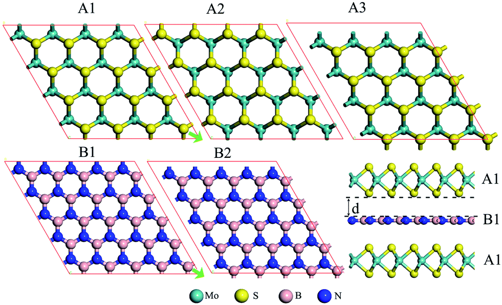 | ||
| Fig. 1 Top view of a MoS2 monolayer in three different supercells (marked by the red parallelogram) and a BN monolayer in two different supercells. A3 (B2) can be viewed as a displacement of A1 (B1) in the green-arrow direction shown in A1 (B1). Superimposing the ABA supercells allows us to build different MoS2/BN/MoS2 trilayers. An example of A1B1A1 trilayer is shown in the lower right panel. | ||
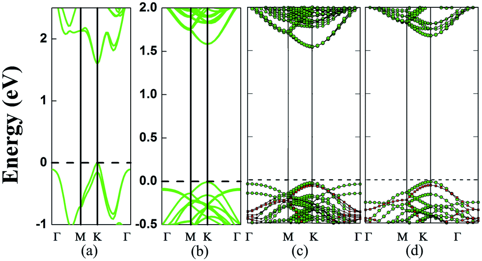 | ||
| Fig. 2 Computed electronic band structures (PBE) of (a) monolayer MoS2; (b) MoS2/vacuum layer/MoS2 by removing the BN layer from the MoS2/BN/MoS2 trilayer counterpart (in (c)) but with the fixed vertical location of the two MoS2 layers; (c) MoS2/BN/MoS2 with the A1B1A1 stacking; and (d) a 3D superlattice of MoS2/BN with the AB stacking. The green lines represent MoS2 layers while the red lines represent BN monolayer. | ||
We also compute the effective mass at the K point corresponding to the MoS2 monolayer and A1B1A1 trilayer, respectively. The directional dependence of the effective mass at the K point is small. For the MoS2 monolayer, m*e = 0.44m0 for the electron at CBM and m*h = 0.55m0 for the hole at VBM are in agreement with the previous studies.4,44 For A1B1A1, m*e = 0.44m0 and m*h = 0.59m0, similar to those of the monolayer, which indicates that the carrier mobility of the monolayer is also retained by the trilayer.
To confirm that the BN monolayer is an ideal sheet to decouple the interlayer coupling of the MoS2 bilayer, we also compute electronic structures of the 3D superlattice of hybrid BN/MoS2 layers. A superlattice with two different stacking orders (A1B1 and A1B2) of MoS2 and BN layers is considered and our calculations show that the two stacking orders give nearly the same results. For both stacking orders, the optimized cell parameters are a = b = 12.62 Å and c = 9.86 Å. As shown in Fig. 2d, the superlattice exhibits a direct gap of 1.69 eV, and both the VBM and CBM are located at the K point and both are contributed by MoS2 layers as in the case of the MoS2/BN/MoS2 trilayer system. The slightly enhanced bandgap compared to the trilayer system is largely due to a slight reduction of the cell parameters a and b. In summary, results of both the vdW trilayer and superlattice show that the alternatively stacked BN and MoS2 monolayers can retain the direct-gap character of the MoS2 monolayer. In other words, the BN monolayer is an effective divider to decouple the interlayer coupling for MoS2.
Intercalation of a MoS2 bilayer by MoSe2, WS2 or WSe2 monolayer
Previous experimental and theoretical studies demonstrate that the MoS2 bilayer is a semiconductor with an indirect bandgap.27,29,45 Recent theoretical studies of TMDC heterobilayers also show that the interlayer interaction due to heterointerfaces (e.g., S/Se) can notably affect the electronic properties. Thus, it is interesting to study the extent to which the intercalation of a heterogeneous TMDC monolayer between two MoS2 bilayers affects the electronic properties.Previous theoretical studies show that the C7 and T stacking patterns give the lowest energy for many heterobilayers,27,29 and the electronic structure is more or less the same with different stacking orders. Here, we adopt two different stacking orders for the trilayers (see Fig. 3), namely, the ABA and ACA. For the ABA trilayer, the interface AB is in C7 stacking, while for the ACA trilayer, the interface AC is in T stacking. Again, we find that the two stacking orders give rise to nearly the same electronic properties.
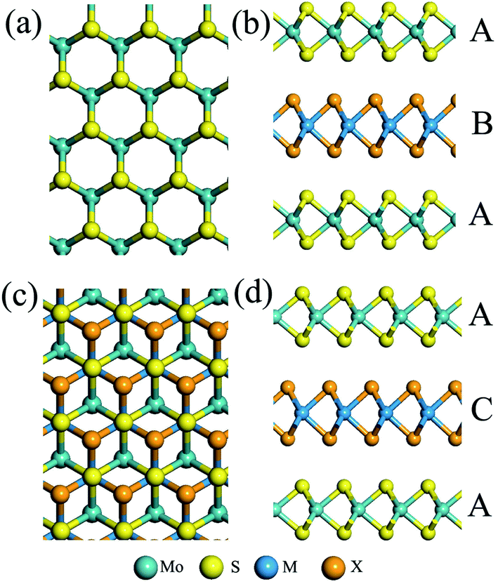 | ||
| Fig. 3 Top and side views of MoS2/MX2/MoS2 (M = Mo, W; X = S, Se) trilayers with (a and b) ABA stacking with a C7 interface and (c and d) ACA stacking with a T interface, respectively. | ||
The polarization within the S/Se interfaces is responsible for the direct-gap character of heterobilayers in previous studies.26,27 The MoS2/MoSe2/MoS2 trilayer entails two S/Se interfaces. In view of the MoS2 bilayer possessing an indirect bandgap, the intercalation of the MoSe2 monolayer induces an indirect to direct transition. As shown in Fig. 4a, the MoS2/MoSe2/MoS2 trilayer exhibits a direct bandgap of 0.69 eV. The VBM is located at the K point and is mainly contributed by the MoSe2 layer, while the CBM is also located at the K point and is mainly contributed by MoS2 layers. It is desirable that CBM and VBM are contributed from two different TMDC monolayers, particularly for the electron–hole separation. ESI (Fig. S2†) shows a more accurate HSE06 computation of band structures of the trilayers. The computed bandgap is 0.97 eV, wider than that from PBE computation. However, the electronic structures and the VBM and CBM are similar to those based on PBE computation.
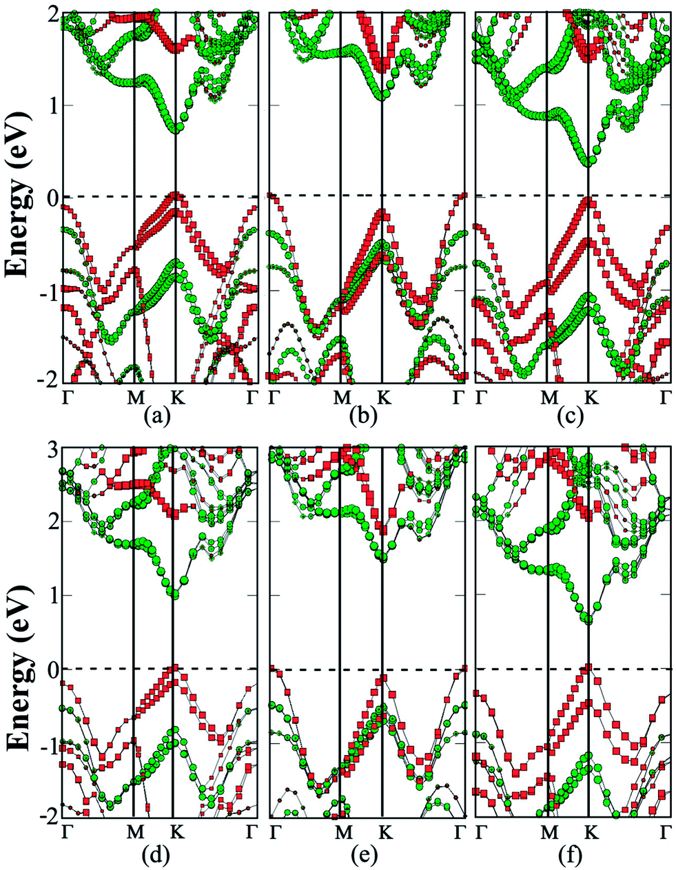 | ||
| Fig. 4 Computed band structures (PBE) of (a) MoS2/MoSe2/MoS2, (b) MoS2/WS2/MoS2, and (c) MoS2/WSe2/MoS2 trilayer with ABA stacking, respectively. Computed band structures (PBE) of (d) MoS2/MoSe2 superlattice, (e) MoS2/WS2 superlattice, and (f) MoS2/WSe2 superlattice with the AB stacking, respectively. The green lines mark contribution from MoS2 layers while the red lines mark contribution from the MoSe2, WS2 or WSe2 layer. | ||
Because of the lack of the S/Se interfaces, as shown in Fig. 4b, the MoS2/WS2/MoS2 trilayer still exhibits an indirect gap of 1.05 eV. The VBM is located at the Γ point and is mainly contributed by the WS2 monolayer, while the CBM is located at the K point and is mainly contributed by the two MoS2 layers. Computed band structures based on the HSE06 functional is shown in ESI Fig. S2.† Again, the trilayer still exhibits the indirect-gap character but the bandgap increases to 1.47 eV.
The MoS2/WSe2/MoS2 trilayer still exhibits a direct gap of 0.39 eV due to the presence of the two Se/S interfaces (see Fig. 4c). The VBM at the K point is mainly contributed by the WSe2 layer, while the CBM at the K point is mainly contributed by MoS2 layers. Again, as shown in ESI Fig. S2,† HSE06 calculation confirms the main character of electronic properties. To further analyze the effect of the polarization within the Se/S interfaces, charge transfer between neighboring layers is computed (see ESI Table S1†). For MoS2/MoSe2/MoS2 and MoS2/WSe2/MoS2 trilayers, a 0.02 e per unit cell is transferred from the MoSe2 (or WSe2) layer to the MoS2 layer. In contrast, for the MoS2/WS2/MoS2 trilayer with S/S interfaces, the charge transfer between two neighboring layers is nearly zero. This result further demonstrates that the interfacial polarization has an important effect on the electronic properties of the trilayer heterostructures.
Lastly, we consider a 3D superlattice made of hybrid MoS2 monolayers and other monolayers. As shown in Fig. 4, for each superlattice, two stacking orders including AB with a C7 interface and AC with a T interface are investigated. The binding energies and cell parameters for the AB and AC stacking are close to one another in all the configurations (see ESI Table S1†). For the MoS2/MoSe2 superlattice, PBE calculations suggest that its bandgap is still indirect, with a value of 0.62 and 0.59 eV respectively, for the AB and AC stacking. The bandgap is about 0.1 eV less than that of the corresponding trilayer. The CBM is still located at the K point and contributed mainly by the MoS2 layers (Fig. 4d), while the VBM energy at the Γ and K point differs only by 10 meV, and is mainly contributed by the MoSe2 layers. On the other hand, the HSE06 calculations suggest that the MoS2/MoSe2 superlattice is a direct-gap semiconductor with a value of 0.88 and 0.92 eV, respectively, for the AB and AC stacking. Here, the VBM energy in the K point is 77 meV lower than the Γ point (ESI Fig. S2†). For the MoS2/WS2 superlattice, both PBE and HSE06 calculations suggest that it is an indirect-gap semiconductor (Fig. 4e) with a bandgap value 0.95 and 1.35 eV, respectively, for the AB stacking. Finally, both PBE and HSE06 calculations suggest that the MoS2/WSe2 superlattice is a direct-gap semiconductor with a value of 0.3 and 0.5 eV for the AB stacking, and 0.35 and 0.54 eV for the AC stacking. Both bandgaps are smaller than those of the corresponding trilayers. Again, the bandgap reduction is mainly due to a slightly enlarged cell parameter (see ESI Table S1†).
Conclusions
In conclusion, our first-principles calculations show that the BN monolayer is a highly effective single sheet to decouple the interlayer vdW interaction of the MoS2 bilayer. The resulting vdW trilayer heterostructure can recover the electronic structures of a single MoS2 monolayer, particularly its direct-gap character. Further study of the 3D MoS2/BN superlattices confirms the effectiveness of the BN monolayer for decoupling the interlayer interaction. Expectedly, this conclusion has implications to MoS2 based heterostructures as well as to other TMDC-based vdW heterostructures. We have also investigated intercalation of a TMDC MoSe2 or WSe2 sheet between two MoS2 sheets and found that the resulting vdW trilayer undergoes an indirect-gap to direct-gap transition due to the newly formed heterogeneous S/Se interfaces. In contrast, the MoS2/WS2/MoS2 vdW trilayer still retains the indirect-gap character of the MoS2 bilayer due to the lack of the heterogeneous S/Se interfaces. Again, the 3D superlattice of the MoS2/TMDC heterostructures also exhibits similar electronic band characters to the MoS2/TMDC/MoS2 trilayer, albeit a slight decrease of the bandgap than that of their trilayer counterparts. In view of recent successful fabrication of vdW heterostructures by stacking a graphene sheet on top of MoS2 sheets or vice versa,19 the vdW trilayers and superlattices investigated in this study together with their novel properties may be tested in the laboratory in the near future.Acknowledgements
XCZ is grateful for valuable discussions with Professors Ali Adibi, Eric Vogel, Joshua Robinson, and Ali Eftekhar. The USTC group is supported by the National Basic Research Programs of China (nos 2011CB921400 and 2012CB 922001), NSFC (grant nos 21121003, 11004180, and 51172223), and One Hundred Person Project of CAS, Strategic Priority Research Program of CAS (XDB01020300). The UNL group is supported by ARL (grant no. W911NF1020099), NSF (grant no. DMR-0820521), UNL Nebraska Center for Energy Sciences Research, University of Nebraska Holland Computing Center, and a grant from USTC for (1000plan) Qianren-B summer research.References
- B. Radisavljevic, A. Radenovic, J. Brivio, V. Giacometti and A. Kis, Nat. Nanotechnol., 2011, 6, 147–150 CrossRef CAS PubMed
.
- H. Wang, L. L. Yu, Y. H. Lee, Y. M. Shi, A. Hsu, M. L. Chin, L. J. Li, M. Dubey, J. Kong and T. Palacios, Nano Lett., 2012, 12, 4674–4680 CrossRef CAS PubMed
- B. Radisavljevic, M. B. Whitwick and A. Kis, ACS Nano, 2011, 5, 9934–9938 CrossRef CAS PubMed
- Y. Yoon, K. Ganapathi and S. Salahuddin, Nano Lett., 2011, 11, 3768–3773 CrossRef CAS PubMed
- K. F. Mak, C. Lee, J. Hone, J. Shan and T. F. Heinz, Phys. Rev. Lett., 2010, 105, 136805 CrossRef PubMed
- K. F. Mak, K. He, C. Lee, G. H. Lee, J. Hone, T. F. Heinz and J. Shan, Nat. Mater., 2012, 12, 207–211 CrossRef PubMed
- D. Xiao, G.-B. Liu, W. Feng, X. Xu and W. Yao, Phys. Rev. Lett., 2012, 108, 196802 CrossRef PubMed
- A. Splendiani, L. Sun, Y. Zhang, T. Li, J. Kim, C.-Y. Chim, G. Galli and F. Wang, Nano Lett., 2010, 10, 1271–1275 CrossRef CAS PubMed
- D. Voiry, M. Salehi, R. Silva, T. Fujita, M. Chen, T. Asefa, V. B. Shenoy, G. Eda and M. Chhowalla, Nano Lett., 2013, 13, 6222–6227 CrossRef CAS PubMed
- H. L. Zhuang and R. G. Hennig, Chem. Mater., 2013, 25, 3232–3238 CrossRef CAS
- S. Bertolazzi, J. Brivio and A. Kis, ACS Nano, 2011, 5, 9703–9709 CrossRef CAS PubMed
- J. Pu, Y. Yomogida, K.-K. Liu, L.-J. Li, Y. Iwasa and T. Takenobu, Nano Lett., 2012, 12, 4013–4017 CrossRef CAS PubMed
- Y. Li, Z. Zhou, S. Zhang and Z. Chen, J. Am. Chem. Soc., 2008, 130, 16739–16744 CrossRef CAS PubMed
- K. F. Mak, C. Lee, J. Hone, J. Shan and T. F. Heinz, Phys. Rev. Lett., 2010, 105, 136805 CrossRef PubMed
- H. J. Conley, B. Wang, J. I. Ziegler, R. F. Haglund, S. T. Pantelides and K. I. Bolotin, Nano Lett., 2013, 13, 3626–3630 CrossRef CAS PubMed
- E. S. Kadantsev and P. Hawrylak, Solid State Commun., 2012, 152, 909–913 CrossRef CAS
- A. Geim and I. Grigorieva, Nature, 2013, 499, 419–425 CrossRef CAS PubMed
- L. Ponomarenko, A. Geim, A. Zhukov, R. Jalil, S. Morozov, K. N. I. Grigorieva, E. Hill, V. Cheianov, V. Fal'ko and K. Watanabe, Nat. Phys., 2011, 7, 958–961 CrossRef CAS
- L. Britnell, R. Gorbachev, R. Jalil, B. Belle, F. Schedin, A. Mishchenko, T. Georgiou, M. Katsnelson, L. Eaves and S. Morozov, Science, 2012, 335, 947–950 CrossRef CAS PubMed
- S. Haigh, A. Gholinia, R. Jalil, S. Romani, L. Britnell, D. Elias, K. Novoselov, L. Ponomarenko, A. Geim and R. Gorbachev, Nat. Mater., 2012, 11, 764–767 CrossRef CAS PubMed
- S. Bertolazzi, D. Krasnozhon and A. Kis, ACS Nano, 2013, 7, 3246–3252 CrossRef CAS PubMed
- T. Georgiou, R. Jalil, B. D. Belle, L. Britnell, R. V. Gorbachev, S. V. Morozov, Y.-J. Kim, A. Gholinia, S. J. Haigh and O. Makarovsky, Nat. Nanotechnol., 2013, 8, 100–103 CrossRef CAS PubMed
- W. J. Yu, Z. Li, H. Zhou, Y. Chen, Y. Wang, Y. Huang and X. Duan, Nat. Mater., 2012, 12, 246–252 CrossRef PubMed
- A. Anto Jeffery, C. Nethravathi and M. Rajamathi, J. Phys. Chem. C, 2013, 118, 1386–1396 Search PubMed
- H.-P. Komsa and A. V. Krasheninnikov, Phys. Rev. B: Condens. Matter Mater. Phys., 2013, 88, 085318 CrossRef
- H. Terrones, F. López-Urías and M. Terrones, Sci. Rep., 2013, 3, 1549 Search PubMed
-
(a) N. Lu, H. Guo, L. Li, J. Dai, L. Wang, W.-N. Mei, X. Wu and X. C. Zeng, Nanoscale, 2014, 6, 2879–2886 RSC
-
(a) Y. Ma, Y. Dai, M. Guo, C. Niu and B. Huang, Nanoscale, 2011, 3, 3883–3887 RSC
- K. Kośmider and J. Fernández-Rossier, Phys. Rev. B: Condens. Matter Mater. Phys., 2013, 87, 075451 CrossRef
- C. Dean, A. Young, I. Meric, C. Lee, L. Wang, S. Sorgenfrei, K. Watanabe, T. Taniguchi, P. Kim and K. Shepard, Nat. Nanotechnol., 2010, 5, 722–726 CrossRef CAS PubMed
- K. Novoselov and A. C. Neto, Phys. Scr., 2012, 2012, 014006 CrossRef
- G. Kresse and J. Furthmüller, Phys. Rev. B: Condens. Matter Mater. Phys., 1996, 54, 11169 CrossRef CAS
- G. Kresse and J. Furthmüller, Comput. Mater. Sci., 1996, 6, 15–50 CrossRef CAS
- G. Kresse and J. Hafner, Phys. Rev. B: Condens. Matter Mater. Phys., 1993, 47, 558 CrossRef CAS
- G. Kresse and D. Joubert, Phys. Rev. B: Condens. Matter Mater. Phys., 1999, 59, 1758 CrossRef CAS
- J. P. Perdew, K. Burke and M. Ernzerhof, Phys. Rev. Lett., 1996, 77, 3865 CrossRef CAS PubMed
- J. Klimeš, D. R. Bowler and A. Michaelides, J. Phys.: Condens. Matter, 2010, 22, 022201 CrossRef PubMed
- J. Klimeš, D. R. Bowler and A. Michaelides, Phys. Rev. B: Condens. Matter Mater. Phys., 2011, 83, 195131 CrossRef
- C. Ataca, H. Sahin and S. Ciraci, J. Phys. Chem. C, 2012, 116, 8983–8999 CAS
- H. L. Zhuang and R. G. Hennig, J. Phys. Chem. C, 2013, 117, 20440–20445 CAS
- E. Sanville, S. D. Kenny, R. Smith and G. Henkelman, J. Comput. Chem., 2007, 28, 899–908 CrossRef CAS PubMed
- J. Heyd, G. E. Scuseria and M. Ernzerhof, J. Chem. Phys., 2006, 124, 219906 CrossRef
- Y.-S. Kim, K. Hummer and G. Kresse, Phys. Rev. B: Condens. Matter Mater. Phys., 2009, 80, 035203 CrossRef
- A. Sengupta, R. K. Ghosh and S. Mahapatra, IEEE Trans. Electron Devices, 2013, 60, 2782–2787 CrossRef CAS
- Y. Y. Hui, X. Liu, W. Jie, N. Y. Chan, J. Hao, Y.-T. Hsu, L.-J. Li, W. Guo and S. P. Lau, ACS Nano, 2013, 7, 7126–7131 CrossRef CAS PubMed
Footnotes |
| † Electronic supplementary information (ESI) available. See DOI: 10.1039/c4nr00783b |
| ‡ Both authors contributed equally to this work |
| This journal is © The Royal Society of Chemistry 2014 |