 Open Access Article
 This Open Access Article is licensed under a Creative Commons Attribution-Non Commercial 3.0 Unported Licence
Multi-level control of conductive nano-filament evolution in HfO2 ReRAM by pulse-train operations†
L.
Zhao
a,
H.-Y.
Chen
a,
S.-C.
Wu
b,
Z.
Jiang
a,
S.
Yu
c,
T.-H.
Hou
b,
H.-S. Philip
Wong
a and
Y.
Nishi
*a
aDepartment of Electrical Engineering, Stanford University, 420 Via Palou, Stanford, CA 94305-4070, USA. E-mail: nishiy@stanford.edu
bDepartment of Electronics Engineering, National Chiao Tung University, ED-309C, 1001 University Road, Hsinchu 300, Taiwan
cDepartment of Computer Engineering, Arizona State University, P.O. Box 878809, Tempe, AZ 85287-8809, USA
First published on 26th March 2014
Abstract
Precise electrical manipulation of nanoscale defects such as vacancy nano-filaments is highly desired for the multi-level control of ReRAM. In this paper we present a systematic investigation on the pulse-train operation scheme for reliable multi-level control of conductive filament evolution. By applying the pulse-train scheme to a 3 bit per cell HfO2 ReRAM, the relative standard deviations of resistance levels are improved up to 80% compared to the single-pulse scheme. The observed exponential relationship between the saturated resistance and the pulse amplitude provides evidence for the gap-formation model of the filament-rupture process.
Transition-metal-oxide (TMO) based resistance-switching memory (ReRAM) devices have attracted intense research interest as a promising candidate for next generation non-volatile memory devices.1–3 Among various switching materials, HfO2 has exhibited reliable memory performances including fast switching speed, superior scalablility and low power consumption.4–6 For HfO2 and various other binary oxides, the filamentary switching mechanism is widely accepted, which attributes the resistance change to the formation/rupture of nanoscale filaments consisting of oxygen vacancies.7–16 Much effort has been made to either confirm the existence of these filaments,10–13 or simulate their evolution by solving physical equations.14–16 However, the ability to precisely control the size/resistance of these nanoscale defects remains a critical challenge for ReRAM technology.1–3,17–19
Especially, precise control of the nano-filament makes it possible to store more information in each device, which leads to multi-level cells (MLCs) and better synaptic devices for neuromorphic computing applications.20–27 However, the resistance-state variations caused by the stochastic nature of filament evolution lead to reduced margins between resistance levels and limit the storage capacity. For ReRAM devices with large ON–OFF ratios (>103), this stochasticity is especially severe which leads to the so-called ‘over-RESET’ problem.28
Various program-and-verify schemes have been proposed to control the filament-rupture process and reduce the resistance variations.23,29,30 However, an accurate resistance measurement over a large dynamic range may significantly increase the operation time and complexity of the control circuitry. In this study, we present a pulse-train operation scheme to achieve reliable and uniform multi-level control of the conductive-filament state, without the need for read-verification operations. By applying pulse-train signals to operate a 3 bit per cell HfO2-based ReRAM, the variations between neighbouring resistance states are substantially improved. Moreover, the observed relationship between the saturated resistance and the pulse amplitude supports the gap-formation model for the filament-rupture process.
In this study, TiN/HfO2/Pt devices are fabricated to investigate the multi-level switching capability of ReRAM. The cross-sectional TEM image (Fig. 1(a)) confirms the HfO2 thickness to be around 25 nm. According to electron dispersive X-ray (EDX) analysis (Fig. 1(b)), an interfacial TiOxNy layer is formed to get oxygen and create substoichiometric HfOx which serves as the switching layer.5 As shown in Fig. 2, the DC sweep characteristics of the device exhibit a very large ON/OFF ratio of 106. By varying the RESET stop voltage from −2.0 V to −4.3 V, a gradual increment of resistivity is observed. 8 discrete resistance levels are achieved with an average separation by a factor of 7.2, implying the potential capability to store 3 bits in each ReRAM cell.
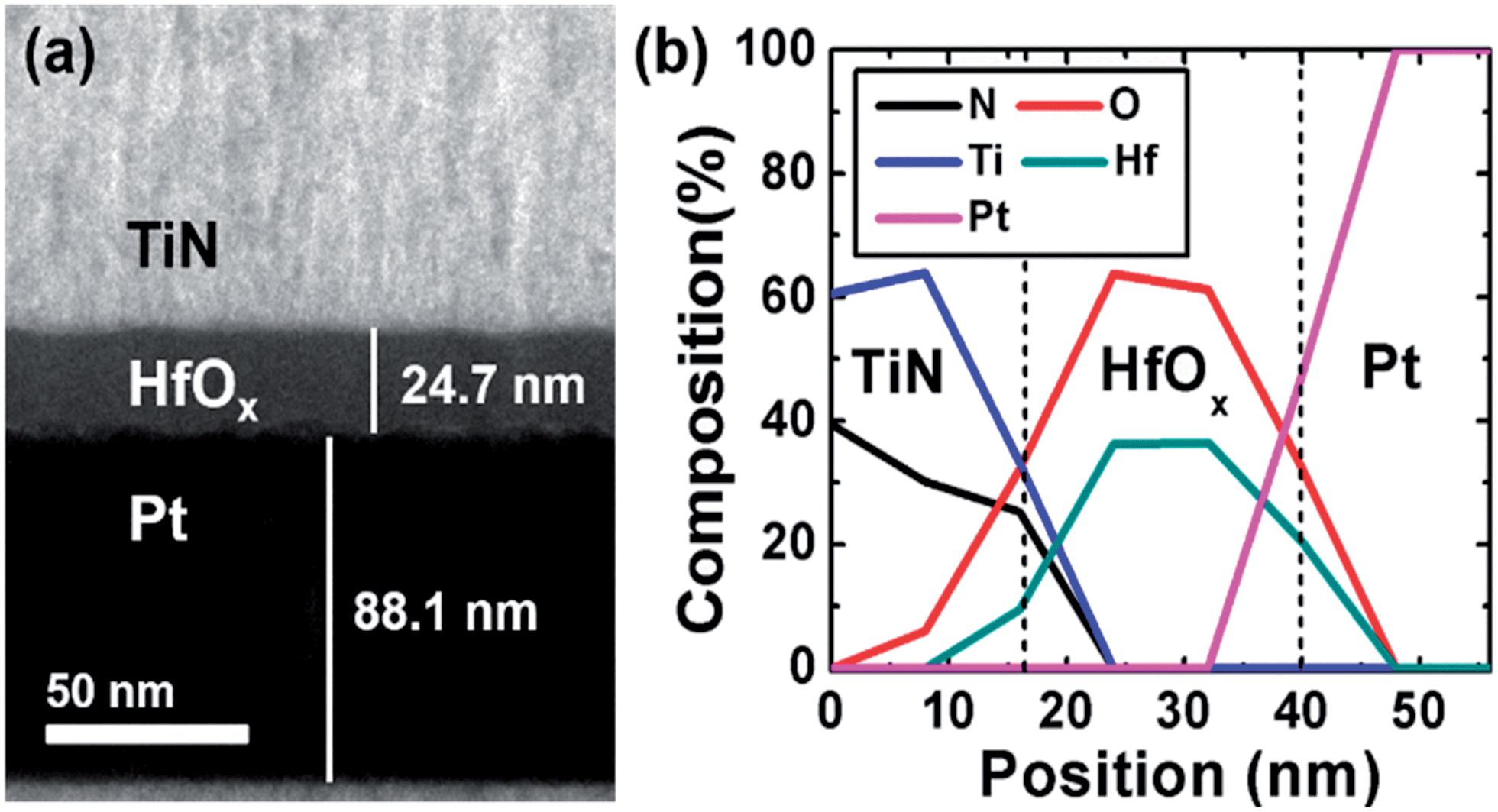 | ||
| Fig. 1 (a) Cross-sectional TEM image of the fabricated TiN/HfOx/Pt ReRAM device. (b) Elemental compositions throughout the device obtained by energy-dispersive X-ray spectroscopy (EDX). | ||
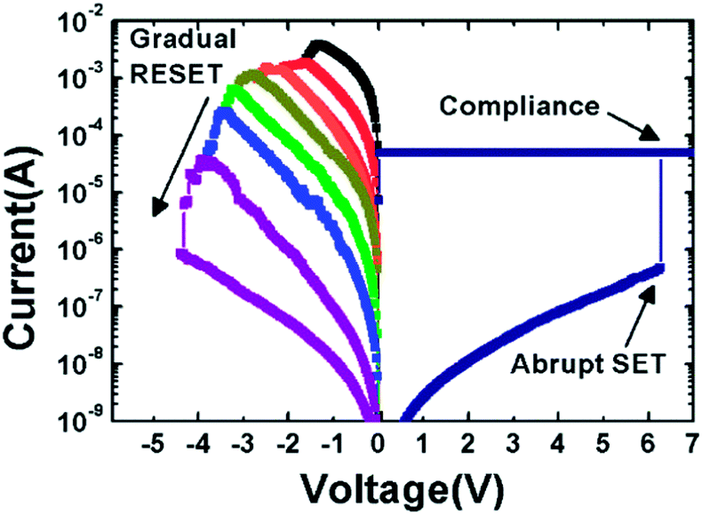 | ||
| Fig. 2 DC sweep characteristics of the fabricated ReRAM device. 8 resistance levels are achieved with a maximum ON/OFF ratio of ∼106. | ||
Fig. 3(a) shows the resistance distributions obtained in 100 consecutive DC sweep cycles at different RESET voltages. At smaller voltages, the uniformity of the high resistance state (HRS) is well-controlled, with resistance levels clearly separated from each other. However, when higher RESET voltages are applied to reach deep HRSs, the variations are noticeably increased. Fig. 3(b) shows the retention data collected from 8 resistance states measured at 125 °C, which can be extrapolated to 10 years. These results confirm the 3 bit per cell capability of the fabricated devices.
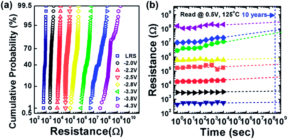 | ||
| Fig. 3 (a) Resistance distributions obtained from 100 consecutive DC sweep cycles at different RESET voltages. (b) Retention characteristics of 8 different resistance levels, measured up to 104 seconds at 125 °C. Retention can be extrapolated to 10 years. | ||
Compared to the DC sweep, pulse programming is a more desirable approach for practical applications due to high operation speed and energy efficiency. Multiple resistance levels can be achieved by varying either the widths or amplitudes of RESET pulses.22 However, these single-pulse schemes often result in cycle-to-cycle variations that are worse than the DC sweep, which reduces the margins between resistance levels and lowers the storage capacity. In the case of our 3 bit per cell ReRAM, controlling multiple levels by a single-pulse scheme becomes extremely challenging. Fig. 4(a) shows the relative standard deviations of 7 HRSs achieved by applying single pulses with various amplitudes. Compared to the DC sweep (Fig. 4(b)), most of the resistance states exhibit larger variations which cause severe overlapping between the adjacent levels. The only exception is the lowest HRS, which has very small variation due to reset failures. Varying pulse widths are not studied in this work because the required pulse width increases exponentially (which is six orders of magnitude), and the uniformity is unlikely to be improved compared to a varying pulse amplitude.22 The large variations of the single-pulse scheme can be partially attributed to the presence of only one rising edge, which causes the random atomic drift/diffusion to be ‘quenched’ in the device after the pulse. According to the recent studies on pulse rise-time of ReRAM,31 the switching voltages can be substantially affected by the rising edge of the pulses. Thus, applying a pulse-train operation scheme should not be viewed as an equivalent single pulse with the longer width of the pulse-train's cumulative time. Overall, the single-pulse operation scheme is not a favorable approach to control the filament evolution of this 3 bit per cell ReRAM due to the uncontrollable variation among the adjacent levels.
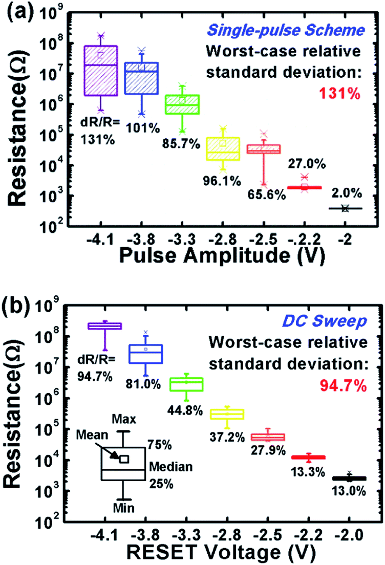 | ||
| Fig. 4 (a) Distributions of HRS resistances in 30 switching cycles obtained by the single-pulse scheme. (b) Distributions of HRS resistances in 100 DC sweep cycles. 7 different HRSs are studied to evaluate the MLC capability. | ||
On the other hand, pulse-train operation has been suggested to minimize the reset failures of ReRAM.32,33 It also emerges as a natural method to control analog synaptic devices for neuromorphic applications.24–27 In this study, the possibility of using a train of identical pulses to achieve multi-level switching with better uniformity is investigated. In this way, we hope to improve the control of the filament evolution by suppressing the stochasticity arising from sharp rising edges. Fig. 5 shows the variation of the resistances during the sequential applications of 100 identical pulses with various amplitudes. Three distinct regimes are observed in these characteristic curves: initially, the resistance changes slowly, then begins to rapidly increase at a certain point, and finally becomes saturated with some fluctuations around a certain value. Following the conventions of MOSFET, the three regimes can be denoted as the subthreshold region, linear region and saturation region. The subthreshold region could be responsible for RESET failures at low voltages,34 and it is generally eliminated at higher voltages. The linear region is where the majority of atomic migrations occurs, which in this case is controlled in a continuous manner. After entering the saturation region, the range of resistance fluctuation is comparable or even smaller than the cycle-to-cycle variations during the DC sweep. These pulse-trained characteristics, except for the initial random fluctuations, can be well reproduced by ReRAM compact modelling.35 The observations suggest that if the device reaches its saturation regime, the resistances should become more uniform and insusceptible to further identical stimuli.
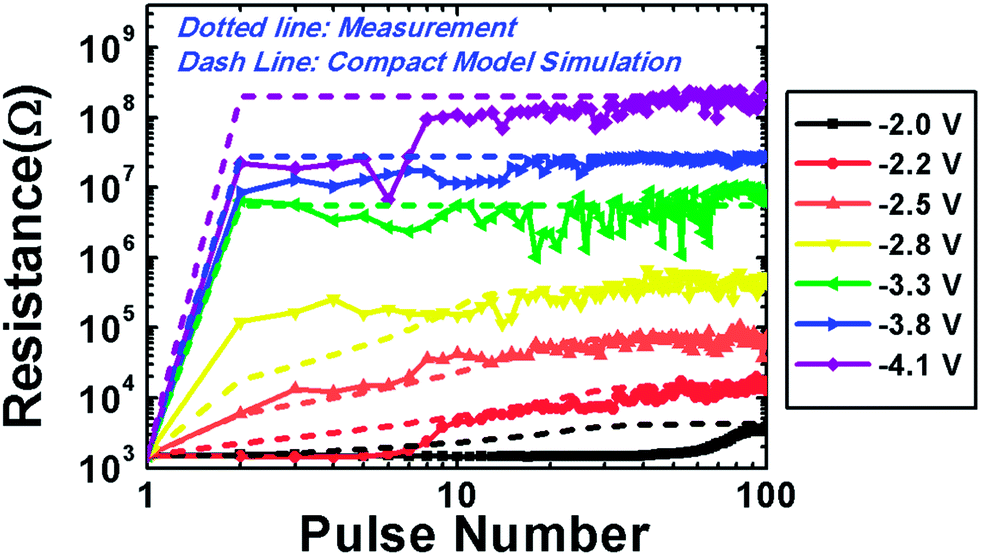 | ||
| Fig. 5 Double log plot of the resistance changes upon the applications of 100 identical pulses with different amplitudes. Both measurement data and compact-model simulation results are demonstrated. | ||
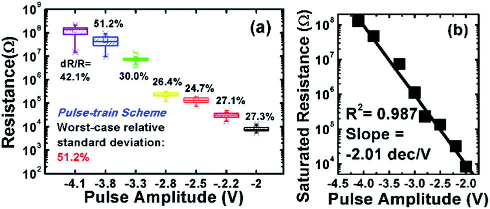
According to this observation, the pulse-train scheme using 100 identical pulses of 200 ns width is applied to program the fabricated HfO2 device to 7 different HRSs. Each of the resistance state is programmed for 30 switching cycles. As shown in Fig. 6(a), the new scheme significantly improves the variations compared to the single-pulse scheme. The relative standard deviation in the worst case is improved to 51%, which contributes to better separation of the resistance levels. Moreover, the mean saturated resistances are comparable to the corresponding HRS resistances from the DC sweep, and increase exponentially with the pulse amplitude (Fig. 6(b)).
 | ||
| Fig. 6 (a) Distributions of HRS resistances in 30 switching cycles obtained by the pulse-train scheme. (b) Relationship between the pulse amplitudes and the mean values of the HRS resistance by the pulse-train scheme. | ||
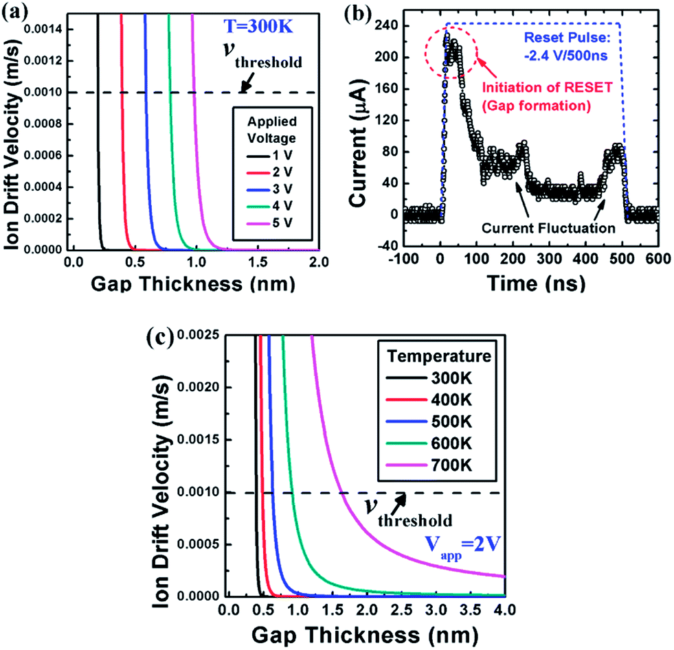
During the RESET process, it is widely accepted that the conductive filament(s) is (are) ruptured to form a tunnelling gap between the filament(s) and the electrode. According to the Wentzel–Kramers–Brillouin (WKB) approximation, the tunneling current across the gap is exponentially dependent on the gap thickness (tgap).36 The abovementioned results thus suggest the existence of a maximum gap thickness (tgap,max), which is linearly dependent on the RESET pulse amplitude. Fig. 7(a) further explains the formation of such a maximized gap by plotting the oxygen drift velocity as a function of the gap thickness. The vacancy migration probability is exponentially dependent on the applied electric field, which is reflected in the drift velocity of the oxygen atom:14,16
v = fa![[thin space (1/6-em)]](https://www.rsc.org/images/entities/char_2009.gif) exp(−Em/kT)sinh(qFa/2kT) exp(−Em/kT)sinh(qFa/2kT) | (1) |
 | ||
| Fig. 7 (a) Ion drift velocity in HfO2 ReRAM as a function of gap thickness, at a fixed temperature and various applied voltages. (b) Measured transient current of the HfO2 ReRAM device during a RESET pulse. (c) Ion drift velocity in HfO2 ReRAM as a function of the gap thickness, at a fixed applied voltage and various different temperatures. | ||
Next, the difference between a pulse train and a single pulse with the same equivalent duration is further discussed. Fig. 7(b) shows the transient current of a HfO2 ReRAM device during the RESET pulse. Beginning at the rising edge, the RESET process is not initiated until the current reaches the highest level. Then, the current drops quickly for about 100 ns before reaching the steady state with fluctuations. Before and after initiation, the progress of RESET is totally different even if the current levels are the same. This suggests that the initiation of RESET is a thermal-assisted event which can be connected with gap formation, and the first RESET pulse can be divided into two regimes. Before initiation, the filament is connected and the voltage drop is rather uniform across the entire film thickness. A significant amount of heat is needed to rupture the filament by ion diffusion at its weakest spot. This argument is supported by numerical simulations of transient thermal responses in the ON state,37 which confirms the rapid rise of the temperature as a complementary driving force during RESET. After initiation, the tunneling gap is formed and the voltage drop is concentrated to the gap. Now the reset process is field-driven and dominated by an ionic drift, without the need for a high temperature or current level.
The characteristics of pulse-train operation can be well explained within this picture. The subthreshold region corresponds to the condition before initiation of RESET. In the linear region, the gap thickness is gradually expanded until the maximum/saturation is reached. Now according to previous simulations,37,38 only the pulses before gap formation can create high temperatures in the filament. The rapid temperature rise suggests slow heat dissipation in the filament, which causes elevated temperatures in the first RESET pulse. According to eqn (1), this results in large variations of the ion migration speed (Fig. 7(c)) and hence larger resistance variations. After the first pulse, the stochasticity induced by the elevated temperatures is quenched in the device. On the other hand, the pulse-train scheme allows correction of this stochasticity with subsequent pulses which result in low temperatures. Since the process is now field-driven, the resistance monotonically increases and is strictly limited by the maximum gap thickness, thereby providing better uniformity.
Fig. 8 summarizes the proposed filament evolution during the course of pulse-train programming. The different natures of the pulse-trained characteristics happen to satisfy the requirements of different applications: the saturation region is desired for precise MLC control, while the linear region can be utilized in both MLC switching and neuromorphic computing. From Fig. 5, 10 identical pulses are sufficient to bring the device into saturation for most resistance levels, which suggests that the pulse amplitude is an efficient knob for exponential resistance modulation. On the other hand, linear resistance modulation is often desired for multi-level digital memory, which demands a lower dynamic range of the sense amplifiers. In this case, a proper combination of the varying pulse number and amplitude can help to optimize the device performance. Finally, we wish to point out that the idea of pulse-train operation discussed here is not limited to ReRAM, but also applicable to the fine control of other nanostructures such as metal-ion-based atomic switches and magnetic domain wall motion.39,40
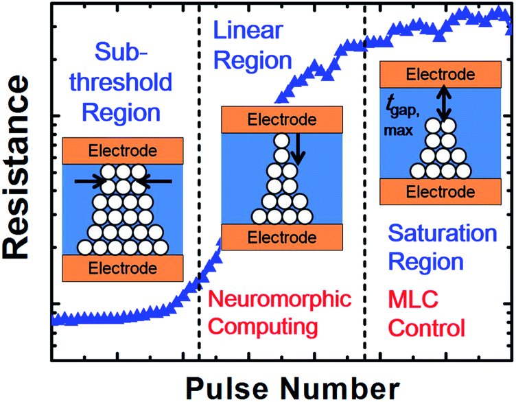 | ||
| Fig. 8 Schematic of the pulse-train characteristics of ReRAM, divided into three regions. The corresponding physical processes and applications are outlined and discussed in the framework of filamentary resistive switching. | ||
Conclusions
In summary, we systematically investigated the pulse-train operation scheme for reliable and uniform multi-level control of conductive-filament evolution in ReRAM. By applying electrical pulse-train to a 3 bit per cell HfO2 device, the relative standard deviation of resistance levels is improved up to 80% compared to the single-pulse scheme. Furthermore, the observed exponential relationship between the saturated resistance and the pulse amplitude is consistent with the gap-formation model of the filament rupture process.Experimental
The bottom electrode of Pt (∼90 nm) is first deposited by e-beam evaporation on Si wafer with a 2 nm Ti adhesion layer. Then, HfOx and TiN (∼200 nm) were deposited by reactive sputtering at room temperature, followed by a lift-off process to form ReRAM cells of 100 × 100 μm2 area. The device characteristics are measured using a Keithley 4200-SCS semiconductor analyzer with the pulsed I–V module. The length of the applied pulses is 200 ns, with a rise/fall time of 20 ns.Acknowledgements
This work was supported in part by the member companies of the Stanford Non-Volatile Memory Technology Research Initiative (NMTRI). H.-Y. Chen is additionally supported by the Intel Fellowship and the Taiwanese Government Scholarship to Study Aboard (GSSA). S.-C. Wu is additionally supported by the Taiwanese Government Graduate Student Study Abroad Program (GSSAP). Z. Jiang is additionally supported by the M. Stanley Rundel Fellowship Fund at Stanford University. S. Yu is additionally supported by the Stanford Graduate Fellowship.Notes and references
- H.-S. P. Wong, H.-Y. Lee, S. Yu, Y.-S. Chen, Y. Wu, P.-S. Chen, B. Lee, F. T. Chen and M.-J. Tsai, Proc. IEEE, 2012, 100, 1951 CrossRef CAS.
- R. Waser, R. Dittmann, G. Staikov and K. Szot, Adv. Mater., 2009, 21, 2632 CrossRef CAS.
- H. Akinaga and H. Shima, Proc. IEEE, 2010, 98, 2237 CrossRef CAS.
- Y. M. Kim and J. S. Lee, J. Appl. Phys., 2008, 104, 114115 CrossRef PubMed.
- H. Y. Lee, P. S. Chen, T. Y. Wu, Y. S. Chen, C. C. Wang, P. J. Tzeng, C. H. Lin, F. Chen, C. H. Lien and M.-J. Tsai, IEEE Int. Electron Devices Meet., Tech. Dig., 54th, 2008, 297 CAS.
- B. Govoreanu, G. S. Kar, Y. Chen, V. Paraschiv, S. Kubicek, A. Fantini, I. P. Radu, L. Goux, S. Clima, R. Degraeve, N. Jossart, O. Richard, T. Vandeweyer, K. Seo, P. Hendrickx, G. Pourtois, H. Bender, L. Altimime, D. J. Wouters, J. A. Kittl and M. Jurczak, IEEE Int. Electron Devices Meet., Tech. Dig., 57th, 2011, 31.6 Search PubMed.
- J. F. Gibbons and W. E. Beadle, Solid-State Electron., 1964, 7, 785 CrossRef CAS.
- U. Russo, D. Ielmini, C. Cagli and A. L. Lacaita, IEEE Trans. Electron Devices, 2009, 56, 186 CrossRef CAS.
- K. M. Kim, D. S. Jeong and C. S. Hwang, Nanotechnology, 2011, 22, 254002 CrossRef PubMed.
- J. Y. Son and Y.-H. Shin, Appl. Phys. Lett., 2008, 92, 222106 CrossRef PubMed.
- D.-H. Kwon, K. M. Kim, J. H. Jang, J. M. Jeon, M. H. Lee, G. H. Kim, X.-S. Li, G.-S. Park, B. Lee, S. Han, M. Kim and C. S. Hwang, Nat. Nanotechnol., 2010, 5, 148 CrossRef CAS PubMed.
- G. Bersuker, D. C. Gilmer, D. Veksler, P. Kirsch, L. Vandelli, A. Padovani, L. Larcher, K. McKenna, A. Shluger, V. Iglesias, M. Porti and M. Nafría, J. Appl. Phys., 2011, 110, 124518 CrossRef PubMed.
- P. Calka, E. Martinez, V. Delaye, D. Lafond, G. Audoit, D. Mariolle, N. Chevalier, H. Grampeix, C. Cagli, V. Jousseaume and C. Guedj, Nanotechnology, 2013, 24, 085706 CrossRef CAS PubMed.
- X. Guan, S. Yu and H.-S. P. Wong, IEEE Trans. Electron Devices, 2012, 59, 1172 CrossRef.
- L. Vandelli, A. Padovani, L. Larcher, G. Broglia, G. Ori, M. Montorsi, G. Bersuker and P. Pavan, IEEE Int. Electron Devices Meet., Tech. Dig., 57th, 2011, 17.5 Search PubMed.
- D. Ielmini, IEEE Trans. Electron Devices, 2011, 58, 4309 CrossRef CAS.
- X. Guan, S. Yu and H.-S. P. Wong, IEEE Trans. Electron Devices, 2012, 59, 1183 CrossRef.
- B. Chen, B. Gao, S. W. Sheng, L. F. Liu, X. Y. Liu, Y. S. Chen, Y. Wang, R. Q. Han, B. Yu and J. F. Kang, IEEE Electron Device Lett., 2011, 32, 282 CrossRef CAS.
- M.-J. Lee, S. Han, S. H. Jeon, B. H. Park, B. S. Kang, S.-E. Ahn, K. H. Kim, C. B. Lee, C. J. Kim, I.-K. Yoo, D. H. Seo, X.-S. Li, J.-B. Park, J.-H. Lee and Y. Park, Nano Lett., 2009, 9, 1476 CrossRef CAS PubMed.
- W. C. Chien, Y. C. Chen, K. P. Chang, E. K. Lai, Y. D. Yao, P. Lin, J. Gong, S. C. Cai, S. H. Hsieh, C. F. Chen, K. Y. Hsieh, R. Liu, and C.-Y. Lu, IEEE International Memory Workshop (IMW), 2009 Search PubMed.
- M. Terai, Y. Sakotsubo, S. Kotsuji and H. Hada, IEEE Electron Device Lett., 2010, 31, 204 CrossRef CAS.
- S. Yu, Y. Wu and H.-S. P. Wong, Appl. Phys. Lett., 2011, 98, 103514 CrossRef PubMed.
- S. R. Lee, Y.-B. Kim, M. Chang, K. M. Kim, C. B. Lee, J. H. Hur, G.-S. Park, D. Lee, M.-J. Lee, C. J. Kim, U.-I. Chung, I.-K. Yoo and K. Kim, IEEE Symp. VLSI Tech. Dig., 2012, p. 71 Search PubMed.
- S. Yu, B. Gao, Z. Fang, H. Y. Yu, J. F. Kang and H.-S. P. Wong, Adv. Mater., 2013, 25, 1774 CrossRef CAS PubMed.
- D. Kuzum, S. Yu and H.-S. P. Wong, Nanotechnology, 2013, 24, 382001 CrossRef PubMed.
- S. H. Jo, T. Chang, I. Ebong, B. Bhavitavya, P. Mazumder and W. Lu, Nano Lett., 2010, 10, 1297 CrossRef CAS PubMed.
- S. Park, J. Noh, M.-I. Choo, A. M. Sheri, M. Chang, Y.-B. Kim, C. J. Kim, M. Jeon, B.-G. Lee, B. H. Lee and H. Hwang, Nanotechnology, 2013, 24, 384009 CrossRef PubMed.
- H. Y. Lee, Y. S. Chen, P. S. Chen, P. Y. Gu, Y. Y. Hsu, S. M. Wang, W. H. Liu, C. H. Tsai, S. S. Sheu, P. C. Chiang, W. P. Lin, C. H. Lin, W. S. Chen, F. T. Chen, C. H. Lien and M.-J. Tsai, IEEE Int. Electron Devices Meet., Tech. Dig., 57th, 2011, 19.7 Search PubMed.
- F. Alibart, L. Gao, B. D. Hoskins and D. B. Strukov, Nanotechnology, 2012, 23, 075201 CrossRef PubMed.
- C. Xu, D. Niu, N. Muralimanohar, N. P. Jouppi and Y. Xie, Proceedings of the 50th Annual Design Automation Conference. ACM, 2013 Search PubMed.
- R. Liu, H.-Y. Chen, H. Li, P. Huang, L. Zhao, Z. Chen, F. Zhang, B. Chen, L. Liu, X. Liu, B. Gao, S. Yu, Y. Nishi, H.-S. P. Wong and J. Kang, International Symposium on VLSI Technology, Systems and Applications (VLSI-TSA), 2014 Search PubMed.
- K. Higuchi, T. O. Iwasaki and K. Takeuchil, IEEE International Memory Workshop (IMW), 2012 Search PubMed.
- K. Yoo, B. S. Kang, Y. D. Park, M. J. Lee and Y. Park, Appl. Phys. Lett., 2008, 92, 202112 CrossRef PubMed.
- Y. Y. Chen, R. Degraeve, S. Clima, B. Govoreanu, L. Goux, A. Fantini, G. S. Kar, G. Pourtois, G. Groeseneken, D. J. Wouters and M. Jurczak, IEEE Int. Electron Devices Meet., Tech. Dig., 58th, 2012, 20.3 Search PubMed.
- X. Guan, S. Yu and H.-S. P. Wong, IEEE Electron Device Lett., 2012, 33, 1405 CrossRef CAS.
- S. Yu, X. Guan and H.-S. P. Wong, Appl. Phys. Lett., 2011, 99, 063507 CrossRef PubMed.
- B. Govoreanu, S. Clima, I. P. Radu, Y.-Y. Chen, D. J. Wouters and M. Jurczak, IEEE Trans. Electron Devices, 2013, 60, 2471 CrossRef CAS.
- U. Russo, D. Ielmini, C. Cagli and A. L. Lacaita, IEEE Trans. Electron Devices, 2009, 56, 193 CrossRef CAS.
- K. Terabe, T. Hasegawa, T. Nakayama and M. Aono, Nature, 2005, 433, 47 CrossRef CAS PubMed.
- L. Thomas, M. Hayashi, X. Jiang, R. Moriya, C. Rettner and S. Parkin, Science, 2007, 315, 1553 CrossRef CAS PubMed.
Footnote |
| † Electronic supplementary information (ESI) available. See DOI: 10.1039/c4nr00500g |
| This journal is © The Royal Society of Chemistry 2014 |