 Open Access Article
 This Open Access Article is licensed under a
 Creative Commons Attribution 3.0 Unported Licence
Graphene nanoribbon blends with P3HT for organic electronics†
Mirella
El Gemayel
a,
Akimitsu
Narita
b,
Lukas F.
Dössel
b,
Ravi S.
Sundaram
c,
Adam
Kiersnowski
bd,
Wojciech
Pisula
b,
Michael Ryan
Hansen
be,
Andrea C.
Ferrari
c,
Emanuele
Orgiu
a,
Xinliang
Feng
*b,
Klaus
Müllen
*b and
Paolo
Samorì
*a
aNanochemistry Laboratory, ISIS & icFRC, Université de Strasbourg & CNRS, 8 allée Gaspard Monge, 67000 Strasbourg, France. E-mail: samori@unistra.fr
bMax-Planck Institute for Polymer Research, Ackermannweg 10, 55124 Mainz, Germany. E-mail: muellen@mpip-mainz.mpg.de; feng@mpip-mainz.mpg.de
cCambridge Graphene Center, Department of Engineering, Cambridge University, 9 JJ Thomson Avenue, Cambridge CB3 OFA, UK
dPolymer Engineering and Technology Division Wroclaw University of Technology Wybrzeze Wyspianskiego 27, 50-370 Wroclaw, Poland
eInterdisciplinary Nanoscience Center (iNANO) and Department of Chemistry, Aarhus University, Gustav Wieds Vej 14, DK-8000 Aarhus C, Denmark
First published on 21st February 2014
Abstract
In organic field-effect transistors (OFETs) the electrical characteristics of polymeric semiconducting materials suffer from the presence of structural/morphological defects and grain boundaries as well as amorphous domains within the film, hindering an efficient transport of charges. To improve the percolation of charges we blend a regioregular poly(3-hexylthiophene) (P3HT) with newly designed N = 18 armchair graphene nanoribbons (GNRs). The latter, prepared by a bottom-up solution synthesis, are expected to form solid aggregates which cannot be easily interfaced with metallic electrodes, limiting charge injection at metal–semiconductor interfaces, and are characterized by a finite size, thus by grain boundaries, which negatively affect the charge transport within the film. Both P3HT and GNRs are soluble/dispersible in organic solvents, enabling the use of a single step co-deposition process. The resulting OFETs show a three-fold increase in the charge carrier mobilities in blend films, when compared to pure P3HT devices. This behavior can be ascribed to GNRs, and aggregates thereof, facilitating the transport of the charges within the conduction channel by connecting the domains of the semiconductor film. The electronic characteristics of the devices such as the Ion/Ioff ratio are not affected by the addition of GNRs at different loads. Studies of the electrical characteristics under illumination for potential use of our blend films as organic phototransistors (OPTs) reveal a tunable photoresponse. Therefore, our strategy offers a new method towards the enhancement of the performance of OFETs, and holds potential for technological applications in (opto)electronics.
Introduction
Over the past few years, a great effort has been devoted to the development of new organic semiconducting materials, combining solution processability, stability under ambient conditions, and high charge carrier mobility1–10 for applications in organic electronics and particularly in organic field-effect transistors (OFETs). OFETs can be fabricated by using either small molecules or polymeric semiconductors as electroactive layers. In the latter case, despite the fact that polydisperse molecules can form extended networks for efficient percolation of charges, due to their polycrystalline nature the obtained material is characterized by the presence of structural and morphological defects, grain boundaries and amorphous domains hampering efficient charge transport.11 To circumvent this problem, polymeric semiconductors have been blended with either small molecules or other (semi)conducting systems.11–19 By blending different components new functions can be conferred to the material and to the device,20 benefiting the properties brought about by each component and exceeding its individual performance. Such an effect varies with the degree of phase segregation between the different components in the blend. Amongst polymeric semiconductors, regioregular poly(3-hexylthiophene) – P3HT is a prototypical system for solution processed OFETs.21–25 The performance of P3HT based OFETs has been improved by co-deposition with graphene, revealing an over 20 times increase in charge carrier mobilities when compared to the pure P3HT.26 This enhanced electrical characteristic can be ascribed to the beneficial role of graphene, which builds preferential paths for charge transport, therefore increasing the overall hole mobility,27 similar to previous findings in OFETs based on carbon nanotubes with P3HT;28,29 however, this was accompanied by a decrease of the on–off current ratio (Ion/Ioff).Due to the fact that graphene has zero band-gap,30 with high charge carrier mobilities,31 it cannot be used as an electroactive component to be incorporated in the channel of a regular OFET. Significant effort was devoted to opening a band gap in graphene.32 One approach was to confine the two dimensional (2d) sheet of graphene creating graphene nanoribbons (GNRs).33 Fabrication of GNRs has been predominantly carried out by top-down methods, such as lithographic patterning of graphene sheets,34–36 longitudinal unzipping of carbon nanotubes,37–39 and chemical extraction from exfoliated graphite.40 However, these methods lead to the production of GNRs exhibiting a broad (10–100 nm) width distribution37–39 as well as defective edge structures, resulting in GNRs with non-uniform electronic properties, e.g. band gap and ionization potential. In addition, top-down methods for the production of GNRs typically suffer from very low yield, hindering practical applications of the GNRs.37 In contrast, a bottom-up synthetic approach based on solution-mediated41–44 and surface-assisted45 cyclodehydrogenation46,47 of tailor-made polyphenylene precursors has been developed, enabling the fabrication of a variety of uniform and structurally defined GNRs with a lateral width of ca. 1–2 nm, which possess large and defined band gaps (1.1–1.7 eV).42,45 By using the solution-mediated method it is possible to produce GNRs in a large scale with a relatively high yield, as well as to render the GNRs dispersible in organic solvents by installing solubilizing groups at the peripheral positions.41,42,44 It was calculated that the absolute value of the valence band, which is related to the ionization potential, decreases as the GNRs extend laterally.48 We have recently reported laterally extended GNRs with a width of 1.54–1.98 nm, but the absolute value of the valence band of these GNRs was estimated to be still higher than that of P3HT, hindering the use of these GNRs for blending with P3HT.42,48 Further, the edges of these GNRs contain a cove-type structure, and the fabrication of broad (∼2 nm) and fully armchair edged GNRs has remained a challenge.
In this work we present the solution synthesis of N = 18 armchair GNR 1 (Fig. 1a) with a width of ∼2.1 nm, based on molecular modeling, surpassing all the GNRs hitherto fabricated by the bottom-up synthesis. GNR 1 features an ionization energy (IE) close to that of P3HT, making it the ideal candidate for the present study, in particular to avoid traps and energy barriers within the bi-component film. The edge decoration with long alkyl chains makes GNR 1 dispersible in common organic solvents such as tetrahydrofuran (THF), chlorobenzene and ortho-dichlorobenzene (ODCB), enabling its integration into organic electronic devices.
 | ||
| Fig. 1 Chemical formulae of (a) GNR 1 and (b) poly(3-hexylthiophene) (P3HT). | ||
GNR 1 has been blended with regioregular poly(3-hexylthiophene) – P3HT (Fig. 1b). We note that the alkyl chains exposed at the peripheral positions of GNR 1 provide a good affinity for P3HT, as an attempt to minimize the occurrence of macroscopic phase segregation. This is particularly important because of the problems associated with the propensity of GNRs to form microscopic crystals that cannot be easily interfaced with metallic electrodes, therefore limiting charge injection at the metal–(semi)conductor interface. Moreover, these microcrystals are alternated by domain boundaries hampering the charge transport within the film. The effect of the GNRs at different concentrations (in the blend) on the device performance in the dark, such as the field-effect mobility and Ion/Ioff, has been investigated. The influence of illumination with monochromatic light on the electrical characteristics of the device has been studied aiming at exploring the potential use of this blend as an active layer in hybrid organic phototransistors (OPTs).
Results and discussion
Synthesis of GNR 1
Scheme 1 portrays the synthetic route towards GNR 1. Our recent study has shown that the AA-type Yamamoto polymerization from one single monomer42,49,50 is more efficient for the synthesis of high-molecular-weight polyphenylene precursors than the A2B2-type Suzuki polymerization that requires heterogeneous reaction conditions involving two different monomers.41,44,51AB-type Diels–Alder polymerization has proved to be superior to transition-metal-catalyzed couplings for synthesizing long (>100 nm) GNRs, but the width of GNRs is only ∼1 nm.52 In order to build up laterally extended, N = 18 armchair GNR 1 by employing Yamamoto polymerization, the dihalogenated monomer 5 was designed (Scheme 1). Unlike previously reported monomers that lead to GNRs with the same widths as the monomers,42–44,52 the polymerization of monomer 5 with an o-terphenyl-based backbone structure would yield laterally expanded polyphenylene precursor 6 with twice the width of the monomer. Precursor 6 would be “graphitized” and “planarized” into GNR 1 with high structural definition albeit slight structural isomerization at the ends of the GNRs (Scheme S2†). For the synthesis of monomer 5, cyclopentadienone 4 was first prepared by Knoevenagel condensation of di(3-biphenylyl)acetone (2) and 4,4′-dichlorobenzil (3), and then subjected to Diels–Alder reaction with bis(4-dodecylphenyl)acetylene to yield monomer 5 (Scheme 1). Subsequently, Yamamoto polycondensation of monomer 5 was performed by employing a standard protocol,42,49,50 followed by fractionation using recycling preparative size exclusion chromatography (SEC) to provide precursor 6. Weight-average molecular weight (Mw) and polydispersity index (PDI) of precursor 6 were estimated by SEC analysis to be ca. 10![[thin space (1/6-em)]](https://www.rsc.org/images/entities/char_2009.gif) 000 g mol−1 and 1.4, respectively, against polystyrene (PS) standards (Fig. 2a). When the poly(p-phenylene) (PPP) standard calibration was applied, an Mw of ca. 7300 g mol−1 and a PDI of 1.3 were obtained. Considering the kinked and flexible polyphenylene backbone structure of precursor 6 with long alkyl chains at the peripheral positions, the actual Mw of 6 presumably lies between these two values, i.e. 7300–10000 g mol−1. Matrix-assisted laser desorption/ionization time-of-flight (MALDI-TOF) mass spectrometry (MS) analysis of precursor 6 showed a regular mass pattern extending up to ∼20000 g mol−1, which corresponds to the molecular weight of ∼20 repeating units (Fig. 2b). Based on this result, the longitudinal length of the resulting GNR 1 could be estimated to be up to ca. 10 nm. It should be noted however that this is most probably not the highest value, taking into account the limitation of MALDI-TOF MS for the analysis of large polymers with broad molecular weight distribution.41,42,53
000 g mol−1 and 1.4, respectively, against polystyrene (PS) standards (Fig. 2a). When the poly(p-phenylene) (PPP) standard calibration was applied, an Mw of ca. 7300 g mol−1 and a PDI of 1.3 were obtained. Considering the kinked and flexible polyphenylene backbone structure of precursor 6 with long alkyl chains at the peripheral positions, the actual Mw of 6 presumably lies between these two values, i.e. 7300–10000 g mol−1. Matrix-assisted laser desorption/ionization time-of-flight (MALDI-TOF) mass spectrometry (MS) analysis of precursor 6 showed a regular mass pattern extending up to ∼20000 g mol−1, which corresponds to the molecular weight of ∼20 repeating units (Fig. 2b). Based on this result, the longitudinal length of the resulting GNR 1 could be estimated to be up to ca. 10 nm. It should be noted however that this is most probably not the highest value, taking into account the limitation of MALDI-TOF MS for the analysis of large polymers with broad molecular weight distribution.41,42,53
 | ||
| Scheme 1 Synthesis route to GNR 1. Reagents and conditions: (a) tetrabutylammonium hydroxide, tBuOH, 80 °C, 77%; (b) bis(4-dodecylphenyl)acetylene, Ph2O, 230 °C, μW, 300 W, 56%; (c) bis(cycloocta-(1,5)-diene)nickel(0), cycloocta-(1,5)-diene, 2,2′-bipyridine, toluene/DMF, 80 °C, 86% (before fractionation); (d) FeCl3, CH2Cl2/CH3NO2, rt, 98%. | ||
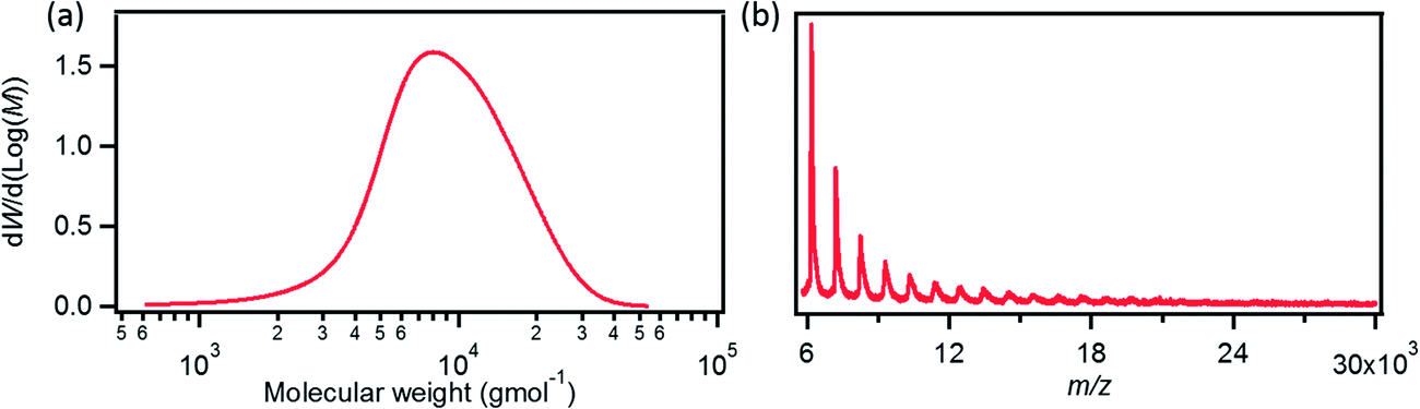 | ||
| Fig. 2 (a) Molecular weight distribution of polyphenylene precursor 6 (SEC analysis, eluent: THF, polystyrene standard). (b) Linear-mode MALDI-TOF MS spectrum of polyphenylene precursor 6. | ||
The intramolecular cyclodehydrogenation of precursor 6 was carried out by using an established method, applying iron(III) chloride as the Lewis acid and oxidant in a mixture of dichloromethane and nitromethane.41–44,47 MALDI-TOF MS analysis of GNR 1 in linear mode displayed a regular mass pattern similar to that of precursor 6 (Fig. S4 in the ESI†). Although the peaks were strongly broadened, the interval was roughly ∼1000 g mol−1, corresponding to the molecular weight of one repeating unit of GNR 1, i.e. 991 g mol−1. More accurate analysis as well as detection of mass exceeding 15000 g mol−1 was not possible most probably due to the strong self-association tendency of larger GNRs and fragmentations at higher laser powers.42,53
Comparison of Fourier transform infrared (FTIR) spectra of precursor 6 and GNR 1 displayed disappearance of the band from the rotation of free phenyl rings at 4052 cm−1, as well as strong attenuation of the signal triad from aromatic C–H stretching vibrations at 3029, 3054, and 3084 cm−1, after the cyclodehydrogenation (Fig. 3).41,42,54 Further, out-of-plane (opla) C–H deformation bands in the fingerprint regions such as at 698, 841, and 897 cm−1 vanished, validating the disappearance of mono- and di-substituted benzene rings.54,55 These results indicated the high efficiency of the cyclodehydrogenation of precursor 6 leading to successful formation of GNR 1.
 | ||
| Fig. 3 Representative FTIR spectral regions of polyphenylene precursor 6 (red) and GNR 1 (blue). | ||
To further characterize the cyclodehydrogenation of precursor 6 into GNR 1, we have used liquid- and solid-state 1H NMR spectroscopy as summarized in Fig. 4. This analysis makes it possible to follow the structural changes before and after cyclodehydrogenation, since the 1H chemical shift (position and line width) is known to be a highly sensitive probe for non-covalent interactions.56–59 The 1H NMR spectra in Fig. 4a and b unambiguously reveal that precursor 6 possesses a semi-flexible/semi-rigid structure due to the fact that the overall 1H line width from the polyphenylene groups at ∼7.0 ppm is almost unchanged, when going from the liquid- to the solid-state NMR spectrum (Fig. 4a and b, respectively). After cyclodehydrogenation, the 1H magic-angle spinning (MAS) NMR spectrum of GNR 1 shown in Fig. 4c includes significantly broadened 1H resonances, where, in particular, those related to the aromatic signals are shifted to a higher frequency (or equivalently to lower field). The broad nature and shift of the aromatic 1H signals demonstrate that these are part of an extended π-conjugated system,60,61 and that GNR 1 behaves like a rigid solid, consistent with the formation of GNRs. Fig. 4d and e display the 2d 1H–1H double quantum-single quantum (DQ-SQ) NMR correlation experiments mapping out the spatial connectivities between the different 1H signals for precursor 6 and GNR 1.62,63 For precursor 6, the 2D 1H–1H DQ-SQ spectrum includes narrow 1H–1H correlation signals between polyphenylene groups as well as between the polyphenylene groups and the dodecyl side chains as one might expect for a flexible structure. However, after cyclodehydrogenation, GNR 1 shows a broad, stretched split ridge of 1H–1H correlation signals close to the spectrum diagonal in the range between ∼9 and 12 ppm (Fig. 4e), in addition to a clear, albeit broad, 1H–1H correlation between aromatic protons at ∼6–9 ppm and those of the dodecyl side chains. Based on these spectral differences we can make the assignment shown in Fig. 4f, where the high-frequency part is attributed to the protons at the end of GNR 1 (blue) and the lower-frequency part to the protons of the edge (red) in close spatial proximity to the dodecyl side chains. Note that the edge protons (red) of GNR 1 only show a small shift of ∼1–2 ppm to high frequency when compared to precursor 6, while a much larger shift of ∼2–5 ppm is observed for the end protons (blue). These differences illustrate that the bulk sample of GNR 1 is heterogeneously packed, shifting the 1H signals as a result of the different magnitudes for the aromatic ring currents of stacked GNRs.64,65
 | ||
| Fig. 4 Liquid- and solid-state 1H NMR spectra of (a) precursor 6 in CD2Cl2, and (b and c) solid samples of precursor 6 and GNR 1, respectively. The 2d 1H–1H DQ-SQ correlation spectra of (d) precursor 6 and (e) GNR 1 were recorded using two rotor periods of DQ recoupling. The 1H signals are assigned using the color code given in (f); all the aromatic signals of 6 are represented by the red color. The liquid-state spectrum in (a) was recorded at 7.05 T (300.13 MHz for 1H), while the solid-state NMR experiments in (b–e) were obtained at 16.45 T (700.21 MHz for 1H) using a MAS frequency of 59524 Hz. The asterisks in (a) mark the residual proton signals of CD2Cl2. The sharp signals in (c) represent residual solvent present in the sample. | ||
The successful conversion of precursor 6 into GNR 1 was further verified by investigation of a model monomer S4, for which the efficient cyclodehydrogenation was demonstrated by the combination of 1H NMR and MALDI-TOF MS analysis (see ESI†).
GNR 1 can be easily dispersed in common organic solvents such as THF, chlorobenzene, and ODCB by applying mild sonication to give brown dispersions. Such dispersions of GNR 1 with typical concentrations up to ∼1 mg mL−1 in ODCB are stable for at least one week without apparent precipitation. The UV-vis absorption spectrum of a dispersion of GNR 1 in ODCB shows an absorption maximum at 410 nm with the absorption edge at ∼800 nm, corresponding to an optical bandgap ∼1.6 eV (Fig. S5†). Subsequently, different volumes of such dispersion in ODCB are mixed with solutions of P3HT for the fabrication of GNR-P3HT blend films with various GNR loading ratios by co-deposition.
Electrical, structural and morphological characteristics in the dark
Ambient photoelectron spectroscopy (PS) measurements of the pristine GNR 1 dropcasted film indicate a HOMO level of 5.010 ± 0.063 eV, close to that of P3HT, i.e. 4.860 ± 0.015 eV. Thereby, this result makes GNR 1 an ideal candidate for our case study.Then we fabricated devices at various GNR loading ratios (0, 2, 5, 11 and 24 wt% with respect to P3HT), having different channel lengths (L) ranging from 60 μm to 120 μm. Fig. 5a displays transfer characteristics of a 120 μm channel length device with 24% GNRs with its output characteristics shown as the inset, the device exhibits a typical p-type behavior. The extracted hole mobility (from the saturation regime at VD = −60 V), threshold voltage (Vth) and Ion/Ioff is 2.8 × 10⁻² cm2 V−1 s−1, −8.9 V and ∼103 respectively. The same channel length device based on pristine P3HT was also studied (transfer and output characteristics are shown in Fig. S6 in the ESI†). The only parameter that exhibited a notable change is the field-effect mobility μ, which amounted to 7.3 × 10⁻³ cm2 V−1 s−1. This shows that the performance of the device is enhanced in the presence of GNRs. Such an improvement can be ascribed to (i) the percolation pathway for the charges provided by the GNRs, or (ii) the ionization energy of the 24% blend, as determined by ambient PS, is 4.790 ± 0.016 eV (i.e. lowered by 0.07 eV as compared to the pure P3HT 4.860 ± 0.015 eV), thus it better matches the work function of the Au electrodes (4.810 ± 0.020 eV) enabling a better charge injection. A comparison of the transfer characteristics (at VD = −60 V) of the devices with the same L = 120 μm at different concentrations of GNRs is shown in Fig. 5b. It reveals an increase in Id with increase in the relative amount of GNRs up to a factor of 3 when comparing the 24% blend with the pristine devices (0% blend). Such a trend is also evident in Fig. 5c which compares the output characteristics of the same blend devices at VG = 0 V (dashed line) and at VG = −60 V (solid line).
 | ||
| Fig. 5 (a) Transfer characteristics of bottom-gate bottom-contact devices (L = 120 μm) prepared by blending 24% of GNRs with P3HT (left axis in the log scale). The inset shows their output characteristics. (b) Transfer characteristics of bottom-gate bottom-contact devices (L = 120 μm) prepared by different blend percentages of GNRs with P3HT, and (c) their output characteristics (solid line at VG = −60 V and dashed line at VG = 0 V; the rest of data at VG = −20 V and −40 V have been omitted for clarity). (d) Variation of the field-effect mobility (left axis in the log scale) with the channel length (60, 80, 100 and 120 μm) at different blend percentages of GNRs with respect to P3HT. | ||
Fig. 5d (see also Fig. S7 in the ESI†) shows the high variation of hole field-effect mobility at different concentrations of GNRs and for devices with different L. In particular, at 2 and 5% loadings, the field-effect mobility is comparable to that of the devices with pristine P3HT. The mobility increased ∼1.7 times when the content of GNRs augments to 11%, and by a factor of 3 at 24% with respect to P3HT. The enhanced performance can be attributed to the above mentioned reasons, and mainly to the amount of GNRs that can facilitate the charge transport within the conduction channel, as observed in similar studies on the P3HT blend with graphene,26 or with functionalized carbon nanotubes.29 Enhanced performances were also observed for other p-type polymers printed on the top of a graphene layer inside the channel.66 In fact, it has been demonstrated that when P3HT is blended with another semiconductor, there is a critical concentration for the enhancement of the mobility.28,67 When comparing all the devices at different blend % and different L spanning from 60 μm to 120 μm, the average Vth was found to range between 2 and −5 V, and to be slightly higher (up to −8 V) for those with 24% of GNR 1. Significantly, the average Ion/Ioff ranged between 103 and 104, and appeared unaffected by the presence of GNRs (see Fig. S8 in the ESI†), unlike blends with graphene where the Ion/Ioff markedly decreases at higher concentrations.26 Electrical characterization was also performed on shorter channel lengths ranging from 2.5 μm to 20 μm, with the results being reported in Fig. S9 in the ESI.†
To gain further insight into the relation between electrical properties and structure within the blend films, Grazing Incidence X-ray Diffraction (GIXD) measurements were carried out on the spin-coated films. This reveals that the addition of GNR 1 strongly influences the order within P3HT films. In the pattern recorded for the monocomponent P3HT film (Fig. 6a) the h00 series, corresponding to the interchain distance measured in the plane of aromatic rings, is discernible up to the third diffraction order. Another characteristic peak, originating from the π–π stacking of P3HT, is visible on the equator, indicating that in the pure P3HT film the macromolecules adopt an edge-on orientation in the crystalline domains. The chain-to-chain distance (16.4 Å), the π-stacking distance (3.6 Å) as well as the approximated coherence length of the π–π stacking derived from GIXD data (∼70 Å; Fig. 6a and c) are typical for P3HT films.68–70 The addition of GNR to P3HT affects the arrangement of the crystalline structure of the polymer. The absence of characteristic equatorial reflections at qx,y ≈ 1.72 Å−1 related to the π-stacking reflection in XRD patterns of all the blends (Fig. 6b and d) indicates that even a small amount of GNRs, such as 2 wt%, hinders the formation of coherent π-stacks. Increasing amounts of GNRs cause also a gradual decrease in the integral intensity of the 100 reflection (at qz = 0.377 Å−1), providing evidence for a decrease in lamellar ordering of P3HT macromolecules, hence in the overall crystallinity of the polymer. Unfortunately, a strong diffuse scattering of X-rays on the GNRs overlaps with P3HT peaks, which does not permit a quantitative analysis of the polymer crystallinity. On the other hand, such a strong scattering suggests the existence of a large interface area between the GNRs and P3HT. Increasing the GNR content beyond 5 wt% causes almost complete disappearance of diffraction features from the crystalline fraction of P3HT, which indicates that at the higher content of GNRs no significant polymer crystals are formed. We suggest that the increase of the mobility in the blend can be attributed to the presence of GNRs and aggregates thereof, providing favorable pathways for the transport of charges counteracting the effect of decreased crystallinity in the P3HT domains upon addition of GNR.
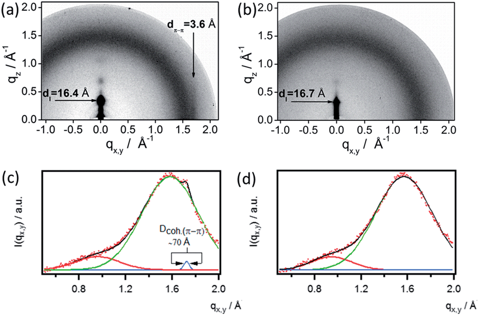 | ||
| Fig. 6 GIXD patterns of (a) P3HT film, (b) P3HT + 2 wt% GNR, and the corresponding horizontal integrations of (c) P3HT and (d) the blend. | ||
As the q-range in the GIXD experiments allowed studying structures with length scales up to a very few nanometers, in order to analyze the occurrence of possible phase separation on a length scale ranging from a few nanometers up to a few tens of micrometers we used atomic force microscopy in the tapping mode (TM-AFM). The pristine P3HT film from ODCB solution is homogeneous featuring fibrillar and grain-like structures on the tens of nanometers scale (Fig. 7a). At 24%, the P3HT/GNR films are inhomogeneous due to the aggregation of the GNRs as shown in Fig. 7b. These aggregates having a height ranging from 60 to 200 nm and a width spanning from 0.6 to 2 μm, were found to be randomly distributed within the polymer matrix. Their frequency of occurrence inside the channel, i.e. the number of aggregates located in the source–drain gap, was proportional to the concentration of GNRs; conversely, the aggregate size was found independent of the concentration (see Fig. S11 in the ESI†). This clarifies how the aggregates of GNRs, and not single GNRs, act as an “electronic bridge” between P3HT domains. Because of the high propensity of our GNRs to undergo aggregation when deposited on a solid surface, single component polycrystalline structures are obtained which are difficult to characterize, in line with observations on similar liquid phase-processable GNRs.52 It is indeed surprising to see the mild increase in field-effect mobility upon blending P3HT with the GNRs, given that it is known that a 2 nm wide GNR can exhibit a mobility around 100 cm2 V−1 s−1.71 Yet, a maximum field-effect mobility of 3.25 × 10⁻² cm2 V−1 s−1 was observed for a similar arm-chair GNR deposited from ODCB.72 Consequently, the reason for the limited increase in mobility is likely the simultaneous effect of decreased crystallinity with the P3HT film upon blending and charge scattering when encountering GNR aggregates.
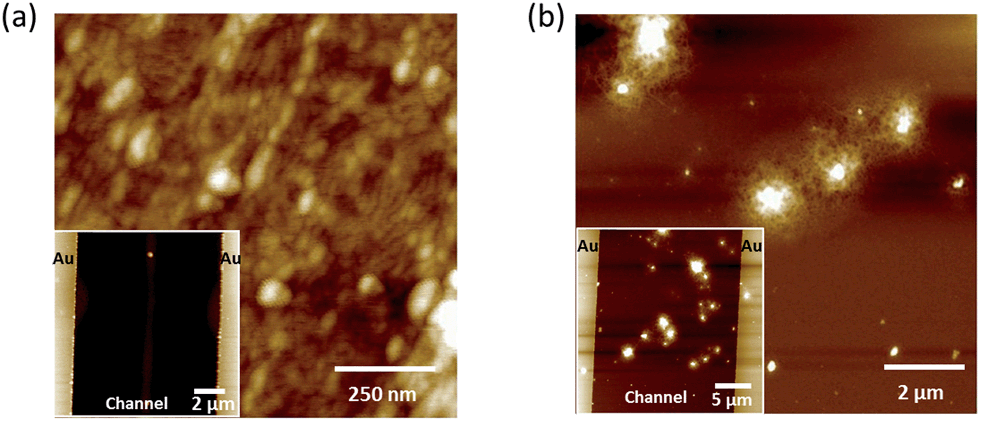 | ||
| Fig. 7 AFM images scanned inside the channel of films of: (a) pristine P3HT and (b) 24% GNR with P3HT. The insets show the scan at a larger scale. Z-scales: (a) 17 nm, (b) 75 nm, inset (a) 47 nm, inset (b) 92 nm. | ||
Electrical characteristics under illumination
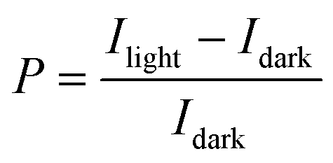
Measurements of the photoresponse under illumination at 605 nm and 560 nm were carried out to investigate both the potential application of these OFETs in optoelectronics and the influence of the GNRs on the photo-generated carriers. The two wavelengths were chosen because they correspond to two absorption peaks of the films (see Fig. S12 in the ESI†).The difference in output (ID–VD) and transfer (ID–VG) characteristics of a 0% and 24% OFET (L = 20 μm) in the dark and under illumination with monochromatic light (8.17 mW cm−2) at λ = 605 nm is illustrated in Fig. 8a–d. The electrical characteristics of a pristine P3HT based device, i.e. with 0% GNR in the blend, is shown in Fig. 8a and b. It displays an increase of the drain current in the ID–VD and ID–VG curves upon irradiation with monochromatic light as a result of the photogeneration of excitons that dissociate into free charge carriers which subsequently move towards the electrode under the influence of the electric field.73 The same was observed for the 24% blend. The only difference is that at VG = 20 V (VD = −60 V) the ratio of the photocurrent (Iph) (calculated by subtracting the dark current (Idark) from the current under light (Ilight, i.e. Iph = Ilight − Idark) to Idark is 251.71 for the device with 0% GNR (see Fig. 8b, e) whereas it was much lower (145.1) for the device with 24% blend (see Fig. 8d, e). This ratio, called photosensitivity P:
 | (1) |
 | (2) |
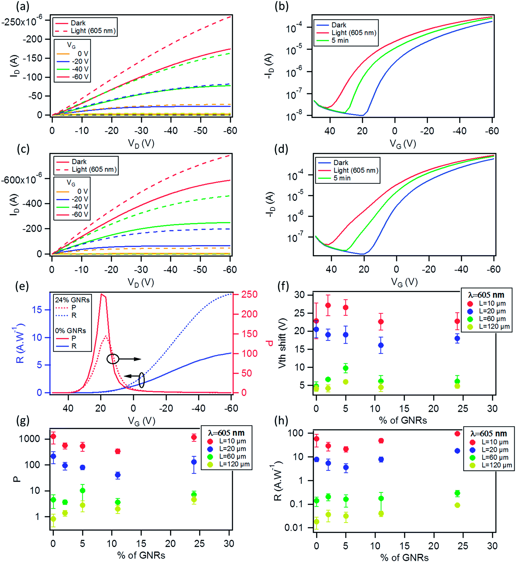 | ||
| Fig. 8 Comparison of (a) output and (b) transfer characteristics at VD = −60 V of pristine P3HT OFET; (c) output and (d) transfer characteristics at VD = −60 V of a device with 24% GNR blend with P3HT with the same channel length L = 20 μm measured in the dark and under monochromatic light (λ = 605 nm; 8.17 mW cm−2). (e) Variation of the responsivity R (blue curves) and photosensitivity P (red curves) with VG at VD = −60 V at λ = 605 nm for OFETs (L = 20 μm) with 0% (solid lines) and 24% blends of GNRs (dashed lines). (f) Threshold voltage shift under illumination with monochromatic light (λ = 605 nm; 8.17 mW cm−2) for 4 channel length (L = 10, 20, 60 and 120 μm) OFETs based on different blend percentages of GNRs with respect to P3HT. (g) Photosensivity (extracted at VG = 20 V), and (h) responsivity of these devices (extracted at VG = −60 V) both at VD = −60 V. The left axis is expressed in log-scale. | ||
The photoresponse was also measured at λ = 560 nm (9.44 mW cm−2), corresponding to the maximum absorption of the P3HT films, as shown in E12 in the ESI.† A much lower photoresponse is seen for L = 60 and 120 μm. By comparing the trend with the GNR% for the responsivity and photosensitivity to that at 605 nm, we find that R values are similar to those at 605 nm (Fig. S13a in the ESI†), whereas P values are slightly higher (Fig. S13b in the ESI†). Only a small increase in the photoresponse is observed by lowering the incident wavelength, which can be explained by (i) the greater energy of photons of λ = 560 nm when compared to λ = 605 nm and (ii) the small difference in the absorbance peaks at λ = 560 nm and 605 nm (Fig. S12 in the ESI†). For pristine P3HT devices, R and P for L = 10 μm are close to the ones reported in the literature.73,81 This suggests that the use of a monochromatic light source with a wavelength matching the peak of absorption of the semiconductor gives a higher photoresponse as compared to broadband illumination (see Fig. S13d in the ESI,† where the same device is tested under white light and monochromatic light at 605 and 560 nm). The field-effect mobility of the devices studied at both wavelengths remained relatively unaffected under illumination as compared to the one in the dark (see Fig. S13c in the ESI†). Furthermore, after 5 min of switching off the light, both devices at 0 and 24% did not regain their initial characteristics due to a photoinduced memory effect (Fig. 8b and d green plots). In view of this finding, we extended our study to the examination of this slow relaxation at different blend percentages as a function of the gate voltage (with VG = 0 V and without VG). Fig. 9a and b depict the relaxation mechanism of the photoinduced charges after illumination for 30 s for a 20 μm device with 0 and 24% blend respectively, measured at VD = −10 V. In both cases, the photoinduced current decreases slowly once the light source is switched off at t = 60 s (see Fig. 9a and b) and in the same manner regardless of the application (blue plots) or not (red plots) of a gate bias. The same result was observed for the other blend percentages. This decay was reported for regioregular P3HT82,83 and fitted to a stretched-exponential behavior (Kohlrausch's law) (grey curves in Fig. 9a and b):
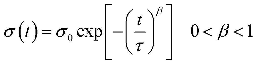 | (3) |
 | ||
| Fig. 9 (a) Relaxation characteristics of the photoinduced current after irradiation with monochromatic light (λ = 560 nm, 9.44 mW cm−2) (light on at 30 s, light off at 60 s) for a 0% blend, and (b) 24% GNR blend P3HT. The gray line is the fitting by Kohlrausch's law. Average variation of: (c) the exponent β (indicating the degree of the disorder of the material), and (d) the relaxation lifetime τ at different blend percentages (done on 5 to 6 devices for each blend %). | ||
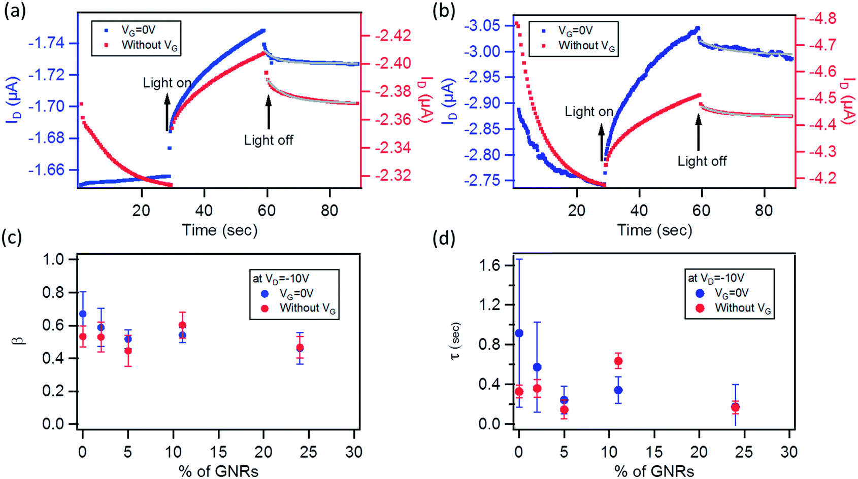
Photocurrent mapping
To gain more information about the local origin of the generated photoresponse and the role of the GNRs under illumination, we studied these devices using scanning photocurrent microscopy. This technique has been employed widely for the local photocurrent study of devices based on carbon nanotubes and graphene,84–88 and uses an optical microscope in combination with a multi-axis scanning stage for raster scanning the sample with respect to a laser beam focused on the device surface. We examined a device (L = 20 μm) with 24% GNRs blended with P3HT at VG = +30 V (in the off-state) and at zero source–drain bias under a ∼1 μm spot size laser (λ = 633 nm, power density <50 kW cm−2). The photocurrent image presented in Fig. 10 reveals uniform photocurrent response inside the channel indicating that the entire OFET channel is photoactive. However, a decrease in local photocurrent is observed in the areas where big aggregates of GNRs are present (see the black circle in Fig. 10a and the photocurrent profile in Fig. 10b). The difference could be explained by the fact that the photo-generated carriers in the aggregated region face higher impedance due to the potential barrier formed at the interface between the GNR aggregates (Eg GNR 1 = ∼1.6 eV) and P3HT (Eg P3HT = 1.9–2.0 eV) due the difference in their band gap (Fig. S5 in the ESI†). Therefore this barrier results in a lower photocurrent collected on local illumination in this region of the channel. However, this small difference does not strongly affect the overall performance of our phototransistors as demonstrated through measurements by illuminating the entire device area. | ||
| Fig. 10 (a) Zero drain bias photocurrent response for OFET with 24% GNR/P3HT and L = 20 μm in the off-state (VG = +30 V). The dashed white lines indicate the edges of the source and drain electrical contacts; the black circle indicates the observed aggregate of GNRs. (b) Variation of the photocurrent as a function of the position of the black dashed line in (a). | ||
Conclusion
In summary, we designed and synthesized N = 18 armchair graphene nanoribbons (GNR 1) with a good dispersibility in organic solvents and an ionization energy matching that of P3HT. GNR 1 was blended with P3HT in a single step co-deposition process. While monocomponent GNR films suffer from the presence of macroscopic crystals alternated by domain boundaries, thereby lacking in terms of extended percolation pathways for charge transport, we demonstrated that the addition of up to 24% of GNRs in a P3HT film enables improvement of percolation of charges in a P3HT transistor. In particular, it is possible to obtain a three-fold increase in the field-effect mobility in a P3HT device by adding 24% GNRs, without altering the other relevant electronic characteristics, such as the Ion/Ioff. This can be ascribed to the aggregates of GNRs acting as percolation paths for the charge carrier within the conduction channel by connecting the domains of the semiconductor film. Our P3HT – GNR blend, exhibiting an increased μ accompanied by an unaltered Ion/Ioff is a step forward towards the enhancement of the performance of OFETs. The transistor's photoresponse in GNR–P3HT binary mixtures depends on the quantity of each component in the blend as well as on the channel length. This may allow the use of these devices in (opto)electronics, where light can function as an additional control parameter.Experimental section
Materials
Poly(3-hexylthiophene) (P3HT) (Fig. 1b) (regioregularity >99%, Mw ∼ 50000 g mol−1, Sepiolid P-200 from BASF) was used as purchased. Other materials were purchased from Fluka, Aldrich, Acros, ABCR, Merck, and other commercial suppliers and used as received unless otherwise specified.
:10), and stirred overnight. The precipitates were collected by centrifugation and then repeatedly reprecipitated from THF solution in methanol to give the title compound as a white solid (780 mg, 86% yield). A part of the polymer was fractionated by preparative SEC (Bio-Beads S-X1 support, Bio-Rad Laboratories), and then further by recycling preparative SEC to obtain a polymer fraction with Mw = 1.0 × 10⁴ g mol−1, Mn = 7.2 × 10³ g mol−1, and PDI = 1.4 as well as a fraction with Mw = 1.2 × 10⁴ g mol−1, Mn = 9.3 × 10³ g mol−1, and PDI = 1.3 based on SEC analysis (UV detector, polystyrene standard): FTIR (powder): 4052, 3084, 3054, 3029, 2924, 2852, 1598, 1573, 1513, 1498, 1479, 1465, 1451, 1407, 1356, 1259, 1184, 1141, 1118, 1092, 1074, 1053, 1021, 1006, 965, 944, 897, 841, 807, 717, 698 cm−1.
Solid-state NMR analysis
All solid-state 1H NMR experiments were carried out on a Bruker AVANCE III 700 operating at a Larmor frequency of 700.21 MHz (16.45 T). The experiments employed a 1.3 mm H-X double-resonance magic-angle spinning (MAS) probe from Bruker, using a spinning frequency of 59524 Hz and a π/2-pulse length of 1.5 μs, corresponding to an rf-field strength of 167 kHz. The 2D 1H–1H double quantum-single quantum (DQ-SQ) correlation experiments were carried out using the compensated Back-to-Back (BaBa) dipolar recoupling sequence for both excitation and reconversion of DQ coherences followed by a z-filter, set to one rotor period, prior to a final π/2 pulse for creating transverse observable magnetization.62,63 A phase cycling scheme of 16 steps, a recycle delay of 2 s, and 16 scans per rotor-synchronized t1 increment were used. Prior to all experiments the magic angle was checked with KBr.911H chemical shifts are reported relative to TMS using solid adamantane as an external ref. 92 The 2D 1H–1H DQ-SQ spectra shown in Fig. 4 were processed identically and plotted on the same intensity scale with 22 contour lines from 2.0% to 90% of the maximum intensity.
Device fabrication
Bottom-gate bottom-contact transistors exposing 230 nm thermally grown oxide on n++-doped silicon (Fraunhofer Institute, capacitance 1.5 × 10⁻⁸ F cm−2) were used. Each substrate exposes prepatterned interdigitated Au source–drain electrodes with different channel lengths (L = 2.5, 5, 10, and 20 μm) and constant channel width (W = 10 mm). These substrates were cleaned in an ultrasonic bath of acetone and isopropanol prior to device fabrication. For the devices with higher channel lengths (L = 60, 80, 100, and 120 μm) and same width (W = 10 mm), interdigitated Au source–drain electrodes (40 nm) were evaporated (chamber pressure = 10−6 mbar, evaporation rate = 0.03 nm s−1) on bare SiOx substrates (having the same specifications as above mentioned) using a shadow mask. GNRs were dispersed in ODCB and sonicated for at least 90 min then immediately transferred to the glove box (N2 atmosphere) where they were mixed with a constant amount of P3HT (1.5 mg mL−1 in ODCB) at different percentages (2, 5, 11 and 24 wt% with respect to P3HT). Thin films were prepared inside the glovebox (N2 atmosphere) by spin-coating the blend at 1200 rpm for 60 s onto untreated substrates. This was followed by an annealing step at 200 °C for 15 min. For comparison, we prepared pristine P3HT devices that were processed in the same fashion as the blended ones.Electrical characterization of the devices
Electrical characterization of the devices was performed at room temperature in a N2 atmosphere inside a glovebox, using a Cascade Microtech M150 probe station and a Keithley 2636A sourcemeter as a semiconductor parameter analyzer controlled by associated software.To study the photoresponse, at least 6 devices for each channel length and each blend percentage were characterized under illumination from the top using a Polychrome V (Till Photonics) tunable light source providing a monochromatic beam with 605 nm and 560 nm wavelengths and irradiance levels of 8.17 and 9.44 mW cm−2 respectively. The light intensity was measured using an analog optical power meter, PM100A (ThorLabs). These wavelengths were chosen in view of the absorbance spectra and correspond to two absorption peaks of the P3HT films as shown in Fig. S12 in the ESI.† The measurement sequence used is as follows: two consecutive measurements for transfer and output characteristics in the dark. The light is then switched on and transfer and output characteristics under illumination are measured. For some devices only, this was followed by measurements in the dark after 5 min of switching off the light to see if there is a photo-induced memory effect.
To study the relaxation of the photo-induced charges, 5 to 6 devices of L = 20 μm for each blend percentage were characterized under illumination at λ = 560 nm (9.44 mW cm−2). Two measurement sequences were used: in the first case, continuous gate bias VG = 0 V and drain bias VD = −10 V were applied in the dark for 30 s then the light is switched on for 30 s then switched off for 30 s whereas in the second case the same was followed except that the gate was floating (no gate bias applied).
Photocurrent mapping
Photocurrent mapping was done using a laser light (λ = 633 nm, power density <50 kW cm−2) generated from a He–Ne laser which was coupled to the sample by using a DM LM microscope (Leica) and a ×100 ultra-long working distance objective, resulting in a ∼1 μm spot size. A Physik Instrument piezoelectric stage was used to translate the device with respect to the laser spot in the x/y directions with 500 nm steps, resulting in confocal, position-dependent recording of the generated photocurrent. Measurements were done at room temperature with a low pressure N2 flow over the sample. Photocurrent signals were recorded by modulating the laser beam (1 kHz) using a mechanical chopper and the short circuit photocurrent was detected by using a lock-in amplifier. A 2400 Sourcemeter (Keithley) was employed to control the gate voltage. For this experiment, in order to overcome the air sensitivity issue of P3HT, an encapsulating film of poly(methyl methacrylate) (PMMA) (70 mg mL−1 in methyl ethyl ketone) was spin coated onto the devices at 1000 rpm for 30 s, 200 μL (see ESI† for more details).Instrumentation
AFM images were recorded using a Nanoscope (Veeco Multimode V). Measurements of the thickness of the active layer were performed using an Alpha step IQ profiler. Scanning electron microscopy (SEM) images for pure GNRs were taken using a Strata 400 Dual Beam. Samples were prepared by drop casting (0.25 mg mL−1 in ODCB) followed by annealing at 200 °C for 15 min then sputtering with Au (30 s, I = 60 mA). Ambient photoelectron spectroscopy measurements were performed on drop cast films (annealed at 200 °C for 15 min inside the glovebox) using photoelectron spectroscopy operating under atmospheric conditions (RIKEN AC-2). The same instrument was used for determining the work function of Au thin films prepared by vacuum evaporation (at 1.7 × 10⁻⁶ mbar) onto mica substrates (450 °C). X-ray diffraction (GIXD) measurements were performed using the grazing-incidence geometry. The experimental setup included a rotating copper anode X-ray source (Rigaku Micromax, operating at 42 kV and 20 mA), Osmic confocal MaxFlux optics and a three x/y-adjustable pin-hole collimation system (JJ X-ray). Samples deposited on top of silicone substrates were irradiated with a wavelength of λ = 1.5418 Å at the incident angle (αi) of 0.11°. The GIXD patterns were recorded for 5 h on a MAR345 image plate detector. Camera length (315 mm) and the range of detectable d-spacings (∼35Å < dhkl < 3 Å) were calibrated using the silver behenate standard. The data were processed using the Datasqueeze 2.2.9 program.Acknowledgements
We acknowledge funding by the EC – Marie-Curie ITNs GENIUS (PITN-GA-2010-264694) and SUPERIOR (PITN-GA-2009-238177), the Graphene Flagship (GA-604391), the International Center for Frontier Research in Chemistry (icFRC), the Marie Curie project (PIEF-GA-2009-253521), the statutory activity subsidy for the Faculty of Chemistry of Wroclaw University of Technology, ERC Grants NANOPOTS and Hetero2D, EPSRC Grants EP/K01711X/1, EP/K017144/1, EP/L016087/1, EU grant CARERAMM, MEM4WIN, a Royal Society Wolfson Research Merit Award. MRH acknowledges financial support from the Villum Foundation under the Young Investigator Programme (VKR023122).References
- H. Yan, Z. Chen, Y. Zheng, C. Newman, J. R. Quinn, F. Dotz, M. Kastler and A. Facchetti, Nature, 2009, 457, 679 CrossRef CAS PubMed.
- B. C. Schroeder, C. B. Nielsen, Y. J. Kim, J. Smith, Z. Huang, J. Durrant, S. E. Watkins, K. Song, T. D. Anthopoulos and I. McCulloch, Chem. Mater., 2011, 23, 4025 CrossRef CAS.
- I. McCulloch, R. S. Ashraf, L. Biniek, H. Bronstein, C. Combe, J. E. Donaghey, D. I. James, C. B. Nielsen, B. C. Schroeder and W. Zhang, Acc. Chem. Res., 2012, 45, 714 CrossRef CAS PubMed.
- J. E. Anthony, Chem. Rev., 2006, 106, 5028 CrossRef CAS PubMed.
- J. E. Anthony, A. Facchetti, M. Heeney, S. R. Marder and X. W. Zhan, Adv. Mater., 2010, 22, 3876 CrossRef CAS PubMed.
- A. C. Arias, J. D. MacKenzie, I. McCulloch, J. Rivnay and A. Salleo, Chem. Rev., 2010, 110, 3 CrossRef CAS PubMed.
- A. Facchetti, Mater. Today, 2007, 10, 28 CrossRef CAS.
- I. McCulloch, M. Heeney, C. Bailey, K. Genevicius, M. I. MacDonald, M. Shkunov, D. Sparrowe, S. Tierney, R. Wagner, W. M. Zhang, M. L. Chabinyc, R. J. Kline, M. D. Mcgehee and M. F. Toney, Nat. Mater., 2006, 5, 328 CrossRef CAS PubMed.
- X. W. Zhan, A. Facchetti, S. Barlow, T. J. Marks, M. A. Ratner, M. R. Wasielewski and S. R. Marder, Adv. Mater., 2011, 23, 268 CrossRef CAS PubMed.
- M. Zhang, H. N. Tsao, W. Pisula, C. D. Yang, A. K. Mishra and K. Müllen, J. Am. Chem. Soc., 2007, 129, 3472 CrossRef CAS PubMed.
- J. Smith, R. Hamilton, Y. Qi, A. Kahn, D. D. C. Bradley, M. Heeney, I. McCulloch and T. D. Anthopoulos, Adv. Funct. Mater., 2010, 20, 2330 CrossRef CAS.
- E. Orgiu, A. M. Masillamani, J.-O. Vogel, E. Treossi, A. Kiersnowski, M. Kastler, W. Pisula, F. Dotz, V. Palermo and P. Samorì, Chem. Commun., 2012, 48, 1562 RSC.
- R. Dabirian, V. Palermo, A. Liscio, E. Schwartz, M. B. J. Otten, C. E. Finlayson, E. Treossi, R. H. Friend, G. Calestani, K. Müllen, R. J. M. Nolte, A. E. Rowan and P. Samorì, J. Am. Chem. Soc., 2009, 131, 7055 CrossRef CAS PubMed.
- J. Smith, W. Zhang, R. Sougrat, K. Zhao, R. Li, D. Cha, A. Amassian, M. Heeney, I. McCulloch and T. D. Anthopoulos, Adv. Mater., 2012, 24, 2441 CrossRef CAS PubMed.
- R. Hamilton, J. Smith, S. Ogier, M. Heeney, J. E. Anthony, I. McCulloch, J. Veres, D. D. C. Bradley and T. D. Anthopoulos, Adv. Mater., 2009, 21, 1166 CrossRef CAS.
- E. Lim, B. J. Jung, M. Chikamatsu, R. Azumi, K. Yase, L. M. Do and H. K. Shim, Org. Electron., 2008, 9, 952 CrossRef CAS.
- D. M. Russell, C. J. Newsome, S. P. Li, T. Kugler, M. Ishida and T. Shimoda, Appl. Phys. Lett., 2005, 87, 222109 CrossRef.
- J. Smith, R. Hamilton, M. Heeney, D. M. de Leeuw, E. Cantatore, J. E. Anthony, I. McCulloch, D. D. C. Bradley and T. D. Anthopoulos, Appl. Phys. Lett., 2008, 93, 253301 CrossRef.
- J. Smith, R. Hamilton, Y. B. Qi, A. Kahn, D. D. C. Bradley, M. Heeney, I. McCulloch and T. D. Anthopoulos, Adv. Funct. Mater., 2010, 20, 2330 CrossRef CAS.
- E. Orgiu, N. Crivillers, M. Herder, L. Grubert, M. Pätzel, J. Frisch, E. Pavlica, D. T. Duong, G. Bratina, A. Salleo, N. Koch, S. Hecht and P. Samorì, Nat. Chem., 2012, 4, 675 CrossRef CAS PubMed.
- K.-J. Baeg, D. Khim, D.-Y. Kim, J. B. Koo, I.-K. You, W. S. Choi and Y.-Y. Noh, Thin Solid Films, 2010, 518, 4024 CrossRef CAS.
- Z. Bao, A. Dodabalapur and A. J. Lovinger, Appl. Phys. Lett., 1996, 69, 4108 CrossRef CAS.
- Y. Fu, C. Lin and F.-Y. Tsai, Org. Electron., 2009, 10, 883 CrossRef CAS.
- M. Surin, P. Leclere, R. Lazzaroni, J. D. Yuen, G. Wang, D. Moses, A. J. Heeger, S. Cho and K. Lee, J. Appl. Phys., 2006, 100, 033712 CrossRef.
- H. Sirringhaus, P. J. Brown, R. H. Friend, M. M. Nielsen, K. Bechgaard, B. M. W. Langeveld-Voss, A. J. H. Spiering, R. A. J. Janssen, E. W. Meijer, P. Herwig and D. M. de Leeuw, Nature, 1999, 401, 685 CrossRef CAS.
- J. Huang, D. R. Hines, B. J. Jung, M. S. Bronsgeest, A. Tunnell, V. Ballarotto, H. E. Katz, M. S. Fuhrer, E. D. Williams and J. Cumings, Org. Electron., 2011, 12, 1471 CrossRef CAS.
- A. Liscio, G. P. Veronese, E. Treossi, F. Suriano, F. Rossella, V. Bellani, R. Rizzoli, P. Samorì and V. Palermo, J. Mater. Chem., 2011, 21, 2924 RSC.
- X. Z. Bo, C. Y. Lee, M. S. Strano, M. Goldfinger, C. Nuckolls and G. B. Blanchet, Appl. Phys. Lett., 2005, 86, 182102 CrossRef.
- Y. D. Park, J. A. Lim, Y. Jang, M. Hwang, H. S. Lee, D. H. Lee, H.-J. Lee, J.-B. Baek and K. Cho, Org. Electron., 2008, 9, 317 CrossRef CAS.
- K. S. Novoselov, A. K. Geim, S. V. Morozov, D. Jiang, Y. Zhang, S. V. Dubonos, I. V. Grigorieva and A. A. Firsov, Science, 2004, 306, 666 CrossRef CAS PubMed.
- C. Mattevi, F. Colléaux, H. Kim, Y. H. Lin, K. T. Park, M. Chhowalla and T. D. Anthopoulos, Nanotechnology, 2012, 23, 344017 CrossRef PubMed.
- C.-A. Palma and P. Samorì, Nat. Chem., 2011, 3, 431 CrossRef CAS PubMed.
- L. Chen, Y. Hernandez, X. Feng and K. Müllen, Angew. Chem., Int. Ed., 2012, 51, 7640 CrossRef CAS PubMed.
- M. Y. Han, B. Özyilmaz, Y. Zhang and P. Kim, Phys. Rev. Lett., 2007, 98, 206805 CrossRef PubMed.
- B. Ozyilmaz, P. Jarillo-Herrero, D. Efetov and P. Kim, Appl. Phys. Lett., 2007, 91, 192107 CrossRef.
- D. Yoon, H. Moon, H. Cheong, J. S. Choi, J. A. Choi and B. H. Park, J. Korean Phys. Soc., 2009, 55, 1299 CrossRef CAS.
- L. Jiao, L. Zhang, X. Wang, G. Diankov and H. Dai, Nature, 2009, 458, 877 CrossRef CAS PubMed.
- D. V. Kosynkin, A. L. Higginbotham, A. Sinitskii, J. R. Lomeda, A. Dimiev, B. K. Price and J. M. Tour, Nature, 2009, 458, 872 CrossRef CAS PubMed.
- T. Shimizu, J. Haruyama., D. C. Marcano, D. V. Kosinkin, J. M. Tour, K. Hirose. and K. Suenaga., Nat. Nanotechnol., 2011, 6, 45 CrossRef CAS PubMed.
- X. Li, X. Wang, L. Zhang, S. Lee and H. Dai, Science, 2008, 319, 1229 CrossRef CAS PubMed.
- L. Dössel, L. Gherghel, X. Feng and K. Müllen, Angew. Chem., Int. Ed., 2011, 50, 2540 CrossRef PubMed.
- M. G. Schwab, A. Narita, Y. Hernandez, T. Balandina, K. S. Mali, S. De Feyter, X. Feng and K. Müllen, J. Am. Chem. Soc., 2012, 134, 18169 CrossRef CAS PubMed.
- J. Wu, L. Gherghel, M. D. Watson, J. Li, Z. Wang, C. D. Simpson, U. Kolb and K. Müllen, Macromolecules, 2003, 36, 7082 CrossRef CAS.
- X. Yang, X. Dou, A. Rouhanipour, L. Zhi, H. J. Räder and K. Müllen, J. Am. Chem. Soc., 2008, 130, 4216 CrossRef CAS PubMed.
- J. Cai, P. Ruffieux, R. Jaafar, M. Bieri, T. Braun, S. Blankenburg, M. Muoth, A. P. Seitsonen, M. Saleh, X. Feng, K. Müllen and R. Fasel, Nature, 2010, 466, 470 CrossRef CAS PubMed.
- P. Rempala, J. Kroulík and B. T. King, J. Am. Chem. Soc., 2004, 126, 15002 CrossRef CAS PubMed.
- R. Scholl and C. Seer, Justus Liebigs Ann. Chem., 1912, 394, 111 CrossRef.
- S. Osella, A. Narita, M. G. Schwab, Y. Hernandez, X. Feng, K. Müllen and D. Beljonne, ACS Nano, 2012, 6, 5539 CrossRef CAS PubMed.
- T. Yamamoto, Prog. Polym. Sci., 1992, 17, 1153 CrossRef CAS.
- T. Yamamoto, Bull. Chem. Soc. Jpn., 1999, 72, 621 CrossRef CAS.
- J. Sakamoto, M. Rehahn, G. Wegner and A. D. Schlüter, Macromol. Rapid Commun., 2009, 30, 653 CrossRef CAS PubMed.
- A. Narita, X. Feng, Y. Hernandez, S. A. Jensen, M. Bonn, H. Yang, I. A. Verzhbitskiy, C. Casiraghi, M. R. Hansen, A. H. R. Koch, G. Fytas, O. Ivasenko, B. Li, K. S. Mali, T. Balandina, S. Mahesh, S. De Feyter and K. Müllen, Nat. Chem., 2014, 6, 126 CrossRef CAS PubMed.
- K. Martin, J. Spickermann, H. J. Räder and K. Müllen, Rapid Commun. Mass Spectrom., 1996, 10, 1471 CrossRef CAS.
- A. Centrone, L. Brambilla, T. Renouard, L. Gherghel, C. Mathis, K. Müllen and G. Zerbi, Carbon, 2005, 43, 1593 CrossRef CAS.
- Z. B. Shifrina, M. S. Averina, A. L. Rusanov, M. Wagner and K. Müllen, Macromolecules, 2000, 33, 3525 CrossRef CAS.
- J. Shu, D. Dudenko, M. Esmaeili, J. H. Park, S. R. Puniredd, J. Y. Chang, D. W. Breiby, W. Pisula and M. R. Hansen, J. Am. Chem. Soc., 2013, 135, 11075 CrossRef CAS PubMed.
- S. P. Brown, Solid State Nucl. Magn. Reson., 2012, 41, 1 CrossRef CAS PubMed.
- N. Tasios, C. Grigoriadis, M. R. Hansen, H. Wonneberger, C. Li, H. W. Spiess, K. Müllen and G. Floudas, J. Am. Chem. Soc., 2010, 132, 7478 CrossRef CAS PubMed.
- A. Bohle, G. Brunklaus, M. R. Hansen, T. W. Schleuss, A. F. M. Kilbinger, J. Seltmann and H. W. Spiess, Macromolecules, 2010, 43, 4978 CrossRef CAS.
- M. R. Hansen, X. Feng, V. Macho, K. Müllen, H. W. Spiess and G. Floudas, Phys. Rev. Lett., 2011, 107, 257801 CrossRef CAS PubMed.
- M. M. Elmahdy, X. Dou, M. Mondeshki, G. Floudas, H.-J. Butt, H. W. Spiess and K. Müllen, J. Am. Chem. Soc., 2008, 130, 5311 CrossRef CAS PubMed.
- K. Saalwächter, F. Lange, K. Matyjaszewski, C.-F. Huang and R. Graf, J. Magn. Reson., 2011, 212, 204 CrossRef PubMed.
- M. Feike, D. E. Demco, R. Graf, J. Gottwald, S. Hafner and H. W. Spiess, J. Magn. Reson., Ser. A, 1996, 122, 214 CrossRef CAS.
- D. Sebastiani and K. N. Kudin, ACS Nano, 2008, 2, 661 CrossRef CAS PubMed.
- Z. Chen, C. S. Wannere, C. Corminboeuf, R. Puchta and P. v. R. Schleyer, Chem. Rev., 2005, 105, 3842 CrossRef CAS PubMed.
- F. Torrisi, T. Hasan, W. Wu, Z. Sun, A. Lombardo, T. S. Kulmala, G.-W. Hsieh, S. Jung, F. Bonaccorso, P. J. Paul, D. Chu and A. C. Ferrari, ACS Nano, 2012, 6, 2992 CrossRef CAS PubMed.
- D. M. Russell, C. J. Newsome, S. P. Li, T. Kugler, M. Ishida and T. Shimoda, Appl. Phys. Lett., 2005, 87, 222109 CrossRef.
- D. Dudenko, A. Kiersnowski, J. Shu, W. Pisula, D. Sebastiani, H. W. Spiess and M. R. Hansen, Angew. Chem., Int. Ed., 2012, 51, 11068 CrossRef CAS PubMed.
- N. Kayunkid, S. Uttiya and M. Brinkmann, Macromolecules, 2010, 43, 4961 CrossRef CAS.
- K. Rahimi, I. Botiz, N. Stingelin, N. Kayunkid, M. Sommer, F. P. V. Koch, H. Nguyen, O. Coulembier, P. Dubois, M. Brinkmann and G. Reiter, Angew. Chem., Int. Ed., 2012, 51, 11131 CrossRef CAS PubMed.
- X. Wang, Y. Ouyang, X. Li, H. Wang, J. Guo and H. Dai, Phys. Rev. Lett., 2008, 100, 206803 CrossRef PubMed.
- K. T. Kim, J. W. Jung and W. H. Jo, Carbon, 2013, 63, 202 CrossRef CAS.
- T. Pal, M. Arif and S. Khondaker, Nanotechnology, 2010, 21, 325201 CrossRef PubMed.
- M. EL Gemayel, M. Treier, C. Musumeci, C. Li, K. Müllen and P. Samorì, J. Am. Chem. Soc., 2012, 134, 2429 CrossRef PubMed.
- M. J. Deen and M. H. Kazemeini, Proc. IEEE, 2005, 93, 1312 CrossRef CAS.
- M. C. Hamilton and J. Kanicki, IEEE J. Sel. Top. Quantum Electron., 2004, 10, 840 CrossRef CAS.
- M. C. Hamilton, S. Martin and J. Kanicki, IEEE Trans. Electron Devices, 2004, 51, 877 CrossRef CAS.
- N. Marjanović, T. B. Singh, G. Dennler, S. Günes, H. Neugebauer, N. S. Sariciftci, R. Schwödiauer and S. Bauer, Org. Electron., 2006, 7, 188 CrossRef.
- T. P. I. Saragi, M. Fetten and J. Salbeck, Appl. Phys. Lett., 2007, 90, 253506 CrossRef.
- K. Wasapinyokul, W. I. Milne and D. P. Chu, J. Appl. Phys., 2011, 109, 084510 CrossRef.
- R = 150 A W−1 (at VG = −80 V) and P = 103 for (L = 3 μm) prepared by drop casting and studied under white light (51 mW cm−2).
- G. Dicker, M. P. de Haas, D. M. de Leeuw and L. D. A. Siebbeles, Chem. Phys. Lett., 2005, 402, 370 CrossRef CAS.
- S. Dutta and K. S. Narayan, Phys. Rev. B: Condens. Matter Mater. Phys., 2003, 68, 125208 CrossRef.
- M. Burghard and A. Mews, ACS Nano, 2012, 6, 5752 CrossRef CAS PubMed.
- M. Engel, M. Steiner, R. S. Sundaram, R. Krupke, A. A. Green, M. C. Hersam and P. Avouris, ACS Nano, 2012, 6, 7303 CrossRef CAS PubMed.
- R. S. Sundaram, M. Steiner, H. Y. Chiu, M. Engel, A. A. Bol, R. Krupke, M. Burghard, K. Kern and P. Avouris, Nano Lett., 2011, 11, 3833 CrossRef CAS PubMed.
- E. J. H. Lee, K. Balasubramanian, R. T. Weitz, M. Burghard and K. Kern, Nat. Nanotechnol., 2008, 3, 486 CrossRef CAS PubMed.
- E. J. H. Lee, K. Balasubramanian, J. Dorfmuller, R. Vogelgesang, N. Fu, A. Mews, M. Burghard and K. Kern, Small, 2007, 3, 2038 CrossRef CAS PubMed.
- D. C. Neckers and G. Hauck, J. Org. Chem., 1983, 48, 4691 CrossRef CAS.
- T. Izawa, E. Miyazaki and K. Takimiya, Chem. Mater., 2009, 21, 903 CrossRef CAS.
- J. S. Frye and G. E. Maciel, J. Magn. Reson., 1982, 48, 125 CAS.
- S. Hayashi and K. Hayamizu, Bull. Chem. Soc. Jpn., 1991, 64, 685 CrossRef CAS.
Footnote |
| † Electronic supplementary information (ESI) available. See DOI: 10.1039/c4nr00256c |
| This journal is © The Royal Society of Chemistry 2014 |