 Open Access Article
 This Open Access Article is licensed under a Creative Commons Attribution-Non Commercial 3.0 Unported Licence
Light propagation in conjugated polymer nanowires decoupled from a substrate†
Jaeyeon
Pyo
a,
Ji Tae
Kim
b,
Jewon
Yoo
a and
Jung Ho
Je
*a
aX-ray Imaging Center, Department of Materials Science and Engineering, Pohang University of Science and Technology, Pohang, 790-784, Republic of Korea. E-mail: jhje@postech.ac.kr
bMax Planck Institute for the Science of Light, 91058 Erlangen, Germany
First published on 22nd April 2014
Abstract
Light-emitting conjugated polymer nanowires are vertically grown and remotely manipulated into a freestanding straight or curved structure in three-dimension. This approach enabled us to eliminate substrate coupling, a critical issue in nanowire photonics in the past decade. We for the first time accomplished characterization of propagation and bending losses of nanowires completely decoupled from a substrate.
Nanowire photonics is an emerging research area in various photonic and optoelectronic applications.1 Understanding light propagation in nanowires is of particular significance in nanowire photonics due to its practical importance in applications and fundamental interest in their distinctive optical properties.2–8 Needless to say, the primary characteristic of light propagation in nanowires is propagation loss, the energy loss originated from the absorption and scattering of the light in the medium. Propagation loss is commonly measured because it affects various performances such as lasing threshold in laser sources, power loss in waveguides and so on.2,3,5–8 Another important characteristic is bending loss, the energy loss induced by bending in a curved nanowire. In fact, bending is routinely observed in nanowire photonics not only for individual devices including interferometers,9 couplers, and resonators,2,10 but also for complex routes towards waveguides.2
Propagation loss and bending loss have been characterized mostly for nanowires supported by a substrate,2,3,7 possibly resulting in inaccurate estimates due to the unwanted light interaction between nanowires and the underlying substrate, also known as substrate coupling.3,8,11–13 Substrate coupling that is hardly excluded without complete air-cladding8,11,12,14 is a universal issue in nanowire photonics for organic,3–5 inorganic2,11 and metal8 nanowires. To characterize propagation loss of nanowires in the absence of substrate coupling, several strategies including suspended nanowires over a micro-trench have been proposed.8,12 However, the strategies require elaborate nanowire manipulation that may cause physical damage to the nanowires. Characterization of bending loss in the absence of substrate coupling is furthermore a challenge.11 It is not easy to bend into desired curvatures a single nanowire with complete air-cladding.
Here we present versatile nanotechnology that enables characterization of light propagation in both straight and curved nanowires in the absence of substrate coupling. The essential idea is based on direct growth of a freestanding active nanowire and remote manipulation of the nanowire in three-dimension.
To begin with, freestanding nanowires were grown by the meniscus guided solidification method, recently developed for versatile fabrication of polymer nanowires in three-dimensional structures.15,16 The key feature of the method is that it relies on confined solidification of a polymer solution within a nanoscale meniscus (Fig. 1a, see the ESI† for details). Freestanding nanowires can be generated by guiding the meniscus upward in the air using a micropipette (Fig. 1a). Poly[2-methoxy-5-(2-ethylhexyloxy)-1,4-phenylenevinylene] (MEH-PPV) was selected as the nanowire material owing to its feasibility of various applications.17,18 Formation of MEH-PPV nanowires is very difficult via typical fabrication methods, such as electrospinning, because of the limited solubility of conjugated polymers.3,19 The meniscus guided method, however, enables ready growth of conjugated polymer nanowires based on using low concentration solutions (Fig. S1†). In fact, this approach allowed us to grow freestanding MEH-PPV nanowires with smooth surfaces, as seen in the scanning electron micrograph of Fig. 1a, at desired positions with engineered diameters on various substrates. Diameter engineering with highly smooth surface promises the utility of the method not only for fundamental characterizations, but also for nanowire growth itself as powerful nanotechnology.
 | ||
| Fig. 1 Growth and three-dimensional remote manipulation of the nanowire. (a) Growth of a vertical nanowire by guiding the meniscus of polymer solution. Inset: scanning electron micrograph of the nanowire. Scale bar, 500 nm. (b) and (c) Electrostatic manipulation to hold up a nanowire into a straight nanowire (b) or to bend into a curved nanowire (c) with complete air-cladding in three-dimensional space. Propagation loss was characterized using a stationary focused laser while moving down the nanowire. Bending loss was also characterized using the focused laser while bending the nanowire. | ||
Remote manipulation of the freestanding active nanowires allowed us to characterize propagation and bending losses in the absence of substrate coupling. We first describe characterization of propagation loss of the nanowires. Our strategy for remote manipulation is to directly hold up an as-grown nanowire in the air by electrostatic attraction between the nanowire top and a charged micropipette (Fig. 1b, Fig. S1†), providing a straight nanowire with complete air-cladding. Detailed optical characterization (Fig. 2a–c) is described in the ESI.†
 | ||
| Fig. 2 Characterization of propagation loss in an MEH-PPV nanowire with a diameter of 295 nm with complete air-cladding. (a–c) The left- and right-hand pictures in (a), (b), and (c) are transmission and photoluminescence (PL) micrographs respectively with decreasing propagation distance (a to c). Propagation loss is characterized by collecting scattered PL at the upper end (yellow squares), excited by a focused 405 nm GaN laser beam centered at the middle part (white arrows). Scale bar, 3 μm. (d) Propagated output intensities (black circles) and the corresponding propagation losses (red triangles) against the propagation distance. Black and red dashed lines are fitting of first-order exponential decay and linear curves respectively. | ||
The attenuation of the measured output intensities for an MEH-PPV nanowire with a diameter of 295 nm (black circles in Fig. 2d) follows first-order exponential decay (black dashed line) of the Lambert–Beer law, I = I0![[thin space (1/6-em)]](https://www.rsc.org/images/entities/char_2009.gif) exp(−αx) where I and I0 are the output and input intensities respectively, α is the attenuation coefficient, and x is the propagation distance. The attenuation coefficient estimated is 0.042 μm−1, which is comparable to those of high quality conjugated polymer nanowires3 (see ESI† 2. for details). From the propagation loss expressed in decibels (dB), −10log10 (I/I0), plotted as red triangles in Fig. 2d with a linear fit as a red dashed line, the propagation loss per unit length is estimated to be 0.19 dB μm−1. Notably, the measured propagation loss is solely due to the attenuation of the nanowire, unaffected by substrate coupling, as manifested by the complete air-cladding of the straight nanowire. The attenuation of the nanowire can be originated from reabsorption by the active material, variations in molecular dipole orientation, and scattering due to surface roughness3,4 (see ESI† 3 for detailed discussion).
exp(−αx) where I and I0 are the output and input intensities respectively, α is the attenuation coefficient, and x is the propagation distance. The attenuation coefficient estimated is 0.042 μm−1, which is comparable to those of high quality conjugated polymer nanowires3 (see ESI† 2. for details). From the propagation loss expressed in decibels (dB), −10log10 (I/I0), plotted as red triangles in Fig. 2d with a linear fit as a red dashed line, the propagation loss per unit length is estimated to be 0.19 dB μm−1. Notably, the measured propagation loss is solely due to the attenuation of the nanowire, unaffected by substrate coupling, as manifested by the complete air-cladding of the straight nanowire. The attenuation of the nanowire can be originated from reabsorption by the active material, variations in molecular dipole orientation, and scattering due to surface roughness3,4 (see ESI† 3 for detailed discussion).
We now describe characterization of the bending loss of the nanowires with complete air-cladding. It is a challenge to bend a straight nanowire with complete air-cladding systematically. By controlling the movement of a charged micropipette, we were able to remotely bend the nanowires into desired curvatures in three-dimension (Fig. 1c). Fig. 3b and c demonstrate two representative bending states of a curved nanowire with complete air-cladding, manipulated from a straight nanowire (Fig. 3a). Detailed optical characterization (Fig. 3a–c) is described in the ESI.†
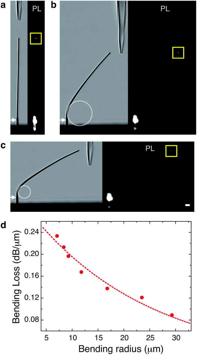 | ||
| Fig. 3 Characterization of bending loss in an MEH-PPV nanowire with a diameter of 295 nm with complete air-cladding. (a–c) The left- and right-hand pictures in (a), (b), and (c) are transmission and photoluminescence (PL) micrographs respectively with decreasing bending radius (a to c). Bending loss is characterized by collecting scattered PL at the upper end of the nanowire (yellow squares), excited by a focused GaN 405 nm laser beam centered at a bottom straight part (white arrows). Scale bar, 3 μm. (d) Bending loss (red circles) against the bending radius fitted with the exponential decay curve (red dashed lines). | ||
In sharp contrast to partial air-cladding in nanowires supported by a substrate,2–4,7 complete air-cladding in our system can be regarded as symmetric cladding like optical fibers. The bending loss, measured for the same nanowire as in Fig. 2, follows double exponential dependency on the bending radius (Fig. 3d), similar to those in optical fibers.20,21 The empirical expression for the attenuation of the ‘curved’ nanowire can be modified to be I = I0exp(−αx)exp(−γl), where γ ∼ C1 exp(−C2R), γ is the attenuation coefficient for bending loss, l is the length of the bent region, R is the bending radius, C1 and C2 are fitting parameters for the geometry and optical properties of the nanowire.7,20 The attenuation by bending is then calculated to be exp(−γl) ∼ exp(−C1(exp(−C2R))) by dividing the output intensity of the bent nanowire by that of the straight one before bending, showing double exponential dependency on bending radius R. Indeed, the bending loss in Fig. 3d is well matched with the double exponential dependency of the attenuation on R, as fitted by the red dashed line. The exponential dependency also agrees with our 3D-FDTD simulation results for bending loss of the nanowires (Fig. S2†) as well as previous 3D-FDTD simulation results,22 both performed under the assumption of complete symmetric air-cladding.
Bending loss involves energy losses caused by the velocity mismatch of the outer evanescent field and the distortion of the modal field,21,23 which also contribute to the enhancement of the evanescent field around the bent region,24,25 as seen in Fig. S3.† For a nanowire supported by a substrate, the enhanced field can induce an increase in energy loss by substrate coupling, possibly leading to an overestimation of the bending loss. Therefore, complete air-cladding is necessary to characterize the actual bending loss of the nanowire, unaffected by substrate effects.
We further investigated scale dependencies of the propagation and bending losses. The propagation loss for a series of nanowires with different diameters in Fig. 4a consistently showed first order exponential dependency of attenuation against the propagation distance. The larger loss in the smaller diameter is attributed to scattering of the enlarged evanescent field by surface contamination, as reported in nanofibers with complete air-cladding.26 The bending loss, characterized for the same nanowires, consistently showed double exponential dependency of attenuation against the bending radius as well (Fig. 4b). The larger loss in the smaller diameter is attributed to coupling of the enlarged evanescent field to the radiation mode,23,27 and agrees with the 3D-FDTD simulation result in Fig. S2.† We believe that diameter and length engineering together with manipulation at complete air-cladding, established in our approach, would also contribute to the understanding of various scale dependent fundamental physics in nanowire photonics.
 | ||
| Fig. 4 Scale dependencies of the propagation loss and bending loss of MEH-PPV nanowires with complete air-cladding. (a) Propagation loss of nanowires with different diameters, 295 nm, 357 nm, and 377 nm. (b) Bending loss for the same nanowires. | ||
To investigate the effect of substrate coupling, we characterized the propagation loss of an MEH-PPV freestanding nanowire with complete air-cladding that was vertically grown on a MgF2 substrate (red circles in Fig. 5). The same nanowire was also characterized after being laid on the substrate (green circles in Fig. 5). MgF2 substrate is widely used to minimize substrate coupling. Showing exponential dependency, the propagation loss per unit length for the nanowire supported by a substrate is very large, 0.29 dB μm−1, almost double that with complete air-cladding, 0.16 dB μm−1. The difference of the attenuation coefficients in the two cases, estimated to be 0.027 μm−1, is attributed to substrate coupling. From this we suggest a simple empirical model for attenuation: I = I0exp(−(α + σ)x), where σ (0.027 μm−1 in Fig. 5) is the attenuation coefficient for additional loss by substrate coupling (Fig. S4†). Explicit estimation of the attenuation coefficient, separating contributions of propagation and substrate coupling, deepens fundamental understanding of light propagation in nanowires and presents practical utility of our nanotechnology in designing nanoscale photonic devices.
 | ||
| Fig. 5 Substrate effect on propagation loss. Propagation losses of an MEH-PPV nanowire with a diameter of 340 nm with complete air-cladding (red circles) and MgF2 substrate supported (green circles). | ||
Conclusions
In conclusion, our results indicate that light propagation in nanowires can be properly understood when complete air-cladding is satisfied. We presented novel nanotechnology that enables characterization of light propagation not only in straight but also in curved active nanowires with complete air-cladding based on three-dimensional growth and remote manipulation of conjugated polymer nanowires. We correctly identified exponential dependencies in propagation and bending losses of MEH-PPV active nanowires. We evidenced that the loss by substrate coupling has first-order exponential dependency with propagation distance. Our method can provide not only fundamental understanding in nanowire photonics but also general utility across nanoscience and nanotechnology.Acknowledgements
This work was supported by the National Research Foundation of Korea (NRF) grant funded by the Korea government (MSIP) (no. 2006-0050683).Notes and references
- R. Yan, D. Gargas and P. Yang, Nat. Photonics, 2009, 3, 569–576 CrossRef CAS.
- M. Law, D. Sirbuly, J. C. Johnson, J. Goldberger, R. J. Saykally and P. Yang, Science, 2004, 305, 1269–1273 CrossRef CAS PubMed.
- F. D. Benedetto, A. Camposeo, S. Pagliara, E. Mele, L. Persano, R. Stabile, R. Cingolani and D. Pisignano, Nat. Nanotechnol., 2008, 3, 614–619 CrossRef PubMed.
- D. O'Carroll, I. Lieberwirth and G. Redmond, Nat. Nanotechnol., 2007, 2, 180–184 CrossRef CAS PubMed.
- X. Xing, H. Zhu, Y. Wang and B. Li, Nano Lett., 2008, 8, 2839–2843 CrossRef CAS PubMed.
- Y. Xiao, C. Meng, P. Wang, Y. Ye, H. Yu, S. Wang, F. Gu, L. Dai and L. Tong, Nano Lett., 2011, 11, 1122–1126 CrossRef CAS PubMed.
- W. Wang, Q. Yang, F. Fan, H. Xu and Z. L. Wang, Nano Lett., 2011, 11, 1603–1608 CrossRef CAS PubMed.
- R. Yan, P. Pausauskie, J. Huang and P. Yang, Proc. Natl. Acad. Sci. U. S. A., 2009, 106, 21045–21050 CrossRef CAS PubMed.
- X. Guo, M. Qiu, J. Bao, B. Wiley, Q. Yang, X. Zhang, Y. Ma, H. Yu and L. Tong, Nano Lett., 2009, 9, 4515–4519 CrossRef CAS PubMed.
- P. J. Pauzauskie, D. J. Sirbuly and P. Yang, Phys. Rev. Lett., 2006, 96, 143903 CrossRef.
- L. Tong, J. Lou, R. R. Gattass, S. He, X. Chen, L. Liu and E. Mazur, Nano Lett., 2005, 5, 259–262 CrossRef CAS PubMed.
- F. Gu, L. Zhang, X. Yin and L. Tong, Nano Lett., 2008, 8, 2757–2761 CrossRef CAS PubMed.
- F. Gu, H. Yu, P. Wang, Z. Yang and L. Tong, ACS Nano, 2010, 4, 5332–5338 CrossRef CAS PubMed.
- P. Domachuk and B. J. Eggleton, Nat. Mater., 2004, 3, 85–86 CrossRef CAS PubMed.
- J. T. Kim, S. K. Seol, J. Pyo, J. S. Lee, J. H. Je and G. Margaritondo, Adv. Mater., 2011, 23, 1968–1970 CrossRef CAS PubMed.
- J. T. Kim, J. Pyo, J. Rho, J.-H. Ahn, J. H. Je and G. Margaritondo, ACS Macro Lett., 2012, 1, 375–379 CrossRef CAS.
- F. Hide, M. A. DiazGarcia, B. J. Schwartz, M. R. Andersson, Q. Pei and A. J. Heeger, Science, 1996, 273, 1833–1836 CrossRef CAS.
- M. T. Bernius, M. Inbasekaran, J. O'Brien and W. Wu, Adv. Mater., 2000, 12, 1737–1750 CrossRef CAS.
- D. Di Camillo, V. Fasano, F. Ruggieri, S. Santucci, L. Lozzi, A. Camposeo and D. Pisignano, Nanoscale, 2013, 5, 11637 RSC.
- J.-I. Sakai and T. Kimura, Appl. Opt., 1978, 17, 1499–1506 CrossRef CAS PubMed.
- A. Yariv and P. Yeh, Photonics: Optical Electronics in Modern Communications (The Oxford Series in Electrical and Computer Engineering), Oxford Univ. Press, Oxford, 2006 Search PubMed.
- H. Yu, S. Wang, J. Fu, M. Qiu, Y. Li, F. Gu and L. Tong, Appl. Opt., 2009, 48, 4365–4369 CrossRef.
- R. Olshansky, Rev. Mod. Phys., 1979, 51, 341–367 CrossRef CAS.
- D. Marcuse, J. Opt. Soc. Am., 1976, 66, 311–320 CrossRef.
- Z. Sheng, D. Dai and S. He, IEEE J. Sel. Top. Quant. Electron., 2009, 15, 1406–1412 CrossRef CAS.
- L. Tong, R. R. Gattass, J. B. Ashcom, S. He, J. Lou, M. Shen, I. Maxwell and E. Mazur, Nature, 2003, 426, 816–819 CrossRef CAS PubMed.
- E. A. J. Marcatili, Bell Syst. Tech. J., 1969, 48, 2103–2132 CrossRef.
Footnote |
| † Electronic supplementary information (ESI) available: Detailed experimental methods; comparison of propagation loss; propagation loss mechanisms; electrostatic manipulation; 3D-FDTD simulations; optical properties of MEH-PPV; experimental setup; PL emission spectra; polarization-resolved PL. See DOI: 10.1039/c4nr00202d |
| This journal is © The Royal Society of Chemistry 2014 |