 Open Access Article
 This Open Access Article is licensed under a
 Creative Commons Attribution 3.0 Unported Licence
Colloidal plasmonic back reflectors for light trapping in solar cells
Manuel J.
Mendes
*a,
Seweryn
Morawiec
ab,
Francesca
Simone
b,
Francesco
Priolo
abc and
Isodiana
Crupi
a
aMATIS CNR-IMM, Via S. Sofia 64, 95123 Catania, Italy. E-mail: manuel.mendes@ct.infn.it
bDipartimento di Fisica e Astronomia, Università di Catania, Via S. Sofia 64, 95123 Catania, Italy
cScuola Superiore di Catania, Via Valdisavoia 9, 95123 Catania, Italy
First published on 14th February 2014
Abstract
A novel type of plasmonic light trapping structure is presented in this paper, composed of metal nanoparticles synthesized in colloidal solution and self-assembled in uniform long-range arrays using a wet-coating method. The high monodispersion in size and spherical shape of the gold colloids used in this work allows a precise match between their measured optical properties and electromagnetic simulations performed with Mie theory, and enables the full exploitation of their collective resonant plasmonic behavior for light-scattering applications. The colloidal arrays are integrated in plasmonic back reflector (PBR) structures aimed for light trapping in thin film solar cells. The PBRs exhibit high diffuse reflectance (up to 75%) in the red and near-infrared spectrum, which can pronouncedly enhance the near-bandgap photocurrent generated by the cells. Furthermore, the colloidal PBRs are fabricated by low-temperature (<120 °C) processes that allow their implementation, as a final step of the cell construction, in typical commercial thin film devices generally fabricated in a superstrate configuration.
1. Introduction
The development of thin film (TF) solar cells grown on inexpensive substrates (e.g. glass, polymeric materials) is regarded as one of the most promising strategies to lower the cost of photovoltaic (PV) electricity generation.1–4 However, the efficiencies of TF cells are still low compared to wafer-based devices, mainly due to their poor near-bandgap light absorption as a consequence of the reduced material thickness. Therefore, the implementation of efficient light trapping (LT) techniques in TF cells is crucial to increase the optical path length of such weakly absorbed light in the cells' material and, thereby, its probability of photocarrier generation.5–10 This allows reducing the cells' thickness without sacrificing absorption, which enables not only lower material costs but also higher conversion efficiencies due to the lower bulk recombination and improved conditions for carrier collection.The most common LT techniques are based on light scattering at rough interfaces, by texturing the substrates and/or electrodes that precede the absorber layers deposition.7,11,12 However, such LT strategy is limited by the increased surface recombination and structural defects in the cell volume which are created during the deposition of thin films on rough surfaces. The defects act as local current drains, degrading not only the short-circuit current (JSC) but also open-circuit voltage, fill factor and reliability of the cells. Therefore, more advanced LT solutions should be developed for TF solar cells, able to increase their optical density without degrading their electrical performance.
While several solutions are under investigation using surface nano-patterning and passivation,2,8,10,11 in the last decade there has been a growing interest in the application of an alternative LT technique based on light scattering from metal nanoparticles (MNPs) sustaining localized surface plasmons (SPs).13–16 A key advantage of the SPs approach is that MNPs can strongly scatter light despite having dimensions much smaller than the illuminating wavelengths; whereas with the conventional texturing approach the dimensions of the textures should be of the order of magnitude of the wavelengths in order to scatter efficiently, making it difficult to provide LT in the longer wavelengths (near-infrared, NIR) which are those more poorly absorbed by the cell material.9,17,18 Moreover, the resonant scattering properties of MNPs can be tuned across the visible and NIR spectrum by changing their geometry,19,20 allowing their application not only in distinct types of solar cell designs but also in biosensing, LEDs, enhanced spectroscopy, near-field microscopy, optical antennas, optical signal processing, etc.
In initial implementations, MNPs were placed at the front surface of the solar cells or inside the absorber layer.13,14,21 In both configurations the application of MNPs reduces the cell efficiency due to their absorption losses, backscattering of light and non-radiative recombination of the photo-generated carriers at the metal–absorber interface. Thus, it is preferential to adopt what is known as a plasmonic back reflector (PBR) configuration, in which the MNPs are placed at the rear of the cells incorporated in the back reflector/contact.13,22–25 In such a configuration the MNPs interact only with the long-wavelength light which is not absorbed in the first pass through the cell material. Such light is scattered by the nanoparticles and returns to the cell (either directly or via the back mirror layer) at oblique angles, thus traversing a longer path inside the absorber region. The PBR configuration also allows the decoupling of LT and anti-reflection effects, enabling the use of a traditional anti-reflection coating on the front surface of the cells.
Recently, PBRs have been shown to significantly improve the efficiency of TF hydrogenated amorphous silicon (a-Si:H)25,26 and microcrystalline silicon (μc-Si:H)27 solar cells, at the level of state-of-the-art surface texturing. For instance, in a-Si:H cells an increase of 27% in the near-bandgap (550–800 nm wavelength range) photocurrent and 25.4% in the efficiency was achieved with PBRs, as compared to respectively 25.7% and 23.8% obtained with texturing.25 The MNP structures implemented in the PBRs are usually formed via a solid-state dewetting (SSD) process, by deposition of a thin precursor film of silver (Ag) followed by annealing at temperatures of 300–500 °C.13,23,24 This forms self-assembled drop-like Ag particles with a flattened roughly hemispherical shape. Although the SSD process is simple, cheap and suitable to implement in industrial production, it has the following main drawbacks:
(1) Broad dispersion in the particles size and shape. It is difficult to control the morphology of the obtained nanostructures which prevents obtaining the optimal resonant scattering at the spectral regions of interest.
(2) The unavoidable presence of small (<50 nm) particles, MNP geometries with high degrees of curvature and too high MNP surface coverage result in high dissipative light losses (parasitic absorption).17
(3) The high temperatures required for the annealing step forbid the formation of the MNP structures as a post-process on top of TF Si cells, since the Si–H bonds are damaged at temperatures ≳200 °C.28 Therefore, SSD-formed PBRs cannot be applied in commercial TF cells usually assembled with a superstrate configuration, which is the present industrial standard.11
The novel approach presented in this work is able to solve the aforementioned issues by using MNPs synthesized in colloidal solution and later patterned in uniform arrays, employing a controlled wet-coating technique.16,29 Such a technique allows the self-assembly of mono-sized spherical MNPs (see bottom of Fig. 1) onto the surface of several materials via scalable, inexpensive and low-temperature (<120 °C) processes that can be executed at the last stage of the solar cell construction and, therefore, implemented in both substrate and superstrate cell designs. The relatively low fabrication temperature also enables the application of colloidal PBRs in a broader range of solar cell substrates, such as in polymeric materials (e.g. polyethylene-naphtalate,3 polyimide4) that can be used in flexible TF cells manufactured by roll-to-roll processes. Besides, this method allows control on the inter-particle spacing of the deposited MNPs and their surface coverage.
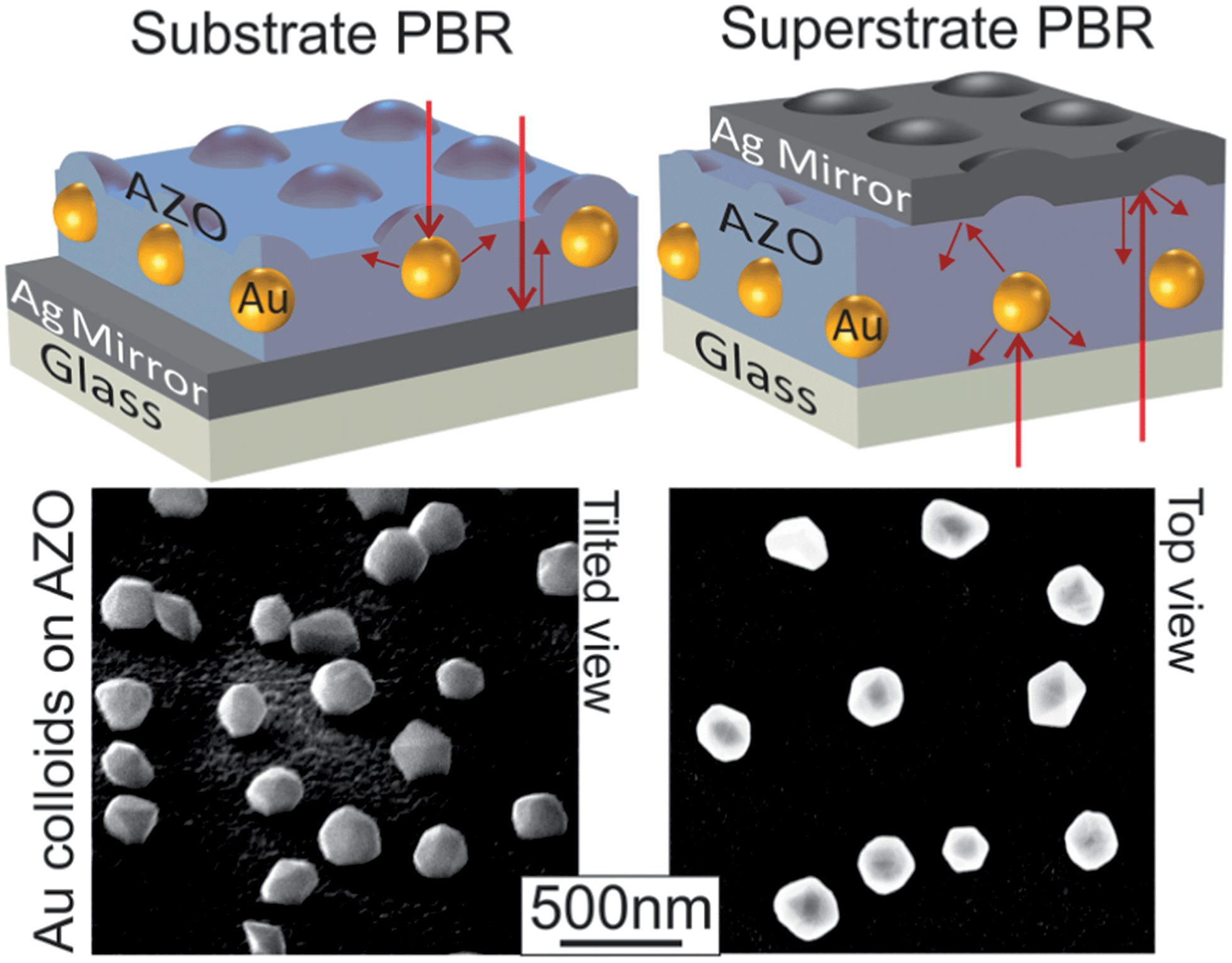 | ||
| Fig. 1 Top: sketch of the two PBR configurations studied in this work. The left PBR is intended for the bottom contact of TF cells with a substrate configuration, whereas the right PBR is for cells with a superstrate configuration. In the former configuration the cell material would be placed onto the PBR, whereas in the latter it would be placed between the glass substrate and the AZO. Bottom: tilted and top-view scanning electron microscopy images of Au colloids with 200 nm diameter patterned on AZO. | ||
The chemical synthesis of colloids is currently the most reliable method to produce macroscopic amounts of nanoparticles with monodisperse physical properties, in order to minimize the inhomogeneous broadening of their collective response in functional materials.16,22,30 The metals that allow strongest SP response are Ag and gold (Au), due to their low imaginary permittivity. Even though Ag would represent lower material costs, for the present studies Au colloids were used due to their high mono-dispersion in size and shape as well as chemical, thermal and environmental stability relative to Ag. We have observed that the deposited Au colloidal arrays are not affected by oxidation, as their optical properties match those determined from electromagnetic modeling with Mie theory and remain invariant over indefinitely long time. In addition to providing LT, Au MNPs may also lower the Schottky barrier and improve the work function matching at the interface between the PBR structure and the absorber material of the cell.22
The substrate and superstrate PBR configurations analyzed in this work are sketched in the top of Fig. 1. They are supported on glass substrates and are composed of an Ag mirror and a transparent conductive oxide (TCO) layer, made of aluminum zinc oxide (AZO), in which the MNPs are embedded.
The results described in this paper reveal that colloidal substrate-type PBRs can provide pronounced light diffusion and reflection, comparable to the best state-of-the-art PBRs formed with SSD. The superstrate PBRs exhibit relatively worse optical performance, due to the unavoidable roughness in the Ag mirror, but should still allow considerable photocurrent enhancement in double-junction TF Si solar cells as those currently being commercialized.
2. Theoretical background
Sub-wavelength metal particles can act as antennas at optical frequencies, gathering light from their surroundings and scattering it to the far-field over a broad angular range. This effect can be particularly pronounced in MNPs made of noble metals such as Ag or Au, due to their low imaginary permittivity, when the wavelength of the illuminating light matches the MNPs' SP resonances. When such resonances are excited they can decay radiatively, resulting in scattered light, or non-radiatively resulting in absorption. The sum of absorption and scattering is the extinction whose maxima occur at the SP wavelengths. In order to enhance LT in solar cells the MNPs should exhibit low absorption and large scattering in the visible (VIS) and NIR.17,19An important advantage of colloidal MNP structures is that their optical response closely matches single-particle electromagnetic computations, since the colloids are synthesized with highly mono-dispersed sizes and spherical shapes, and with pure crystalline materials. Therefore, Mie theory formalisms can accurately calculate the scattering properties of such structures when they are embedded in a homogeneous medium.16,26,31 Even though MNPs incorporated in PBRs are not surrounded by a uniform medium (see Fig. 1), Mie theory can still be used for a first-order analytical prediction of their preferential sizes.24,26 The normalized scattering (QSCA) and absorption (QABS) cross-sections are calculated by dividing, respectively, the total scattered and absorbed power by the incident intensity and by the geometrical cross-section of the particle. The sum of QSCA and QABS is the normalized extinction cross-section (QEXT).
The performance (Γ) of a MNP for light scattering can be evaluated by the quantity Γ300–2000 nm, given by the ratio between the average values of QSCA and QEXT determined by integrating the spectra of these quantities along the main solar wavelength range (300–2000 nm).17,26 This quantity is shown in Fig. 2 as a function of the MNP diameter (D), considering single Au nanospheres embedded in AZO. The QSCA and QABS spectra are shown in the insets for three particle sizes. QABS is higher than QSCA for particles with sizes up to about 50 nm, but as the diameter increases the MNPs radiate more efficiently and for sizes over 100 nm the extinction is dominated by scattering.
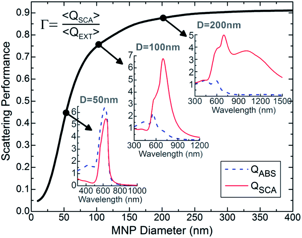 | ||
| Fig. 2 Scattering performance (Γ) of single spherical Au NPs immersed in a AZO medium, evaluated along the 300–2000 nm spectral range, as a function of the NPs diameter. The insets show the QSCA and QABS of particles with 50, 100 and 200 nm diameter (D). The quantities were computed with an analytical Mie theory formalism.31 | ||
As seen in the insets of Fig. 2, MNPs with sizes below 100 nm sustain a single dipolar SP mode in the scattering spectra, while bigger particles exhibit additional higher order modes. As the particle size increases, depolarization retardation effects and the higher number of multipolar modes broaden the QSCA spectrum towards the NIR and hinder the efficiency of the resonant scattering process, which causes the saturation of the Γ curve.14,23,24,32 Therefore, Au spheres with a size of 100 nm or higher are potentially favorable scatterers for LT application, but for sizes above 200 nm their performance is not expected to further improve significantly.13,26 As such, and in order to minimize the roughness and material costs of the LT structure, the preferential MNP diameters should be in the range of 100–200 nm.
PBRs are particularly promising for application in TF Si solar cells, where the requirement for LT is strong since their absorption coefficient decreases substantially with increasing wavelength.11,33 In these cells, LT is primarily needed for wavelengths above 600 nm since for shorter wavelengths the light can be entirely absorbed in a first pass through the cell material or by specular reflection from a rear flat mirror.13,34 For the case of typical single-junction a-Si:H cells, the Si layers have a thickness of about 300 nm and can only absorb light with a wavelength up to ∼800 nm. As such, due to the narrow LT spectral window of a-Si:H cells, particle sizes close to 100 nm are preferable since they produce a sharp and relatively high dipolar QSCA peak centered at the 600–800 nm range, as shown in the middle inset of Fig. 2. For the case of single-junction μc-Si:H or double-junction a-Si:H/μc-Si:H solar cells, as those currently dominant in the TF PV market, the LT window (∼600–1150 nm) extends further to the bandgap of c-Si. Therefore, for these cells a bigger particle size is preferable, such as the D = 200 nm MNP shown in the right inset of Fig. 2, that sustains a broader and more red-shifted QSCA dipolar peak and additional higher-order peaks at shorter wavelengths.
Colloidal Au nanospheres can be engineered to have QSCA maxima that greatly exceed unity in an AZO medium, as shown in the insets of Fig. 2. So, even an incomplete surface coverage of the particles can lead to scattering of all incident light.17 When the particles are located close to the solar cell material, a significant fraction of their scattered light is coupled to the high refractive index medium (e.g. Si) of the cell over a large angular range, increasing the path length of the light in this medium and, consequently, the generated photocurrent.23,35
3. Experimental methods
Crystalline gold colloids can be synthesized in aqueous solutions with an approximately spherical shape and any mono-disperse size from tens to hundreds of nanometers. The colloidal solutions used here were purchased from BBI solutions and contain Au MNPs stabilized in water by organic capping molecules with negatively charged end-groups attached to their surface. The negative surface charge causes the particles to repeal each other and prevents their aggregation in water.30A wet-coating technique was developed in this work to deposit such colloids, with sizes in the 100–200 nm range, on AZO layers. The technique consists of chemically functionalizing the AZO surface with a self-assembled monolayer (SAM) of molecular linkers with positively charged end-groups that attract the negatively charged particles.16,29 During the wet-coating the MNPs are free to diffuse across the surface, so once a particle adheres to the surface linkers its negative charge will repeal other MNPs from settling at the same location. In this way, a uniform array of mostly isolated particles is formed (as shown in Fig. 3) that can extend throughout the area of arbitrarily large samples. The average inter-particle distance is proportional to the MNPs' surface charge density; so it can be tuned by changing the capping agent, solvent liquid or pH of the solution. This allows the regulation of the particle density and level of aggregation on the surface,30,36 which is hard to achieve with the conventional technique of MNP formation by SSD discussed in Section 1.
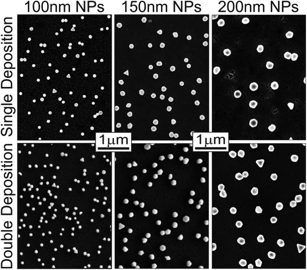 | ||
| Fig. 3 SEM images of Au NP arrays deposited with the wet-coating method developed in this work. The distributions were obtained with either one (top) or two (bottom) sequential depositions of particles with distinct diameters (100, 150 and 200 nm). The MNPs surface coverage increases from 4–5% in a single deposition to ∼8% in a double deposition. | ||
The patterning method was applied in AZO-coated glass samples, with 2.5 × 2.5 cm2 area, and consists of the following steps:
(1) The AZO surface is hydrophilized by treating it in ultraviolet ozone (UVO) for 15 min and dipping it in DI water. This favours the formation of the SAM performed next.36
(2) The sample is dehydrated, by dipping in ethanol, and the surface is functionalized by immersion in a 1% dilution of APTMS [(3-aminopropyl)trimethoxysilane] in ethanol for 1 h. This forms a positively charged amine-terminated SAM uniformly covering the AZO surface.29,30 In the literature, such functionalization is usually performed with aqueous amino–silane solutions, but it was observed that such solutions can partially remove the AZO layer during the immersion. Therefore, it is preferable to use alcohol solvents which preserve the AZO quality in this treatment.
(3) The sample is baked for 30 min at 110–120 °C to strengthen the adhesion of the APTMS molecules to the AZO.
(4) The sample surface is fully covered with 1.2 ml of the MNP solution for 2 h. During this period the negatively charged MNPs are uniformly deposited onto the APTMS-modified AZO surface.
(5) The sample is rinsed in DI water to remove the excess MNP solution and finally dried.
This electrostatic-based patterning approach is adaptable to any particle and substrate material as long as the surfaces can be functionalized with oppositely charged molecular linkers. Similar methods have been applied to different substrate (e.g. ITO,36 Si, GaAs,29 glass16) and colloidal (e.g. Ag29) materials. However, most contributions in the literature only report on the formation of arrays of small (D < 50 nm) MNPs onto SAM-functionalized surfaces, which are not suitable for PV LT as discussed in Section 2. This is the first time, to our knowledge, that uniform arrays of large (D > 100 nm) Au MNPs, ideal for far-field scattering, are patterned onto a TCO material. Colloids with such relatively big sizes tend to agglomerate into multilayer or three-dimensional aggregates, rather than forming monolayer single-particle arrays, due to their large van der Waals attractions and the easier loss of stabilizing capping molecules on their facets.30 The wet-coating method used here is able to pattern MNPs with the big sizes favorable for PV LT (as described in Section 2) due to a careful selection and control in the chemical treatments of the surface (hydrophilization, SAM functionalization, drying conditions, etc.).
The top scanning electron microscopy (SEM) images in Fig. 3 show three distributions of Au MNPs obtained with colloidal solutions of 100, 150 and 200 nm particle diameters, deposited on AZO. The surface coverage, determined from a large number of SEM images, is around 4–5% for the three particle sizes. The images were acquired with Zeiss Supra 25 Field-Emission SEM equipment.
The wet-coating technique developed here allows the adjustment of the particle density on the surface via sequential depositions, by repeating the steps listed above as many times as desired. The bottom images in Fig. 3 show the distributions of Au NPs after a second deposition, which increases the surface coverage to ∼8% similarly for the three particle sizes. This provides a more complete interaction between the incident light and the MNPs array. However, even though the MNPs are still predominantly present as individual isolated particles, the second deposition slightly increases the particle aggregates and inter-particle interactions which alter the MNPs plasmonic response and contribute to the light losses (parasitic absorption).21,23
The AZO and Ag films composing the structures analysed in this work were deposited with 13.56 MHz RF magnetron sputtering equipment, under an Argon pressure of 10−2 mbar, using respectively 225 W and 30 W of applied power.
All the optical measurements were performed with a Varian Cary 500 double-beam scanning UV-Vis-NIR spectrophotometer equipped with a 4 inch integrating sphere.
4. Optical properties of colloidal plasmonic back reflectors
4.1 Comparison with Mie theory
The optical response of the obtained Au nano-sphere arrays can be directly compared with Mie theory calculations by embedding the particles in a homogeneous medium. The results are plotted in Fig. 4a which shows the total (reflected plus transmitted) diffuse light from a 100 nm Au MNP array embedded in AZO, together with the QSCA curve of a single particle (that is in the D = 100 nm inset of Fig. 2).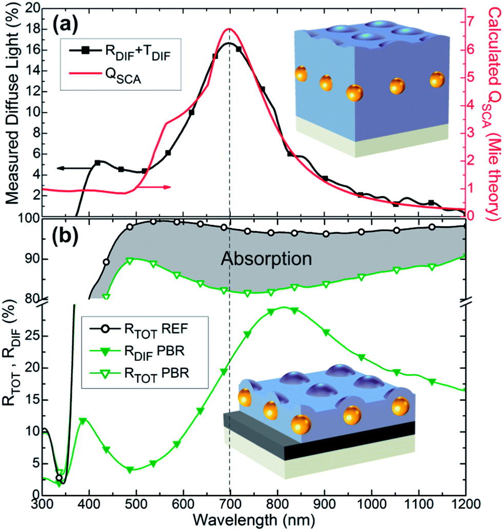 | ||
| Fig. 4 (a) Measured total diffuse light (left axis), given by the sum of the diffuse reflectance (RDIF) and transmittance (TDIF), from a D = 100 nm Au MNP array deposited on a 500 nm thick AZO layer supported on glass and then covered with a 250 nm AZO top layer. The peak of diffuse light occurs at the dipolar SP resonance of the MNPs and matches the QSCA peak (right axis) calculated with Mie theory considering a particle immersed in AZO. (b) Total (RTOT) and diffuse reflection from a substrate-type PBR (green curves), with the structure: glass substrate/100 nm Ag/35 nm AZO/Au MNPs/70 nm AZO, containing one deposition of D = 100 nm Au MNPs. The RTOT of a reference BR (black curve) without the MNPs is shown for comparison. The difference (grey area) between the reference RTOT and the PBR RTOT corresponds to the parasitic light absorption caused by the MNPs. | ||
The AZO layers embedding the particles are thick enough to prevent the MNPs from significantly interacting with the glass substrate and air interfaces, so the medium surrounding the nanoparticles can be considered uniform. Therefore, the measured diffuse light matches exactly the QSCA peak, computed with Mie theory, corresponding to the dipolar SP resonance of the MNPs. This result of Fig. 4a supports several relevant aspects: (1) the physical properties (material, size, shape) of the Au MNPs are mono-disperse in the array and correspond precisely to the expected ones. (2) The distances between the deposited particles are long enough to prevent considerable inter-particle interactions. (3) The sputtering deposition of the AZO material on top of the MNPs does not affect the particles morphology.22
4.2 Substrate PBRs
As pointed out in Section 1, the preferential location of the MNP arrays in solar cells is in the rear contact, between the absorber layers and the back reflector (BR). Typical BRs of TF Si cells are composed of a ∼100 nm thick Ag layer (the mirror) separated from the Si layers by an AZO layer with thickness of 50–100 nm. The Ag mirror, apart from being a highly conductive back contact, improves LT since light that is not initially coupled to the cells is given multiple reflection opportunities. The AZO acts as an efficient adhesion and barrier layer, preventing possible carrier recombination and diffusion of metallic impurities to the cell material.37 Therefore, the MNPs should be positioned inside such a protective AZO layer.11,18 The thickness of AZO separating the MNPs from the absorber layers should be thin (on the order of tens of nanometers) to allow a good coupling of the scattered light to the high-index cell material.15,19,25The layer structure of the two types of PBRs developed in this work is shown in Fig. 1. We start by analyzing substrate-type PBRs which is the configuration employed in conventional state-of-the-art PBRs made with SSD-formed Ag NPs.13,25–27
Colloidal PBRs aimed for TF cells with a substrate configuration were formed with the structure depicted in the top-left of Fig. 1: glass substrate/Ag mirror (100 nm)/AZO spacer layer (t)/Au MNPs array/AZO cover layer (70 nm). The MNPs were deposited employing the wet-coating procedure described in Section 3, either with one or two sequential depositions (see Fig. 3).
Fig. 4b shows the diffuse (RDIF) and total (RTOT) reflectance obtained with a substrate PBR composed of a single deposition of Au colloids with 100 nm diameter. As a reference, the RTOT of a BR without MNPs is also shown. The PBR has a lower RTOT than the reference BR due to the loss of light caused by the MNPs (marked by the grey area termed absorption), as a consequence of parasitic absorption inside their material and possible dissipative interactions between the MNPs and the surrounding media.34 The peak of such absorption is blue-shifted from the scattering peak of RDIF, as occurs with the QABS and QSCA peaks in the D = 100 nm inset of Fig. 2.
The presence of the Ag mirror causes a red-shift of the RDIF peak relative to the peaks in Fig. 4a corresponding to particles embedded in AZO and computed with Mie theory. Besides, it enhances the peak intensity by a factor of almost two. This substantial enhancement indicates that the Ag mirror in the PBR not only reflects the transmitted diffuse light coming from the MNPs, but also originates a constructive interaction with the particles that increases their scattered power relative to the case when they are immersed in a homogeneous medium.34 Therefore, the separation between the nanoparticles and the Ag mirror is a crucial parameter in PBRs, which will be analyzed in more detail further below.
The amount of light scattered by the nanoparticles can be enhanced by increasing their density in the array, via two sequential colloidal depositions (see Fig. 3). The particles from the second deposition settle preferentially in the empty areas left by the particles of the first deposition, due to the electrostatic repulsion between the colloids caused by their negatively charged capping molecules. As such, the surface coverage of individual particles is increased leading to a considerable enhancement in the diffuse light of the PBR.
Fig. 5 shows the results of three PBRs with the same layer structure as that of Fig. 4b but with two sequential depositions in the Au MNPs array, composed of particles of three distinct diameters. The RDIF peak of the PBR with 100 nm MNPs is enhanced by a factor of 1.37, relative to that of Fig. 4b with a single deposition of nanoparticles, due to the higher number of individual MNPs. However, the RTOT is reduced by a factor of ∼0.87 and the RDIF peak becomes slightly broader and red-shifted as a consequence of the increased interparticle interactions.
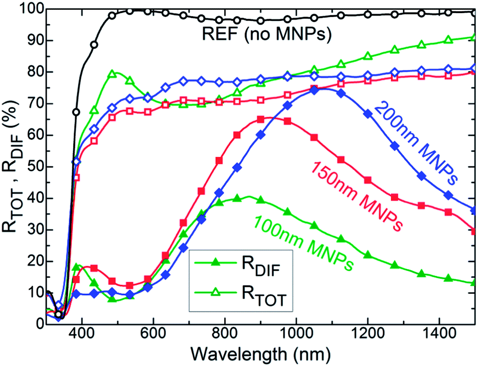 | ||
| Fig. 5 Total (open symbols) and diffuse (filled symbols) reflectance of substrate PBRs composed of two depositions of Au MNPs with distinct diameters (100, 150 and 200 nm) and with the same layer structure as that of Fig. 4b. The total reflectance of a reference BR (open circles), with the same structure but without MNPs, is shown for comparison. | ||
As the MNP size increases to 150 and 200 nm the scattered light is pronouncedly enhanced and the RDIF maxima reach much higher values of 66% and 75%, respectively. These values are similar to those of the best-performing PBRs fabricated until now, with the conventional SSD method, implemented in TF Si cells.25–27 The increase in the MNPs diameter also leads to a broadening and red-shift of the plasmonic resonances, as discussed in Section 2. Therefore, the 150 and 200 nm particles produce a much broader RDIF coverage of the NIR spectral range than the 100 nm particles.
As previously mentioned, the performance of PBRs is particularly sensitive to the spacing between the Ag mirror and the MNPs array. When a MNP is located in the proximity of a mirror, the interference between the incident electric field and the fields reflected from the mirror (both scattered and not scattered by the MNP) modifies the driving field that polarizes the particle and is particularly sensitive to the MNP–mirror separation distance and to the illumination wavelength.34 Therefore, for a given MNP distribution, the scattering spectrum of the PBR can be optimized by tuning the AZO spacer thickness to allow the highest possible constructive interference in the spectral range of interest.
We analyzed the reflective properties of PBRs with different thicknesses (t) of the spacer AZO layer deposited between the mirror and the particles. The results are presented in Fig. 6 which shows the values of the average total (〈RTOT〉) and diffuse (〈RDIF〉) reflectance in the 600–1150 nm wavelength range, corresponding to the LT window of single-junction μc-Si:H or double-junction a-Si:H/μc-Si:H solar cells. The PBRs contain a double deposition of D = 100 nm Au MNPs and the layer structure shown in the inset of Fig. 6. It can be observed that the thinner the spacer the higher the RDIF due to increased interaction between the MNPs and the Ag mirror, which boosts the scattering efficiency of the nanoparticles. The fact that RTOT decreases with the spacer thickness means that such an interaction also contributes to the parasitic absorption of the overall PBR. The PBRs of Fig. 4b and 5 have an AZO spacer layer with the smallest thickness plotted in Fig. 6 (t = 35 nm), which is the thickness that yields the highest RDIF and lowest RTOT from the set of PBRs investigated in Fig. 6. For comparison, two points are shown in the figure with the 〈RTOT〉 and 〈RDIF〉 of a PBR with that same spacer thickness but with a D = 100 nm MNP array formed from a single deposition. As expected, since this PBR has less MNP surface coverage, its RDIF is lower than that with a double MNP deposition but its RTOT is higher due to reduced parasitic absorption.
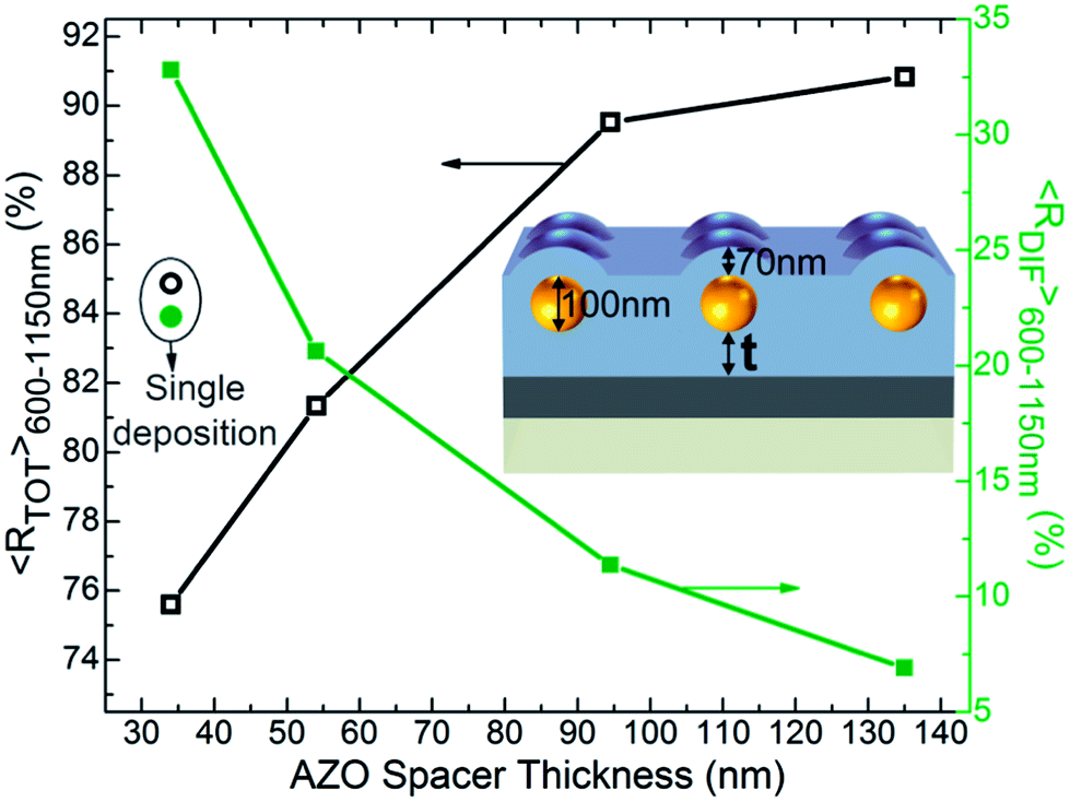 | ||
| Fig. 6 Average RTOT (open symbols) and RDIF (filled symbols), along the 600–1150 nm wavelength range, for PBRs with distinct AZO spacer thickness (t). The structure of the PBRs is sketched in the inset and its MNP array is composed of a double deposition of D = 100 nm Au colloids. The two circular symbols at t = 35 nm show the average RTOT and RDIF of a PBR with the same structure but with only a single deposition of MNPs. | ||
The trends obtained in Fig. 6 are in accordance with those determined by Sesuraj et al.34 Nevertheless, Sesuraj et al. also observed that for small (<40 nm) spacer thicknesses RDIF starts decreasing and RTOT increasing with decreasing t. So, irrespective of their size, the MNPs' radiative efficiency becomes quite low at very close (t < 10 nm) distances to the mirror and there is, therefore, an optimal distance around 40 nm where the scattered power peaks. Hence, the smallest spacer thickness investigated in this work (t = 35 nm) should be close to the optimum.
4.3 Superstrate PBRs
Apart from the high monodispersion in size and shape of colloidal MNPs, one of their key technological advantages is that MNP structures can be formed by low temperature (<120 °C) processes. Therefore, as mentioned in Section 1, colloidal PBRs can be integrated in a final post-processing step in the fabrication of solar cells with a superstrate configuration, which is the configuration of the TF cells that are currently under industrial production.11,12In this work we studied the performance of PBRs, aimed for superstrate cell configurations, with the structure depicted on the top-right of Fig. 1: glass substrate/AZO bottom layer (250 nm)/Au MNPs array/AZO spacer layer (t)/Ag mirror (100 nm). The MNPs were deposited employing two sequential particle depositions.
Fig. 7a shows the RTOT and RDIF of two such PBRs, measured from the glass side, with D = 100 nm Au MNPs and distinct AZO spacer thickness. These PBRs have a much higher haze in reflection (RDIF/RTOT) than the substrate PBR shown in Fig. 5 with 100 nm MNPs, but a lower total reflection. This is due to the roughness induced in the top Ag mirror caused by the conformal growth of the material over the AZO-covered MNPs. The roughness in the Ag mirror can be visualized in the SEMs of Fig. 7b, showing both semi-hemispherical hills caused by the MNPs' shape and smaller bumps over all the surface (see SEM with a higher magnification) caused by the roughness of the AZO material. These two types of roughness considerably increase the overall parasitic absorption in the PBR, and reduce the constructive interference of the electric fields reflected from the mirror on the driving field that polarizes the MNPs. Both these effects worsen the scattering performance (i.e. diffuse light) of these PBRs relative to the case of PBRs with a flat mirror, as those of Section 4.2. Consequently, superstrate PBRs exhibit an opposite trend relative to the AZO spacer thickness than that observed in Fig. 6, because the thicker the spacer the flatter the mirror. Therefore, the RDIF of this type of PBRs increases with higher AZO spacer thickness, as observed in the examples of Fig. 7a. PBRs fabricated with thinner AZO spacers exhibited worse performance.
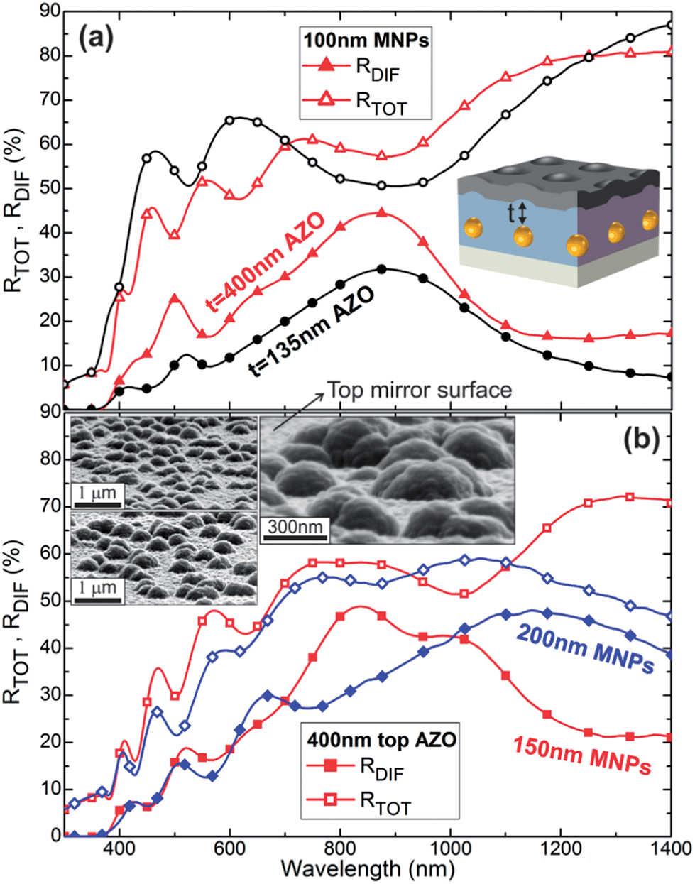 | ||
| Fig. 7 Total (open symbols) and diffuse (filled symbols) reflectance of PBRs aimed for solar cells with a superstrate configuration, made with a double deposition of Au MNPs. (a) Reflectance of two PBRs made with 100 nm diameter MNPs and two distinct AZO spacer thicknesses (t) of 135 and 400 nm. (b) PBRs with t = 400 nm and two distinct MNP diameters of 150 and 200 nm. The MNPs' shape induces hills on the top mirror, as seen in the SEM images. The top-left SEM corresponds to the 150 nm diameter PBR, whereas the other two SEMs correspond to the 200 nm one at distinct magnifications. | ||
Bigger Au MNP sizes produce an enhanced scattering performance, as observed in Fig. 2 and 5, but in superstrate PBRs they also increase the hills in the Ag mirror (see SEMs in Fig. 7). So, as shown in the results of Fig. 7b, the beneficial effects of increasing the MNP diameter to 150 and 200 nm are hindered by the roughness that they generate in the mirror. Thus, the enhancement in RDIF when the MNP diameter is increased from 100 to 150 nm is much lower than that of Fig. 5, and there is even a slight reduction in the maximum RDIF when the diameter is further increased from 150 to 200 nm.
5. Discussion of results
The optical properties of the PBRs analyzed in the previous section are affected when the structures are implemented in solar cells, since the light scattered from the MNPs and Ag mirror changes when they are placed close to a high refractive index medium such as silicon. The higher refractive index of such medium increases the amount of scattered light coupled to and trapped in the cell, but it also generates additional reflected fields interacting with the MNPs plus mirror system that shall impose a trade-off on the optimal thickness of the AZO layer separating the particles from the cell material.19,23,35 These effects have not been considered in this study since it is mainly aimed at analyzing the light scattering elements regardless of the specific absorbing/receiving elements to which they can be coupled to. Nevertheless, in previous studies of PBRs implemented in Si solar cells,18,22,23,25–27 it has been observed that the spectra of diffuse light measured in the PBR structures alone correlate with the extinction enhancement that they produce, for wavelengths from 600 nm towards the IR, when implemented in the cells. Such light extinction amplification is then observed to match the enhancement in the quantum efficiency spectrum of the devices, which implies that the additional light absorption in the cells caused by the PBRs is mainly translated into photocurrent, with a smaller percentage going into optical losses. Therefore, the optical results presented in Section 4 and summarized in Table 1 constitute reasonable quantities for a preliminary evaluation of the fabricated PBRs in view of their application for PV light trapping.| Au NPs diameter | Substrate PBRs | Superstrate PBRs | ||
|---|---|---|---|---|
| 〈RDIF〉 | 〈RTOT〉 | 〈RDIF〉 | 〈RTOT〉 | |
| 100 nm | 32.9% | 75.7% | 32.1% | 62.6% |
| 150 nm | 51.5% | 72.4% | 37.8% | 54.6% |
| 200 nm | 52.0% | 77.8% | 35.8% | 54.0% |
Table 1 shows the average values of RDIF and RTOT, along the LT spectral window of TF Si cells, of the substrate and superstrate PBRs analyzed respectively in Fig. 5 and 7. It is clear that the best-performing PBRs are those with the conventional substrate configuration, formed with 150 and 200 nm particles. Such colloidal PBRs exhibit an 〈RTOT〉 and 〈RDIF〉 similar to those of the best state-of-the-art PBRs, formed with the conventional SSD method,26,27 despite having a much lower MNP surface coverage (∼8%). Even though SSD-formed PBRs exhibit a high surface coverage (∼20–40%), the average QSCA of their MNPs is decreased by the presence of small (D < 100 nm) particles which increase the parasitic absorption.23,24 The D = 150 and 200 nm PBRs of Fig. 5 are formed with highly monodisperse distributions of high-QSCA nanospheres. So, they exhibit a maximum RDIF close to RTOT, which implies that such structures provide an almost complete interaction with the incident light at the peak plasmonic resonance despite the relatively low concentration of MNPs on the surface.
In view of the above, the 150 and 200 nm substrate PBRs are expected to produce improvements in TF Si cells similar to those (∼20% JSC enhancement) attained with state-of-the-art SSD-formed PBRs and conventional texturing.26,27 Such enhancements are still far from the theoretical ideal case of Lambertian reflective structures, which can provide up to 42% and 100% increase in JSC in typical 300 nm-thick amorphous and 2 μm-thick crystalline Si TF cells, respectively.2 The discrepancy between the real enhancements and those envisaged theoretically is mainly attributed to the parasitic absorption produced by the MNPs.24 Therefore, the minimization of such absorption losses is an essential goal for further improvement of plasmonic LT for PV.
The PBRs with the novel superstrate configuration do not perform so well as the substrate ones due to the roughness induced in the rear mirror layer, but they still provide 〈RDIF〉 and 〈RTOT〉 in the NIR spectral region comparable to those achieved with standard SSD-formed PBRs reported in the literature.18,25,34 Nevertheless, since superstrate PBRs are to be assembled on top of previously fabricated cells, they offer the important technological advantage of not introducing any roughness in the absorbing cell layers. As indicated by simulation and experimental results, large MNP sizes are preferable for efficient light scattering but, in a substrate configuration, they also contribute to the roughness in the TF cell material which can increase the current, voltage and fill factor losses via surface and bulk carrier recombination, as occurs with traditional texturing approaches.11,17,19 In superstrate PBRs the photocurrent-generating cell layers remain perfectly flat regardless of the MNP sizes used for LT, therefore this is the only configuration that allows maximizing the light absorption enhancement without compromising the electrical properties of the cell material.
6. Conclusions
Solution-based self-assembly provides a simple, scalable and inexpensive method for producing ensembles of colloidal MNPs in a controllable manner, in order to exploit their collective properties in functional devices. The colloidal Au nanoparticles used in this work were synthesized and patterned by simple and low-cost wet chemical methods that can be straightforwardly scaled up for full-size solar cell integration in mass manufacture. The particle deposition method developed here, driven by electrostatic interactions, is a self-controllable and highly parallel process which should allow the simultaneous fabrication of many devices. As an example, square-meter sized panels can be patterned by sequentially immersing them in baths of the appropriate solutions described in Section 3.The fabrication and optical studies presented here show that colloidal PBRs are promising for application in TF PV. Not only for the technological possibilities that they enable due to the use of low-temperature manufacturing processes, but also for the fact that colloidal synthesis allows the integration of MNP structures with better physical properties (crystalline material, monodisperse size and shape distribution, controllable inter-particle distance, etc.) than those of conventional PBRs composed of metal nano-drops formed by solid state dewetting of thin films. Therefore, the application of such a novel colloidal LT approach in solar cells can allow higher conversion efficiency enhancements than those already observed with conventional SSD-formed PBRs.
The obtained results indicate that colloidal PBRs are particularly suited for implementation in TF Si cells, either composed of a μc-Si:H single junction or a a-Si:H/μc-Si:H double junction, whose LT window (600–1150 nm) matches the extension of the broad diffuse reflectance peaks of the PBRs. Nevertheless, their optical properties can also be adapted to other types of solar cells that can benefit from LT in the IR spectral range, by adjusting the MNPs geometry and/or MNPs–mirror separation distance, such as intermediate band solar cells.6,16,20
A key solution for industrial implementation allowed by colloidal PBRs is the possibility to integrate them in a superstrate cell configuration, where they are assembled as a final step on top of the previously grown solar cell layers. This would not be possible with the conventional SSD PBRs due to the relatively high temperatures required for their fabrication. The scattering performance of superstrate PBRs is limited by the roughness that the AZO-covered MNPs induce in the rear silver (Ag) mirror, so it could be substantially improved by developing a novel process able to flatten the mirror, for instance by nano/micro-scale polishing the top AZO layer.38
Acknowledgements
This work was funded by the EU FP7 Marie Curie Action FP7-PEOPLE-2010-ITN, through the PROPHET project (Grant no. 264687), and by the MIUR project Energetic (Grant no. PON 02_00355_3391233).References
- H. Aguas, et al., Silicon thin film solar cells on commercial tiles, Energy Environ. Sci., 2011, 4(11), 4620–4632 CAS.
- A. Bozzola, M. Liscidini and L. C. Andreani, Photonic light-trapping versus Lambertian limits in thin film silicon solar cells with 1D and 2D periodic patterns, Opt. Express, 2012, 20(S2), A224–A244 CrossRef PubMed.
- O. Cubero, et al., Latest results on stabilized flexible thin film silicon solar cells, in 23rd European Photovoltaic Solar Energy Conference, Valencia, Spain, 2008, pp. 2101–2104 Search PubMed.
- A. Chirilă, et al., Highly efficient Cu(In,Ga)Se2 solar cells grown on flexible polymer films, Nat. Mater., 2011, 10(11), 857–861 CrossRef PubMed.
- M. J. Mendes, et al., Light concentration in the near-field of dielectric spheroidal particles with mesoscopic sizes, Opt. Express, 2011, 19(17), 16207–16222 CrossRef PubMed.
- A. Mellor, et al., Upper limits to absorption enhancement in thick solar cells using diffraction gratings, Prog. Photovoltaics, 2011, 19(6), 676–687 CAS.
- P. Kowalczewski, M. Liscidini and L. C. Andreani, Engineering Gaussian disorder at rough interfaces for light trapping in thin-film solar cells, Opt. Lett., 2012, 37(23), 4868–4870 CrossRef CAS PubMed.
- B. Hua, et al., Efficient photon management with nanostructures for photovoltaics, Nanoscale, 2013, 5(15), 6627–6640 RSC.
- M. J. Mendes, et al., Near-field scattering by dielectric spheroidal particles with sizes on the order of the illuminating wavelength, J. Opt. Soc. Am. B, 2010, 27(6), 1221–1231 CrossRef CAS.
- F. Priolo, et al., Silicon nanostructures for photonics and photovoltaics, Nat. Nanotechnol., 2014, 9(1), 19–32 CrossRef CAS PubMed.
- C. Battaglia, et al., Nanoimprint Lithography for High-Efficiency Thin-Film Silicon Solar Cells, Nano Lett., 2010, 11(2), 661–665 CrossRef PubMed.
- M. Despeisse, et al., Optimization of thin film silicon solar cells on highly textured substrates, Phys. Status Solidi A, 2011, 208(8), 1863–1868 CrossRef CAS.
- R. Santbergen, R. Liang and M. Zeman, A-Si:H solar cells with embedded silver nanoparticles, in Photovoltaic Specialists Conference (PVSC), 2010 35th IEEE, 2010 Search PubMed.
- S. Pillai, et al., Surface plasmon enhanced silicon solar cells, J. Appl. Phys., 2007, 101(9), 093105 CrossRef.
- H. A. Atwater and A. Polman, Plasmonics for improved photovoltaic devices, Nat. Mater., 2010, 9(3), 205–213 CrossRef CAS PubMed.
- M. J. Mendes, et al., Self-organized colloidal quantum dots and metal nanoparticles for plasmon-enhanced intermediate-band solar cells, Nanotechnology, 2013, 24(34), 345402 CrossRef PubMed.
- T. L. Temple and D. M. Bagnall, Optical properties of gold and aluminium nanoparticles for silicon solar cell applications, J. Appl. Phys., 2011, 109(8), 084343 CrossRef.
- C. Eminian, et al., Photocurrent enhancement in thin film amorphous silicon solar cells with silver nanoparticles, Prog. Photovoltaics, 2011, 19(3), 260–265 CAS.
- K. R. Catchpole and A. Polman, Design principles for particle plasmon enhanced solar cells, Appl. Phys. Lett., 2008, 93(19), 3 CrossRef.
- M. J. Mendes, et al., Plasmonic light enhancement in the near-field of metallic nanospheroids for application in intermediate band solar cells, Appl. Phys. Lett., 2009, 95(7), 071105 CrossRef.
- D. M. Schaadt, B. Feng and E. T. Yu, Enhanced semiconductor optical absorption via surface plasmon excitation in metal nanoparticles, Appl. Phys. Lett., 2005, 86(6), 063106 CrossRef.
- C.-I. Ho, et al., Plasmonic multilayer nanoparticles enhanced photocurrent in thin film hydrogenated amorphous silicon solar cells, J. Appl. Phys., 2012, 112(2), 023113 CrossRef.
- F. J. Beck, S. Mokkapati and K. R. Catchpole, Plasmonic light-trapping for Si solar cells using self-assembled, Ag nanoparticles, Prog. Photovoltaics, 2010, 18(7), 500–504 CAS.
- S. Morawiec, et al., Self-assembled silver nanoparticles for plasmon-enhanced solar cell back reflectors: correlation between structural and optical properties, Nanotechnology, 2013, 24(26), 265601 CrossRef PubMed.
- H. Tan, et al., Plasmonic Light Trapping in Thin-film Silicon Solar Cells with Improved Self-Assembled Silver Nanoparticles, Nano Lett., 2012, 12(8), 4070–4076 CrossRef CAS PubMed.
- H. Tan, et al., Combined Optical and Electrical Design of Plasmonic Back Reflector for High-Efficiency Thin-Film Silicon Solar Cells, IEEE Journal of Photovoltaics, 2013, 3(1), 53–58 CrossRef.
- H. Tan, et al., Improved light trapping in microcrystalline silicon solar cells by plasmonic back reflector with broad angular scattering and low parasitic absorption, Appl. Phys. Lett., 2013, 102(15), 153902 CrossRef.
- C. J. Arendse, D. Knoesen and D. T. Britton, Thermal stability of hot-wire deposited amorphous silicon, Thin Solid Films, 2006, 501(1–2), 92–94 CrossRef CAS.
- Y.-H. Chan, et al., Using Patterned Arrays of Metal Nanoparticles to Probe Plasmon Enhanced Luminescence of CdSe Quantum Dots, ACS Nano, 2009, 3(7), 1735–1744 CrossRef CAS PubMed.
- J. Dutta and H. Hofmann, Self-organization of colloidal nanoparticles, Encycl. Nanosci. Nanotechnol., 2004, 9, 617–640 CAS.
- Q. Fu and W. Sun, Mie Theory for Light Scattering by a Spherical Particle in an Absorbing Medium, Appl. Opt., 2001, 40(9), 1354–1361 CrossRef CAS PubMed.
- W. Liu, et al., Surface plasmon enhanced GaAs thin film solar cells, Sol. Energy Mater. Sol. Cells, 2011, 95(2), 693–698 CrossRef CAS.
- E. Malainho, et al., Dielectric function of hydrogenated amorphous silicon near the optical absorption edge, J. Appl. Phys., 2009, 106, 073110 CrossRef.
- R. S. A. Sesuraj, T. L. Temple and D. M. Bagnall, Optical characterisation of a spectrally tunable plasmonic reflector for application in thin-film silicon solar cells, Sol. Energy Mater. Sol. Cells, 2013, 111(0), 23–30 CrossRef CAS.
- M. Schmid, et al., Modeling plasmonic scattering combined with thin-film optics, Nanotechnology, 2011, 22(2), 025204 CrossRef CAS PubMed.
- J. Yang, et al., Site-Selective Assembly and Reorganization of Gold Nanoparticles along Aminosilane-Covered Nanolines Prepared on Indium-Tin Oxide, Langmuir, 2012, 28(20), 7579–7584 CrossRef CAS PubMed.
- I. Crupi, et al., Optimization of ZnO:Al/Ag/ZnO:Al structures for ultra-thin high-performance transparent conductive electrodes, Thin Solid Films, 2012, 520(13), 4432–4435 CrossRef CAS.
- J. A. Weima, et al., Nano-polishing and subsequent optical characterization of CVD polycrystalline diamond films, in Industrial Electronics Society, 1999. IECON '99 Proceedings. The 25th Annual Conference of the IEEE, 1999.
| This journal is © The Royal Society of Chemistry 2014 |