 Open Access Article
 This Open Access Article is licensed under a Creative Commons Attribution-Non Commercial 3.0 Unported Licence
MoS2/MX2 heterobilayers: bandgap engineering via tensile strain or external electrical field†
Ning
Lu‡
ab,
Hongyan
Guo‡
bc,
Lei
Li
b,
Jun
Dai
b,
Lu
Wang
cd,
Wai-Ning
Mei
d,
Xiaojun
Wu
*ce and
Xiao Cheng
Zeng
*be
aDepartment of Physics, Anhui Normal University, Wuhu, Anhui 241000, China
bDepartment of Chemistry and Department Mechanics and Materials Engineering, University of Nebraska-Lincoln, Lincoln, NE 68588, USA. E-mail: xzeng1@unl.edu
cCAS Key Lab of Materials for Energy Conversion, Department of Materials Science and Engineering, University of Science and Technology of China, Hefei, Anhui 230026, China. E-mail: xjwu@ustc.edu.cn
dDepartment of Physics, University of Nebraska-Omaha, Omaha, NE 68182, USA
eHefei National Laboratory for Physical Sciences at the Microscale, University of Science and Technology of China, Hefei, Anhui 230026, China
First published on 19th December 2013
Abstract
We have performed a comprehensive first-principles study of the electronic and magnetic properties of two-dimensional (2D) transition-metal dichalcogenide (TMD) heterobilayers MX2/MoS2 (M = Mo, Cr, W, Fe, V; X = S, Se). For M = Mo, Cr, W; X = S, Se, all heterobilayers show semiconducting characteristics with an indirect bandgap with the exception of the WSe2/MoS2 heterobilayer which retains the direct-bandgap character of the constituent monolayer. For M = Fe, V; X = S, Se, the MX2/MoS2 heterobilayers exhibit metallic characters. Particular attention of this study has been focused on engineering the bandgap of the TMD heterobilayer materials via application of either a tensile strain or an external electric field. We find that with increasing either the biaxial or uniaxial tensile strain, the MX2/MoS2 (M = Mo, Cr, W; X = S, Se) heterobilayers can undergo a semiconductor-to-metal transition. For the WSe2/MoS2 heterobilayer, a direct-to-indirect bandgap transition may occur beyond a critical biaxial or uniaxial strain. For M (=Fe, V) and X (=S, Se), the magnetic moments of both metal and chalcogen atoms are enhanced when the MX2/MoS2 heterobilayers are under a biaxial tensile strain. Moreover, the bandgap of MX2/MoS2 (M = Mo, Cr, W; X = S, Se) heterobilayers can be reduced by the vertical electric field. For two heterobilayers MSe2/MoS2 (M = Mo, Cr), PBE calculations suggest that the indirect-to-direct bandgap transition may occur under an external electric field. The transition is attributed to the enhanced spontaneous polarization. The tunable bandgaps in general and possible indirect–direct bandgap transitions due to tensile strain or external electric field make the TMD heterobilayer materials a viable candidate for optoelectronic applications.
Introduction
Two dimensional transition-metal dichalcogenides (TMDs) have attracted intensive interest recently owing to their novel electronic and catalytic properties that differ from their bulk counterparts.1–3 For example, as a representative of 2D TMD materials, the 2D molybdenum disulfide (MoS2) monolayer possesses a direct bandgap of 1.8–1.9 eV while the MoS2 bilayer possesses an indirect bandgap of ∼1.53 eV; the MoS2 transistors exhibit a high on/off ratio of 1 × 10⁸ at room temperature. Moreover, the MoS2-based integrated circuits have been fabricated and reported in the literature.4–7Tunable electronic properties of 2D TMD materials are crucial for their applications in optoelectronics. Heterostructures have been widely used in conventional semiconductors for achieving tunable electronic properties. For the development of future 2D materials, the van der Waals heterostructures have been recognized as one of the most promising candidates8 and the TMD-based hybrid multilayered structures are prototype van der Waals heterostructures. Recently, the vertical field-effect transistor and memory cell made of TMD/graphene heterostructures have been reported.9–12 The Moiŕe pattern of the nanometer-scale MoS2/MoSe2 heterobilayer has been theoretically studied.13 Note however that although many MX2 (e.g., MoS2 and MoSe2) monolayers are direct-gap semiconductors, their bilayers are indirect-gap semiconductors. Recent theoretical studies suggest that the direct-bandgap character can be retained only in several heterobilayer structures14,15 and the heterobilayers are more desirable for optoelectronic applications.16,17 To achieve tunable bandgaps for 2D materials, two widely used engineering strategies are the application of either an external electric field or a tensile strain.18–31 Previous theoretical studies have also shown that the bandgap of the MoS2 monolayer is insensitive to the external electric field, whereas the indirect bandgap of the MoS2 bilayer decreases with the increase of the vertical electric field.18,19 The MoS2 or MoSe2 trilayer exhibits similar bandgap behavior as the bilayer counterpart when under the external electric field.20 On the other hand, previous theoretical studies show that the monolayer of TMDs can undergo the direct-to-indirect bandgap transition under the increasing tensile strain, a promising way to tune the bandgap of TMD monolayers.21,23 Photoluminescence spectroscopy measurements have confirmed that the optical bandgap of the MoS2 monolayer and bilayer decreases with the uniaxial strain and exhibits a direct-to-indirect transition.25 Moreover, ultra high strain tenability has been demonstrated in trilayer MoS2 sheets.26 Also, under the tensile strain, the nonmagnetic NbS2 and NbSe2 layers can be changed to ferromagnetic.24
To date, most studies of TMD heterostructures are concerned about the Mo and W systems. In view of successful synthesis of nanosheets of V, Nb, Ti, and Cu systems,32–35 it is timely to examine the electronic properties of TMD heterostructures and the effect of the external electric field or tensile strain on their bandgaps.36,37 In this study, our focus is placed on numerous MoS2-based heterobilayers, including CrS2/MoS2, CrSe2/MoS2, MoSe2/MoS2, WS2/MoS2, WSe2/MoS2, VS2/MoS2, and VSe2/MoS2. For these heterobilayer systems, the lattice mismatch is typically less than 5%. We find that under a vertical electric field the indirect-to-direct bandgap transition may occur for two heterobilayers. A direct-to-indirect bandgap transition may occur only for the WSe2/MoS2 heterobilayer under an increasing tensile strain. In general, either the vertical electric field or the tensile strain can notably affect the bandgap of the TMD heterobilayers.
Computational methods
All calculations are performed within the framework of spin-polarized plane-wave density functional theory (PW-DFT), implemented in the Vienna ab initio simulation package (VASP).38,39 The generalized gradient approximation (GGA) with the Perdew–Burke–Ernzerhof (PBE) functional and projector augmented wave (PAW) potentials are used.40–42 The effect of van der Waals interaction is accounted for using a dispersion-corrected PBE method.43,44 More specifically, we adopt a 1 × 1 unit cell for the investigation. The vacuum size is larger than 15 Å between two adjacent images. An energy cutoff of 500 eV is adopted for the plane-wave expansion of the electronic wave function. Geometry structures are relaxed until the force on each atom is less than 0.01 eV Å−1 and the energy convergence criteria of 1 × 10⁻⁵ eV are met. The 2D Brillouin zone integration using the Γ-center scheme is sampled with a 9 × 9 × 1 grid for geometry optimization and a 15 × 15 × 1 grid for static electronic structure calculations. For each heterobilayer system, the unit cell is optimized to obtain the lattice parameters at the lowest total energy.Biaxial tensile strain is applied to all MX2/MoS2 heterobilayers in a symmetric manner while a uniaxial tensile strain is applied in either x- or y-direction (see Fig. 1). The direction of the external electric field is normal to the plane of heterobilayers, and in VASP, the external uniform field is treated by adding an artificial dipole sheet (i.e., dipole correction) in the unit cell.45 The geometries are kept fixed when applying the external electric field to neglect the geometric distributions to the electronic structures. The Bader's atom in molecule (AIM) method (based on charge density topological analysis) is used for the charge population calculation.46 For a few systems, the hybrid HSE06 functional is also used to confirm the trend of bandgap change.47 In particular, the WSe2/MoS2 heterobilayer is treated as a special system for which both the HSE06 calculation and the PBE calculation including the spin–orbit (SO) coupling effect48 are reported.
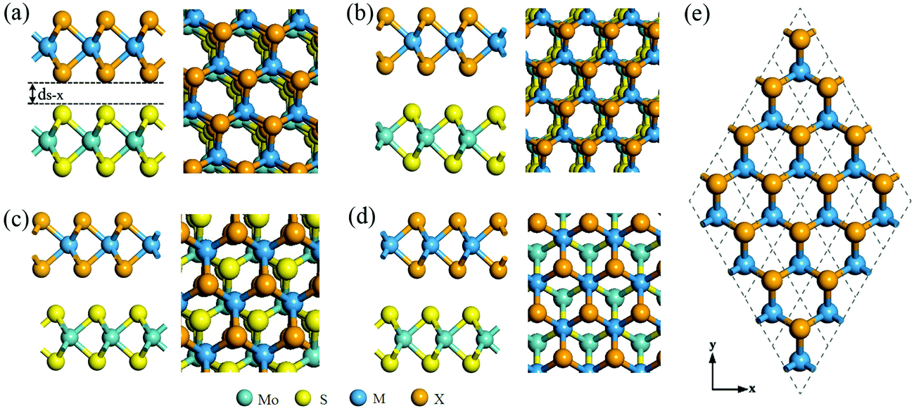 | ||
| Fig. 1 Atomic models of the MX2/MoS2 heterobilayer with four different types of layer-on-layer stacking: (a) AA stacking, (b) C7 stacking, (c) C27 stacking and (d) T stacking. For each stacking configuration, the left and right panels display the side and top views, respectively. The ds−x denotes the interlayer height difference between X (top-layer) and S (lower-layer) atoms. (e) The tensile strain can be applied along x- or/and y-directions. | ||
Results and discussion
1. Heterobilayers of MX2/MoS2
It is known that monolayer MX2 exhibits two possible structures, namely, H or T phase. The H structure is only considered here because it is more stable than T for most of the MX2 structures considered in this study.36 Moreover, following a previous study,17 we consider four different types of bilayer stacking, namely, AA, C7, C27, and T stacking, to describe how a H–MX2 monolayer is superimposed on the 2H–MoS2 monolayer (see Fig. 1). A testing calculation suggests that the electronic structure is more or less the same for the four different stackings, consistent with a previous study.17 Therefore, only the C7 stacking that gives rise to the lowest energy in most heterobilayer systems is reported for the electronic structure calculations. The optimized cell parameters and the vertical height differences between interlayer X and S atoms (ds−x, as shown in Fig. 1(a)) are listed in ESI Table S1.† The ds−x of X and S atoms in different MX2/MoS2 heterobilayers is less than 3.2 Å due to van der Waals interaction between MX2 and MoS2 layers.The computed electronic bandgaps of MX2 monolayers, bilayers, and MX2/MoS2 heterobilayers, as well as the binding energies per unit cell of MX2/MoS2 heterobilayers are listed in Table 1. The binding energies are defined as Eb = E(MX2/MoS2 heterobilayer) − E(MX2 monolayer) − E(MoS2 monolayer), where E(MX2/MoS2 heterobilayer) is the total energy of the MX2/MoS2 heterobilayer and E(MX2 monolayer) is the total energy of the MX2 monolayer. For M = Mo, W, Cr, the MX2 monolayers are direct semiconductors with the conduction band minimum (CBM) and valence band maximum (VBM) being located at the K point (ESI Fig. S1†). However, their corresponding bilayers become indirect semiconductors. For example, the MoS2 monolayer is a direct semiconductor with a computed bandgap of 1.67 eV (PBE), while the bilayer is an indirect semiconductor with a bandgap of 1.25 eV (PBE). As shown in Fig. 2, the VBM of the bilayer structures relocates to the Γ point from the K point (for the monolayer). The partial charge density at the Γ point is contributed from both monolayers, and it exhibits a strong upward shift, overtaking the energy at the K point.14 For MoS2, WS2, CrS2, and CrSe2 bilayers, their CBM is still located at the K point. For MoSe2, the CBM moves to the Λ point (Fig. 2), and the energy at the Λ point is 5 meV below that at the K point. The WSe2 bilayer has a nearly degenerate energy for the two valleys.
| E g1 (eV) | E g2 | E g3 | E b (eV) | |
|---|---|---|---|---|
| MoS2 | 1.67 Direct | 1.25 Indirect | — | — |
| MoSe2 | 1.46 Direct | 1.20 Indirect | 0.74 Indirect | −0.16 |
| WS2 | 1.81 Direct | 1.43 Indirect | 1.16 Indirect | −0.22 |
| WSe2 | 1.55 Direct | 1.38 Indirect | 0.57 Direct | −0.16 |
| CrS2 | 0.93 Direct | 0.68 Indirect | 0.39 Indirect | −0.14 |
| CrSe2 | 0.74 Direct | 0.60 Indirect | 0.69 Indirect | −0.22 |
| FeS2 | Metal | Metal | Metal | −0.31 |
| VS2 | Metal | Metal | Metal | −0.23 |
| VSe2 | Metal | Metal | Metal | −0.16 |
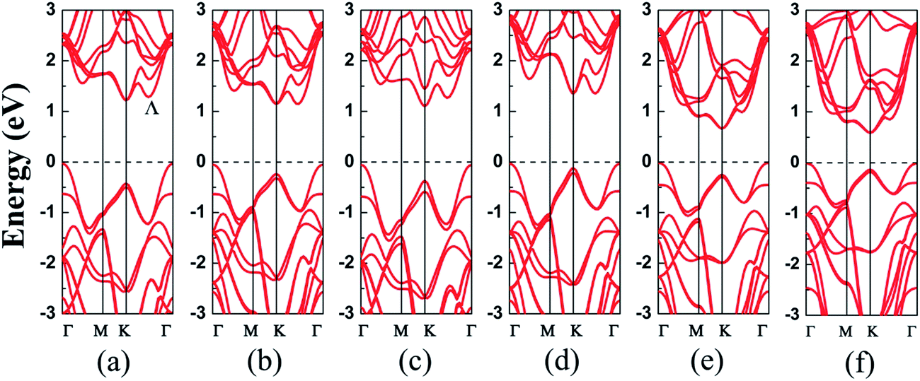 | ||
| Fig. 2 Computed band structures (PBE) of the homogeneous bilayer of (a) MoS2, (b) MoSe2, (c) WS2, (d) WSe2, (e) CrS2, and (f) CrSe2. All bilayers show an indirect bandgap. | ||
As shown in Fig. 3, most MX2/MoS2 heterobilayers are indirect semiconductors, whereas only the WSe2/MoS2 heterobilayer possesses a direct bandgap of 0.57 eV. Different from their own bilayers, the CBM of heterostructures is all located at the K point, while the VBM is located at the Γ point. For the WSe2/MoS2 heterobilayer, however, the VBM is still located at the K point, resulting in a direct-bandgap semiconductor (PBE). The VBM of MoSe2/MoS2 at the Γ point (V1, Fig. 3(a)) shows a mixing of densities from both monolayers. The CBM (C1, Fig. 3(a)) and the valence band edge (PBE, V2, Fig. 3(a)) at the K point are localized for MoSe2 and MoS2, respectively. The CBM and VBM positions of MX2 monolayers are shown in ESI Fig. S2.† One can see that the band structures of WS2/MoS2, WSe2/MoS2, and CrS2/MoS2 are similar to those of MoSe2/MoS2, showing type II alignment of the band edges, which may be of advantageous for the separation of electron–hole pairs.14
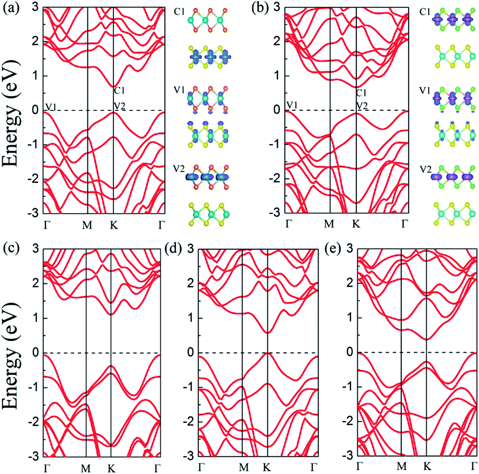 | ||
| Fig. 3 Computed band structures (PBE) and partial charge density of C1, V1, and V2 states of the heterobilayer: (a) MoSe2/MoS2 and (b) CrSe2/MoS2. The isosurface value in (a) and (b) is 0.02 e Å−3. Computed band structures (PBE) of heterobilayer: (c) WS2/MoS2, (d) WSe2/MoS2, and (e) CrS2/MoS2. Only the WSe2/MoS2 heterobilayer exhibits a direct bandgap. | ||
For CrSe2/MoS2, the VBM at the Γ point is over that at the K point by 67 meV (Fig. 3(b)), and the VBM at the Γ point is mainly due to the CrSe2 layer with little contribution from the MoS2 layer. However, different from other heterobilayers, the CBM and VBM at the K point are both due to CrSe2, which exhibit the type I alignment. For MX2 (M = Fe, V), the monolayer, bilayer, and MX2/MoS2 heterobilayers all exhibit metallic character, while the ferromagnetism is still kept by the heterobilayer. As shown in Table 1, the binding energies of all the MX2 and MoS2 heterobilayers are in the range of −0.31 to −0.14 eV, further supporting the weak van der Waals interaction between the MX2 and MoS2 layers.
2. Tunable bandgaps via tensile strain
Strain modulation has been commonly used in low-dimensional systems to tune the electronic structures. For TMD monolayers, the strain-induced bandgap modification has been predicted from recent first-principles calculations.21,22,24 The photoluminescence spectroscopy measurement has further confirmed the strain effect on the electronic structure of both monolayer and bilayer TMD systems. Hence, it is of both fundamental and practical interest to examine the effect of tensile strains on the electronic properties of MX2/MoS2 heterobilayers. As such, first, we have applied in-plane tensile strain by stretching the hexagonal cell biaxially,24 and the biaxial strain is defined as ε = Δa/a0, where a0 is unstrained cell parameters and Δa + a0 is strained cell parameters.As mentioned above, among the heterobilayers considered in this study, only the WSe2/MoS2 heterobilayer exhibits the direct-bandgap character (Fig. 3(d)). Nevertheless, we find that a 1% biaxial strain can turn the heterobilayer into an indirect semiconductor as the VBM is relocated from the K to the Γ point. The latter is 16 meV higher than that of the K point. The CBM is still located at the K point regardless of the strain. As the energy difference between the valence band at the K point and the Γ point is just 100 meV for the unstrained WSe2/MoS2 heterobilayer, the mixing feature of the Γ point renders it more easily affected by the tensile strain. Hence, even a relatively small strain (1%) can result in higher Γ point than the K point in the energy diagram, leading to an indirect bandgap. On further increasing the biaxial strain, the energy difference between the valence band edges at these two points becomes greater. And the indirect bandgap decreases with the biaxial tensile strain, as shown in Fig. 4.
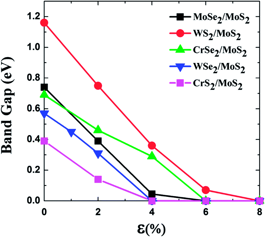 | ||
| Fig. 4 Computed electronic bandgaps (PBE) of MX2/MoS2 (M = Mo, W, Cr) heterobilayers versus the biaxial tensile strain, ranging from 0 to 8%. | ||
The computed electronic bandgaps of the semiconducting MX2/MoS2 (M = Mo, W, Cr; X = S, Se) heterobilayers as a function of the biaxial tensile strain are shown in Fig. 4. For the unstrained MoSe2/MoS2 heterobilayer, it is an indirect semiconductor with a bandgap of 0.74 eV. With the 2% biaxial tensile strain, the bandgap is reduced to 0.39 eV but still indirect. When the tensile strain increases to 4%, the bandgap is further reduced to 0.045 eV. Eventually the MoSe2/MoS2 heterobilayer turns into a metal when the biaxial strain reaches 6%. For the WS2/MoS2 heterobilayer, it turns into a metal when the biaxial tensile strain reaches 8%.
As shown in Fig. 4, the bandgaps of MX2/MoS2 (M = Mo, W, Cr; X = S, Se) generally decrease with the biaxial tensile strain, and undergo a semiconductor-to-metal transition at certain critical strains. To gain more insight into this transition, we have analyzed the band structures and partial density of states (PDOS) of the unstrained and strained MX2/MoS2 heterobilayers. Here, we use the PDOS of the WS2/MoS2 heterobilayer as an example (see Fig. 5). The unstrained WS2/MoS2 heterobilayer is an indirect semiconductor with a bandgap of 1.16 eV. The VBM is mainly contributed by the d orbital of W in the WS2 layer, while the CBM is mainly contributed by the d orbital of Mo in the MoS2 layer. With a 4% biaxial tensile strain, the CBM is shifted toward the Fermi level, resulting in a reduced (indirect) bandgap (0.36 eV) for the WS2/MoS2 heterobilayer. With an 8% biaxial tensile strain, the shift of the CBM leads to the semiconductor-to-metal transition (see the bottom panel of Fig. 5).
 | ||
| Fig. 5 Computed partial density of states (PDOS) of the WS2/MoS2 heterobilayer under 0%, 4%, or 8% biaxial tensile strain. The vertical dashed line represents the Fermi level. | ||
For the semiconducting CrS2/MoS2 heterobilayer, the PBE calculation suggests that it becomes a metal with a 4% biaxial tensile strain. Here, a 2 × 2 supercell is used. Under a 2% biaxial tensile strain the CrS2/MoS2 heterobilayer undergoes a nonmagnetic-to-antiferromagnetic transition. When the biaxial tensile strain increases to 10%, the CrS2/MoS2 heterobilayer turns into a strong antiferromagnetic coupling metal. Bader charge analysis suggests that the charge transfer between CrS2 and MoS2 layers is nearly zero under the 0% strain, and increases to 0.1 e under the 10% strain, indicating that the charge transfer between CrS2 and MoS2 layers increases with increasing tensile strain, leading to spontaneous polarization between CrS2 and MoS2 layers. In stark contrast, the CrS2 monolayer cannot become magnetic even under a tensile strain as high as 15%. These results indicate that the charge transfer between MoS2 and CrS2 layers plays a key role in the nonmagnetic-to-antiferromagnetic transition.
Note also that several metallic heterobilayers MX2/MoS2 (M = Fe, V; X = S, Se) still maintain their metallic character under the biaxial tensile strain. Nevertheless, we find that the magnetic moment of M and X atoms increases with the increase of the biaxial tensile strain from 0% to 10% (see Table 2). A close examination of the PDOS of the VS2/MoS2 heterobilayer with 0%, 4% or 8% biaxial tensile strain (Fig. 6(a)) reveals that the state corresponding to the Fermi level is mainly contributed by d-states of V, which becomes more localized with increasing strain. As shown in Fig. 6(b), the spin charge density of the VS2/MoS2 heterobilayer with a 4% biaxial tensile strain suggests that the magnetism is mainly contributed by the V atom (0.98 μB) while the S atoms of VS2 carry a small magnetic moment of −0.06 μB, consistent with the analysis based on PDOS. As a result, nano-mechanical modulation of strain can turn the nonmagnetic CrS2/MoS2 heterobilayer into antiferromagnetic. The strain can also enhance the spin polarization of the MX2/MoS2 (M = Fe, V; X = S, Se) heterobilayers. This feature may be exploited in spintronic applications such as mechanical nano-switch for spin-polarized transport.
| Strain | FeS2 | VS2 | VSe2 | |||
|---|---|---|---|---|---|---|
| Fe | S | V | S | V | Se | |
| 0% | 1.05 | −0.03 | 0.91 | −0.04 | 1.02 | −0.05 |
| 2% | 1.50 | −0.04 | 0.94 | −0.05 | 1.05 | −0.06 |
| 4% | 1.60 | −0.06 | 0.98 | −0.06 | 1.08 | −0.07 |
| 6% | 1.72 | −0.07 | 1.01 | −0.07 | 1.11 | −0.08 |
| 8% | 1.84 | −0.09 | 1.14 | −0.08 | 1.15 | −0.09 |
| 10% | 1.98 | −0.10 | 1.19 | −0.09 | 1.18 | −0.10 |
 | ||
| Fig. 6 (a) Computed PDOS of the VS2/MoS2 heterobilayer under 0%, 4% or 8% biaxial tensile strain. The vertical dashed line represents the Fermi level. (b) The spin charge density of the VS2/MoS2 heterobilayer with a 4% biaxial tensile strain. The isosurface value is 0.01 e Å−3. The blue indicates the positive values. | ||
Besides biaxial tensile strains, we also investigate effects of a uniaxial tensile strain in either x- or y-direction (Fig. 1(e)). Our calculations suggest that the bandgaps in both cases are reduced with increasing strain, as shown in Fig. 7. As mentioned above, MoSe2 (WS2, CrSe2, CrS2)/MoS2 heterobilayers are indirect semiconductors. Under a uniaxial tensile strain these heterobilayers remain indirect semiconductors, the same behavior as under a biaxial tensile strain. However, the WSe2/MoS2 heterobilayer is predicted to be a direct semiconductor based on the PBE calculation. With a 2% uniaxial tensile strain along either x- or y-direction, the heterobilayer still remains a direct semiconductor, which is very different from that under the biaxial tensile strain for which the heterobilayer becomes an indirect semiconductor under only 1% biaxial tensile strain. When the uniaxial tensile strain increases to 4%, the WSe2/MoS2 heterobilayer turns into an indirect semiconductor.
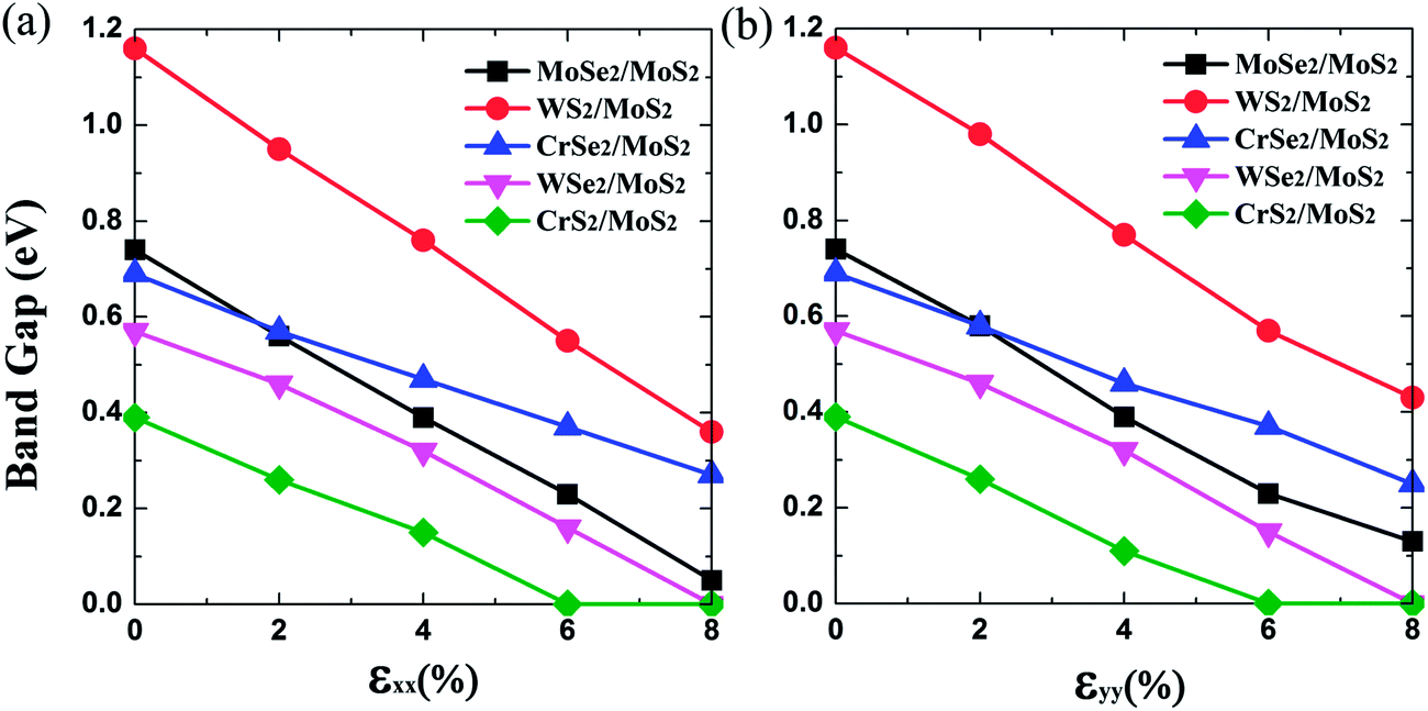 | ||
| Fig. 7 Computed bandgaps of MX2/MoS2 (M = Mo, W, Cr) heterobilayers versus the uniaxial tensile strain in the (a) x- or (b) y-direction, ranging from 0 to 8%. | ||
Since the WSe2/MoS2 heterobilayer is the only system here showing a direct bandgap (Fig. 3(d)), additional PBE calculations including the spin-orbit coupling effects are presented in ESI Fig. S3–S5.† Under either the biaxial or uniaxial tensile strain, the bandgap is still direct but much smaller. Moreover, the direct-to-indirect transition is not seen with increasing strain. Nevertheless, the bandgap still decreases with increasing strain and exhibits a semiconductor-to-metal transition, consistent with the PBE results. Moreover, HSE06 calculations are also performed for the WSe2/MoS2 heterobilayer. Although HSE06 tends to overestimate the bandgap (see ESI Fig. S6† for a test calculation with the bilayer MoS2), the overall trend in bandgap reduction with increasing strain is the same as that predicted from the PBE calculations (see ESI Fig. S3–S5†). However, the direct-to-indirect transition does not occur until 4% biaxial strain (ESI Fig. S3(l)†) or 6% uniaxial strain (ESI Fig. S4 and S5†).
3. External electric field in the normal direction
MX2 (M = Mo, W, Cr; X = S, Se) monolayers are direct-bandgap semiconductors, whereas their homogeneous bilayers are indirect-gap semiconductors. Importantly, among the TMD heterobilayers considered, only the WSe2/MoS2 heterobilayer is a direct-bandgap semiconductor, while the MoSe2/MoS2 heterobilayer possesses a quasi-direct bandgap with only 0.1 eV difference between the direct and indirect bandgap (Fig. 3(a)), consistent with the previous study.15 Note that the HSE06 calculation suggests that the MoSe2/MoS2 heterobilayer is a direct bandgap semiconductor (ESI Fig. S6(b)†). Previous studies also predicted direct-bandgap characters of WS2/WSe2 and MoTe2/MoS2 heterobilayers.14,15 We have computed the dipole moments of WSe2/MoS2 and MoSe2/MoS2 heterobilayers, and found that the dipole moments of both systems are about 0.01 e Å greater than those of the MS2/MoS2 (M = Mo, W, Cr) systems, suggesting that the stronger spontaneous polarization in the MSe2/MoS2 systems is responsible for the underlying direct-bandgap or quasi-direct-bandgap characters. This large difference in spontaneous polarization may stem from the electronegativity difference between S and Se. Assuming this explanation is valid, one could ask if a vertical electric field is applied to the system to increase the spontaneous polarization in MoSe2/MoS2, will the system undergo an indirect-to-direct bandgap transition? Our test calculation shows that the answer to this question is yes. As shown in Fig. 8(b), the applied 0.1 V Å−1 electric field can induce the indirect-to-direct bandgap transition in the MoSe2/MoS2 heterobilayer. Indeed, the VBM is moved from the Γ point to the K point, and the direct transition of K–K is 0.03 eV narrower than the indirect transition of Γ–K. Further increasing the external field will reduce the direct bandgap more significantly than the indirect bandgap (Fig. 8(a)). Results of a Bader charge population analysis are presented in ESI Table S2.† One can see that the charge transfer between the MoS2 and MoSe2 layers indeed increases with the external electric field. We have also examined the bandgaps of the MoSe2/MoS2 heterobilayer with the geometry optimized under different electric fields; the results are nearly the same as those without the geometric optimization under the electric field (see ESI Table S3†).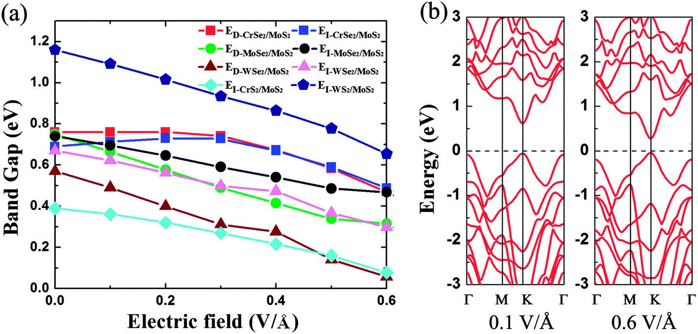 | ||
| Fig. 8 (a) Computed bandgaps (PBE) of MX2/MoS2 (M = Mo, W, Cr; X = S, Se) heterobilayers versus the applied electric field in the normal direction, whose strength varies from 0 to 0.6 V Å−1. ED indicates the direct bandgap of K–K transition, EI indicates the indirect bandgap of Γ–K transition. A crossover of the ED and EI curves for the heterobilayer (MoSe2/MoS2 and CrSe2/MoS2) indicates an indirect-direct bandgap transition. The WSe2/MoS2 heterobilayer is always a direct-bandgap semiconductor for field strength <0.6 V Å−1. (b) Computed band structures of the MoSe2/MoS2 heterobilayer under an electric field of 0.1 V Å−1 or 0.6 V Å−1. | ||
We have also examined the spontaneous polarization in the CrSe2/MoS2 heterobilayer which possesses a dipole moment of 0.005 e Å. Under an external field of 0.5 V Å−1, an indirect-to-direct bandgap transition is predicted. The WSe2/MoS2 heterobilayer always retains the direct-bandgap feature under the external electric field (Fig. 8(a)), and its direct bandgap exhibits a steeper reduction with the increase of external electric field. Finally, although the indirect-to-direct bandgap transition is not observed for WS2/MoS2 and CrS2/MoS2 heterobilayers, their indirect bandgaps exhibit a nearly linear reduction with increase of the electric field. In summary, it appears that the external electric field not only can modify bandgaps of these heterobilayers but also can induce an indirect-to-direct bandgap semiconducting transition beyond a critical field.
Conclusion
We have performed a systematic study of electronic and magnetic properties of MX2/MoS2 (M = Mo, W, Cr, Fe, V; X = S, Se) heterobilayers. Our PBE calculations suggest that MX2/MoS2 (M = Mo, W, Cr; X = S, Se) heterobilayers are indirect-bandgap semiconductors with the exception of the WSe2/MoS2 heterobilayer which can retain the direct-bandgap semiconducting character. Either a vertical electric field or a tensile strain can induce modulation of the bandgaps for these systems. Typically, an increase of the tensile strain decreases the bandgap of heterobilayers. Beyond a critical strain, the semiconductor-to-metal transition may occur. For the WSe2/MoS2 heterobilayer, a direct-to-indirect bandgap transition may occur beyond a critical biaxial or uniaxial strain; however, its bandgap is always direct regardless of the strength of the external electric field (<0.6 V Å−1). Moreover, unusual antiferromagnetism is observed in the CrS2/MoS2 system with a 2% biaxial tensile strain. The magnetic moment of M and X atoms (M = Fe, V; X = S, Se) increases with increase of the biaxial tensile strain for the MX2/MoS2 heterobilayers. The spontaneous polarization in the S/Se interface is more enhanced than the S/S interface. When an electric field is applied in the same direction as the spontaneous polarization, the indirect-to-direct bandgap semiconducting transition can be observed in two heterobilayers (MoSe2/MoS2 and CrSe2/CrS2). These theoretical predictions suggest that TMD heterobilayer materials are very promising for optoelectronic applications due to their tunable bandgaps by applying tensile strain or vertical electric field, possible direct-to-indirect bandgap transition in the WSe2/MoS2 heterobilayer by the strain, and possible indirect-to-direct bandgap transition in MoSe2/MoS2 and CrSe2/CrS2 by the vertical electric field.Acknowledgements
XCZ is grateful to valuable discussions with Professors Ali Adibi, Eric Vogel, Joshua Robinson, and Ali Eftekhar. The USTC group is supported by the National Basic Research Programs of China (nos 2011CB921400 and 2012CB 922001), NSFC (grant nos 21121003, 11004180, and 51172223), One Hundred Person Project of CAS, Strategic Priority Research Program of CAS (XDB01020300), Shanghai Supercomputer Center, and Hefei Supercomputer Center. UNL group is supported by ARL (grant no. W911NF1020099), NSF (grant no. DMR-0820521), and a grant from USTC for (1000plan) Qianren-B summer research and a grant from UNL Nebraska Center for Energy Sciences Research.References
- Y. Li, Z. Zhou, S. Zhang and Z. Chen, J. Am. Chem. Soc., 2008, 130, 16739–16744 CrossRef CAS PubMed.
- K. F. Mak, C. Lee, J. Hone, J. Shan and T. F. Heinz, Phys. Rev. Lett., 2010, 105, 136805 CrossRef.
- A. Splendiani, L. Sun, Y. Zhang, T. Li, J. Kim, C.-Y. Chim, G. Galli and F. Wang, Nano Lett., 2010, 10, 1271–1275 CrossRef CAS PubMed.
- B. Radisavljevic, A. Radenovic, J. Brivio, V. Giacometti and A. Kis, Nat. Nanotechnol., 2011, 6, 147–150 CrossRef CAS PubMed.
- H. Wang, L. L. Yu, Y. H. Lee, Y. M. Shi, A. Hsu, M. L. Chin, L. J. Li, M. Dubey, J. Kong and T. Palacios, Nano Lett., 2012, 12, 4674–4680 CrossRef CAS PubMed.
- B. Radisavljevic, M. B. Whitwick and A. Kis, ACS Nano, 2011, 5, 9934–9938 CrossRef CAS PubMed.
- Y. Yoon, K. Ganapathi and S. Salahuddin, Nano Lett., 2011, 11, 3768–3773 CrossRef CAS PubMed.
- A. Geim and I. Grigorieva, Nature, 2013, 499, 419–425 CrossRef CAS PubMed.
- S. Bertolazzi, D. Krasnozhon and A. Kis, ACS Nano, 2013, 7, 3246–3252 CrossRef CAS PubMed.
- L. Britnell, R. Gorbachev, R. Jalil, B. Belle, F. Schedin, A. Mishchenko, T. Georgiou, M. Katsnelson, L. Eaves and S. Morozov, Science, 2012, 335, 947–950 CrossRef CAS PubMed.
- T. Georgiou, R. Jalil, B. D. Belle, L. Britnell, R. V. Gorbachev, S. V. Morozov, Y.-J. Kim, A. Gholinia, S. J. Haigh and O. Makarovsky, Nat. Nanotechnol., 2012, 8, 100–103 CrossRef PubMed.
- W. J. Yu, Z. Li, H. Zhou, Y. Chen, Y. Wang, Y. Huang and X. Duan, Nat. Mater., 2012, 12, 246–252 CrossRef PubMed.
- J. Kang, J. Li, S.-S. Li, J.-B. Xia and L.-W. Wang, Nano Lett., 2013, 13, 5485–5490 CrossRef CAS PubMed.
- H.-P. Komsa and A. V. Krasheninnikov, Phys. Rev. B: Condens. Matter Mater. Phys., 2013, 88, 085318 CrossRef.
- H. Terrones, F. López-Urías and M. Terrones, Sci. Rep., 2013, 3, 1549 Search PubMed.
- Y. Ma, Y. Dai, M. Guo, C. Niu and B. Huang, Nanoscale, 2011, 3, 3883–3887 RSC.
- K. Kośmider and J. Fernández-Rossier, Phys. Rev. B: Condens. Matter Mater. Phys., 2013, 87, 075451 CrossRef.
- A. Ramasubramaniam, D. Naveh and E. Towe, Phys. Rev. B: Condens. Matter Mater. Phys., 2011, 84, 205325 CrossRef.
- Q. Liu, L. Li, Y. Li, Z. Gao, Z. Chen and J. Lu, J. Phys. Chem. C, 2012, 116, 21556–21562 CAS.
- L. Kou, T. Frauenheim and C. Chen, J. Phys. Chem. Lett., 2013, 4, 1730–1746 CrossRef CAS.
- P. Johari and V. B. Shenoy, ACS Nano, 2012, 6, 5449–5456 CrossRef CAS PubMed.
- Y. Ma, Y. Dai, M. Guo, C. Niu, Y. Zhu and B. Huang, ACS Nano, 2012, 6, 1695–1701 CrossRef CAS PubMed.
- W. S. Yun, S. Han, S. C. Hong, I. G. Kim and J. Lee, Phys. Rev. B: Condens. Matter Mater. Phys., 2012, 85, 033305 CrossRef.
- Y. Zhou, Z. Wang, P. Yang, X. Zu, L. Yang, X. Sun and F. Gao, ACS Nano, 2012, 6, 9727–9736 CrossRef CAS PubMed.
- H. J. Conley, B. Wang, J. I. Ziegler, R. F. Haglund, S. T. Pantelides and K. I. Bolotin, Nano Lett., 2013, 13, 3626–3630 CrossRef CAS PubMed.
- Y. Y. Hui, X. Liu, W. Jie, N. Y. Chan, J. Hao, Y.-T. Hsu, L.-J. Li, W. Guo and S. P. Lau, ACS Nano, 2013, 7, 7126–7131 CrossRef CAS PubMed.
- A. Lu, R. Zhang and S. Lee, Appl. Phys. Lett., 2007, 91, 263107 CrossRef PubMed.
- Z. Zhang and W. Guo, Phys. Rev. B: Condens. Matter Mater. Phys., 2008, 77, 075403 CrossRef.
- C. Zhang, A. De Sarkar and R.-Q. Zhang, J. Phys. Chem. C, 2011, 115, 23682–23687 CAS.
- Z. Zhang, W. Guo and B. I. Yakobson, Nanoscale, 2013, 6381–6387 RSC.
- S. Bhattacharyya and A. K. Singh, Phys. Rev. B: Condens. Matter Mater. Phys., 2012, 86, 075454 CrossRef.
- J. N. Coleman, M. Lotya, A. O’Neill, S. D. Bergin, P. J. King, U. Khan, K. Young, A. Gaucher, S. De and R. J. Smith, Science, 2011, 331, 568–571 CrossRef CAS PubMed.
- J. Feng, X. Sun, C. Wu, L. Peng, C. Lin, S. Hu, J. Yang and Y. Xie, J. Am. Chem. Soc., 2011, 133, 17832–17838 CrossRef CAS PubMed.
- R. J. Smith, P. J. King, M. Lotya, C. Wirtz, U. Khan, S. De, A. O'Neill, G. S. Duesberg, J. C. Grunlan and G. Moriarty, Adv. Mater., 2011, 23, 3944–3948 CrossRef CAS PubMed.
- X. Zhang and Y. Xie, Chem. Soc. Rev., 2013, 42, 8187–8199 RSC.
- C. Ataca, H. Sahin and S. Ciraci, J. Phys. Chem. C, 2012, 116, 8983–8999 CAS.
- H. L. Zhuang and R. G. Hennig, J. Phys. Chem. C, 2013, 117, 20440–20445 CAS.
- G. Kresse and J. Furthmüller, Phys. Rev. B: Condens. Matter Mater. Phys., 1996, 54, 11169 CrossRef CAS.
- G. Kresse and J. Furthmüller, Comput. Mater. Sci., 1996, 6, 15–50 CrossRef CAS.
- G. Kresse and J. Hafner, Phys. Rev. B: Condens. Matter Mater. Phys., 1993, 47, 558 CrossRef CAS.
- G. Kresse and D. Joubert, Phys. Rev. B: Condens. Matter Mater. Phys., 1999, 59, 1758 CrossRef CAS.
- J. P. Perdew, K. Burke and M. Ernzerhof, Phys. Rev. Lett., 1996, 77, 3865 CrossRef CAS.
- J. Klimeš, D. R. Bowler and A. Michaelides, J. Phys.: Condens. Matter, 2010, 22, 022201 CrossRef PubMed.
- J. Klimeš, D. R. Bowler and A. Michaelides, Phys. Rev. B: Condens. Matter Mater. Phys., 2011, 83, 195131 CrossRef.
- J. Neugebauer and M. Scheffler, Phys. Rev. B: Condens. Matter Mater. Phys., 1992, 46, 16067–16080 CrossRef CAS.
- E. Sanville, S. D. Kenny, R. Smith and G. Henkelman, J. Comput. Chem., 2007, 28, 899–908 CrossRef CAS PubMed.
- J. Paier, M. Marsman, K. Hummer, G. Kresse, I. C. Gerber and J. G. Ángyán, J. Chem. Phys., 2006, 125, 249901 CrossRef PubMed.
- Y.-S. Kim, K. Hummer and G. Kresse, Phys. Rev. B: Condens. Matter Mater. Phys., 2009, 80, 035203 CrossRef.
Footnotes |
| † Electronic supplementary information (ESI) available. See DOI: 10.1039/c3nr06072a |
| ‡ Both authors contribute equally to this work. |
| This journal is © The Royal Society of Chemistry 2014 |