 Open Access Article
 This Open Access Article is licensed under a
 Creative Commons Attribution 3.0 Unported Licence
Dispersion and characterization of arc discharge single-walled carbon nanotubes – towards conducting transparent films†
B.
Rösner
a,
D. M.
Guldi
a,
J.
Chen
b,
A. I.
Minett
c and
R. H.
Fink
*a
aDepartment Chemie und Pharmazie, Friedrich-Alexander-Universität Erlangen-Nürnberg (FAU), Egerlandstraße 3, 91058 Erlangen, Germany. E-mail: rainer.fink@fau.de
bIntelligent Polymer Research Institute (IPRI), University of Wollongong, Squires Way, Wollongong, NSW 2522, Australia
cLaboratory for Sustainable Technology, University of Sydney, Sydney, NSW 2006, Australia
First published on 14th January 2014
Abstract
This study addresses a combination of a well-developed and mild dispersion method and high-quality arc discharge single-walled carbon nanotubes (SWCNTs) as starting materials. Thus, we advance in fabrication of transparent, conducting films with extraordinary low material loss during SWCNT processing. The starting material was characterized by means of thermogravimetric analysis, high-resolution transmission electron microscopy and Raman spectroscopy. The quality of the starting material and produced dispersions was evaluated by ultraviolet and visible light absorption spectroscopy and Raman spectroscopy. A transparent conductive film was fabricated by drop-casting, whereas films were obtained with electrical to optical conductivity ratios (σDC/σOp) as high as 2.2, combined with a loss of nanotube material during processing well below 20 wt%. High pressure carbon monoxide conversion (HiPCO) SWCNTs, which are very well described in the literature, were used for comparison.
Introduction
Two decades of research disclosed outstanding mechanical and electrical properties of SWCNTs.1–5 Combined with the high transparency of thin SWCNT films, their high inherent conductivity calls for this extraordinary material to be used in transparent, conducting thin films as, for example, electrode materials.6,7The current industry standard for transparent electrodes is indium tin oxide (ITO), whose use is associated with substantial disadvantages which foster the idea to look for replacements. Quite importantly, high prices and the inherent brittleness of this material render ITO electrodes, on one hand, very expensive and, on the other hand, unsuitable for applications such as flexible electronics, etc.8–11 Myriad attempts have been made to realize suitable substitutes for ITO. Most notable are efforts on metal nanowires, such as copper8 or silver,9 and on metal oxide frameworks.12,13 In parallel, a multitude of techniques and procedures have been explored to fabricate carbon-based nanostructured films. Mostly, SWCNT networks have been in focus,7,10,11 followed by graphene films grown on metal surfaces by chemical vapour deposition (CVD)14,15 and, finally, composite materials containing carbon nanotubes and graphene.16–19
None of the aforementioned led, however, to the needed breakthrough to be implemented as thin transparent, conducting electrodes owing to numerous drawbacks. One of these drawbacks is variation in the quality of SWCNTs, even within different batches of the same synthesis process. The latter is certainly followed by the poor dispersability/solubility of SWCNTs in commonly used media. Here, the major obstacle lies in the vast material loss inherent to most approaches to disperse carbon nanotubes.
What limits the applicability of SWCNTs for industrial use in, for example, electronic devices is after all not the fabrication of high-quality transparent, conducting films but the technical demand and financial expenditures to take SWCNTs from scratch to the final product. Much effort has been made on synthesis, purification, and processing of SWCNTs. Nevertheless, the need for simple and cheap procedures, which ensure high device quality upon waste reduction and economic device fabrication, arises.
This requirement begins with the starting material, considering significant variations in the SWCNT quality. SWCNTs are generated in various purities, lengths, chiralities, diameters, and graphitization grades.4,20 While several methods have been developed to purify SWCNTs to remove by-products – amorphous carbon, fullerenes, and metal particles21,22 – the other properties of SWCNTs strongly depend on the synthetic methods. In the light of the theory of conducting SWCNT networks with the contact resistance mainly determining the conductivity, the tube/bundle diameter and length are most significant.7,23,24 Of crucial importance for the control of these parameters are the synthesis conditions; significant progress towards the synthesis of high quality SWCNTs with distinct properties25–28 has been made in recent years. In general, arc discharge and laser ablation SWCNTs fulfil these conditions better, that is, revealing higher degrees of graphitization and larger diameters than what is commonly found in SWCNTs grown by CVD.20
The poor dispersability and bundling of SWCNTs prompt to the needs of a sophisticated dispersion chemistry as a high exfoliation grade is preferred for thin conducting films.5,7,29 Most commonly, SWCNTs are exfoliated by means of a surfactant-based approach that yields stabilized SWCNT dispersions in either aqueous or organic media.29–32 Widely employed surfactants are sodium dodecylbenzene sulfonate (SDBS), sodium dodecyl sulfate (SDS), lithium dodecyl sulfate (LDS), and sodium cholate (SC).30 Typical organic solvents are N-methyl-pyrrolidone (NMP) and N-cyclohexyl-pyrrolidone (CHP).31 Besides the surfactant and the solvent, which clearly govern the dispersion quality, the technical procedure spanning a wide variety of different parameters has also to be taken into account. A rather successful method to obtain exfoliated SWCNTs includes several cycles of tip sonication, bath sonication, and centrifugation.29–31,33 The sonication steps are imperative to break up SWCNT bundles and to homogenize individualized SWCNTs and smaller bundles throughout the dispersion. Nevertheless, sonication requires careful adjustment to provide the right amount of energy to individualize and disperse SWCNTs without damaging them, i.e., shortening them. As a complement, the centrifugation step serves to remove larger agglomerates, whose dispersions would be semistable and, in turn, would contaminate SWCNT thin films. Ultracentrifugation with g-values well over 40![[thin space (1/6-em)]](https://www.rsc.org/images/entities/char_2009.gif) 000 is frequently reported in the literature.34–38 Notably, centrifugation with these high acceleration forces is unsuitable with respect to scaling up due to substantial materials loss.32 The same problem, yet in another circumstance, applies utilizing the dry-filtering technique which successfully opts for the aforementioned problems that arise upon dispersion but merely collects the small fraction of SWCNTs in the gas phase at the exhaust of a CVD reactor.39,40
000 is frequently reported in the literature.34–38 Notably, centrifugation with these high acceleration forces is unsuitable with respect to scaling up due to substantial materials loss.32 The same problem, yet in another circumstance, applies utilizing the dry-filtering technique which successfully opts for the aforementioned problems that arise upon dispersion but merely collects the small fraction of SWCNTs in the gas phase at the exhaust of a CVD reactor.39,40
In the present work, we explore the relationship between the device quality and efficient processing by a combination of a high quality starting material and advanced dispersion techniques under mild conditions. To this end, we focused in our work on the outstanding arc discharge SWCNTs from Iljin Nanotech, which are well known for the effective production of transparent conducting films.17,33,41 Considering the factors that determine SWCNT dispersions – vide supra – our choice went to a mild method developed by Bergin et al. that skips the ultracentrifugation.34 Based on previous experience,29–31 SDS, SDBS, and SC as well as CHP were chosen as surfactants and solvent, respectively. The key advantage of this method is a reduction of material waste during centrifugation, while affording a high dispersion quality as required for device production. The latter is particularly advantageous, especially when using rather expensive SWCNTs such as arc discharge samples.
To shed first light on the efficiency of our approach using high quality starting materials, transparent conducting films were fabricated and characterized. We drop-cast our dispersions onto glass slides as a simple, reliable, and reproducible technique to evaluate their potential as transparent conductors, whereas the fabrication process has to be optimized in future work. This allows us to correlate the characteristics of our films with benchmarks reported in the literature39,40,42,43 and to assess if our method is suitable as a simple and effective process. Aiming for the optimization of the production process in terms of efficiency, we have to relate the overall mass yield to the film performance. Quite obviously, the resulting ratios (σDC/σOp) can therefore not be simply put on a level with other studies which reach outstanding values at the cost of vast material losses but draw a more realistic picture for the major fraction of the starting material.
To date, most dispersion studies are carried out using HiPCO SWCNTs. It seems conclusive that the overall dispersion might suffer from the lack of comparability if different SWCNTs, especially with different defect densities, are used. It is mainly the surface charge of SWCNTs that influences mutual interactions, that is, between SWCNT surfaces, surfactants, and solvents.44 All experiments were carried out with arc discharge as well as HiPCO SWCNTs to allow comparison of the difference in dispersions and in device performance as a function of SWCNT materials. The starting materials were characterized by Raman spectroscopy, high resolution transmission electron microscopy (HR-TEM), energy-dispersive X-ray spectroscopy (EDS), and thermogravimetric analysis (TGA). In addition, absorption spectroscopy (UV-Vis) and Raman spectroscopy were utilized to qualitatively determine the dispersion grade.
Experimental
Arc discharge synthesized SWCNTs were purchased from Iljin Nanotech Co., LTD. (batch number A-100125-1) and HiPCO SWCNTs were purchased from Carbon Nanotechnology, Inc. (batch number P0341). HiPCO nanotubes were used as purchased. Purification of the arc discharge SWCNTs was conducted in two subsequent steps. In the first step, the SWCNTs were annealed in an air stream at 400 °C for three days. The second step was treatment with 2 M hydrochloric acid at 70 °C for one week. After subsequent filtration and washing with water, the SWCNTs were dried at 350 °C in an air stream. SDS, SDBS and CHP were purchased from Sigma-Aldrich; SC was purchased from Fisher Scientific GmbH and used as received. Millipore water (18.2 MΩ cm−1 at 25 °C) was used for the aqueous solvent systems.Raman spectroscopy (using Horiba Jobin Yvon spectrometers with different laser lines: 532 nm and 633 nm) and TGA (TA instruments TGA Q500, under air, flow rate 90 ml min−1, temperature ramp 5°C min−1) were performed with both the pristine and purified SWCNT material. For the HR-TEM measurements (JEOL JEM-2200FS), pristine SWCNTs were deposited onto hollow carbon TEM grids with the aid of a scalpel blade. This, indeed, destroyed the hollow carbon at some parts of the grid, but provided the possibility of depositing SWCNTs without getting in contact with any solvents. The measurements were conducted in areas with an intact carbon film.
The nanotubes were dispersed by a slightly modified method developed by Bergin et al.34 Stock solutions of SDS, SDBS, and SC in Millipore water with a concentration of 10 mg ml−1, which is well above the critical micelle concentration (CMC) of 2.0–2.9 mg ml−1, 0.73 mg ml−1 and 4–6.5 mg ml−1, respectively,30 were prepared by dissolution of the surfactant and stirring for 30 minutes. 1.0 mg of either HiPCO or arc discharge SWCNTs were carefully weighed into glass vials and 10 ml of a surfactant stock solution or CHP were added. If the SWCNT weight slightly differed from that value, more or less solvent was added in order to adjust the SWCNT initial concentration to ci = 0.1 mg ml−1. The solvent–SWCNT mixture was then sonicated with a pulsed tip sonicator for 15 minutes (pulse duration: 1.0 s on/1.0 s off, power: 500 W, amplitude: 40%), followed by one hour of bath sonication and an additional subsequent tip sonication step using identical parameters as before. During tip sonication, the dispersion was cooled using an ice bath to avoid overheating. This technique is believed to only break the SWCNT bundles and to avoid further damage to SWCNTs.34 After sonication, the dispersion was mildly centrifuged for 90 min (3000 g) to remove agglomerates. The supernatant was carefully transferred into a clean vial after centrifugation and stored under ambient conditions.
UV-Vis and near infrared (UV-Vis/NIR) absorption spectra were recorded using a Shimadzu UV-3600 spectrometer. The dispersions were diluted by a factor of ten to reduce absorption saturation. Raman spectra of the processed SWCNTs were recorded on dried droplets of undiluted dispersions. Direct measurements of the wet dispersions proved to be difficult, because the laser spot did not stay in focus due to dynamic effects of the liquid. Raman spectra were generally recorded using a 300 mm−1 grating. The RBM areas were typically recorded with a higher resolution (1800 mm−1 grating). For calibration, the 520.7 cm−1 line of SiO2 was used.
After characterization of the different dispersions, transparent conducting films were fabricated by drop-casting. A droplet of 0.5 ml SWCNT dispersion in CHP was deposited onto a clean glass slide. Prior to deposition, the glass slides were degreased by sonication in fairy liquid solution for 30 minutes, followed by bath sonication in acetone for 30 minutes. The air dried slides were then terminated by immersion into a 10 wt% solution of trimethylsilyl chloride (from Sigma-Aldrich) in Millipore water and a lacing of hydrochloric acid overnight to improve wettability in regard to the solvent CHP. The slides were rinsed with Millipore water and air dried. The dispersion droplet was then deposited onto the slides on a hotplate at around 110 to 120 °C to dry off the solvent. The drying temperature is important as CHP has a high boiling point above 150 °C but decomposes already below that temperature. The dried SWCNT films were then immersed into 12 M nitric acid for 30 minutes to improve the film conductivity.41 The prepared SWCNT films were characterized by UV-Vis spectroscopy in transmission mode and four-point probe sheet resistance measurements (Jandel in-line four-point probe). The sheet resistance was determined at ten different spots within the films, which had around one square centimetre in size, and averaged with a statistical error.
Results and discussion
The properties of HiPCO SWCNTs have been comprehensively described.4,45,46 In stark contrast, properties of arc discharge SWCNTs are barely documented in scientific publications at the moment. Here, we present a full-fledged investigation regarding the properties of Iljin arc discharge SWCNTs.We performed thermogravimetric analyses under air to obtain first estimates on the purity of the starting material. This technique is particularly suited to reveal the graphitization grade of SWCNTs by comparing the maxima of the first derivatives and the amount of residual metal particles. Fig. 1 shows the TGA of arc discharge SWCNTs as received and after two subsequent purification steps in comparison with the TGA of HiPCO SWCNTs.
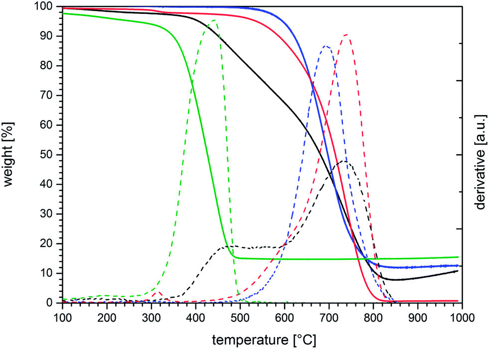 | ||
| Fig. 1 TGA of Iljin SWCNTs – as received/pristine (black), annealed (blue), and acid-treated (red) – and pristine HIPCO SWCNTs (green), performed in air. The continuous graphs depict the relative weight in percentage; the dotted lines represent their first derivatives. | ||
In the case of HiPCO SWCNTs, the entire mass loss stretched from 300–500 °C featuring a maximum of the derivative at about 440 °C. Notably, the graphitization grade of HiPCO SWCNTs tends to be relatively low and the defect density is relatively high. From the latter, a poor thermal stability and a burn-off peak evolve under air at rather low temperatures compared to well graphitized SWCNTs. The defect density does, however, not necessarily scale linearly with the burn-off temperature. For example, a small change in defect density may result in a significantly higher or lower derivative maximum.47 The residue left after annealing to around 500 °C is 14.7 wt%, which was identified in good accordance with the product data sheet46 as an iron catalyst in EDS measurements (see ESI, Fig. S1†).
From the TGA of the arc discharge SWCNTs, a different picture about the sample quality is concluded. We expected that the burn-off temperature is remarkably higher than in HiPCO SWCNTs due to a higher graphitization grade. Roughly 60 wt% of the sample lived up to these expectations with a derivative maximum at 730 °C (Fig. 1). As such, we believe that our batch of arc discharge SWCNTs consists of high-quality, well graphitized SWCNTs with very high thermal stability that is rarely reported in the literature. However, a fraction of about 30 wt% starts to burn off at around 400 °C. In other words, one third of the pristine arc discharge SWCNTs purchased from Iljin Nanotech is a poorer graphitized material – either in the form of CNTs with lower quality or carbon shells around the remaining catalyst particles.48 Amorphous carbon should burn off at temperatures below 400 °C,47 leading to the hypothesis that the shoulder in the TGA stems from some forms of graphitized carbon. The full width at half maximum (FWHM) is also larger than in HiPCO SWCNTs. This seems to be intuitive taking into account that the reaction environment is more uniform during thermal CVD growth than in an arc discharge reactor.
In the context of producing high-quality electronic devices, the existence of one third of a low-quality material is, of course, far from being satisfactory. To further purify the Iljin SWCNTs, the starting material was annealed under air stream at 400 °C for three days. These conditions were carefully chosen based on the TGA of the untreated material and a study reported by Jeong et al.49 On the one hand, the poorly graphitized material starts to burn off at roughly 370 °C while, on the other hand, oxidation of high quality SWCNTs does not set in at these temperatures.
After annealing, the shoulder vanished in line with the expectation. The overall weight of the annealed tubes was reduced by one third and the TGA featured one uniform peak in the first derivative with a maximum around 690 °C. The catalyst residue was with 11.7 wt% higher than in the measurements with the starting material with a value of 7.76 wt%. The higher content of oxidized catalyst particles explains the slightly lower peak temperature due to heating effects located at the metal oxide particles accelerating the oxidation of the surrounding SWCNTs.47 The nature of the catalyst was again revealed by EDS (see Fig. S2†) and was found to be a mixture of iron, cobalt and nickel.
Next, the second purification step was meant to remove metallic impurities. A number of fairly successful methods have been established, including high temperatures, reflux, and treatment with concentrated acids.21 Regardless of the aforementioned, we opted for a method as mild as possible to successfully remove metal particles from the SWCNT material. In particular, the pre-annealed SWCNTs were therefore added to 2 M hydrochloric acid and stirred at 70 °C for one week. The outcome of this treatment is indicated in the TGA plots. Now, the residue is found to be as low as 0.63 wt% and the peak maximum is noted at 738 °C. On the downside, a small shoulder is discernible between 550 and 650 °C. The latter indicates that some SWCNTs have been slightly damaged during the acid treatment as the TGA of the annealed SWCNTs lacks this feature. We attribute this effect to be more than compensated by the purity of the SWCNTs with respect to metal particles. It is worth mentioning that the small peak around 300 °C is related to the presence of the incorporated HCl. Taking the aforementioned into account, a satisfying SWCNT quality with respect to purity was achieved after two mild purification steps.
In terms of a conductive network with the bottleneck for charge transport being junctions between the individual nanotubes, the major impact on the film resistivity stems from the diameter and length of the SWCNTs, or SWCNT bundles, respectively.23,24 Typically, the diameters of HiPCO SWCNTs range from 0.8 to 1.2 nm,46 and their typical lengths range from 0.1 μm to 1 μm. For Iljin SWCNTs, diameters between 1.2 and 1.8 nm with a mean diameter of 1.6 nm are derived from STM and AFM assays with surfactant-stabilized SWCNTs in aqueous media.23 The lengths of these nanotubes attain values between 1 μm and 10 μm.50 When we investigated dispersed Iljin SWCNTs (from an SDBS dispersion with a CNT concentration of approx. 10−3 mg ml−1), typical lengths of small bundles and individual tubes were found between 0.4 μm and 2 μm. Of course, one obvious question arises whether the surfactants tend to contribute to the overall diameters.
In the light of the aforementioned, we conducted a HR-TEM study with particular emphasis on evaluating the SWCNT morphology and deriving their mean diameters. While SWCNTs are generally bundled, which are discernible in TEM, single individual SWCNTs are sometimes seen to stick out from the bundles. Fig. 2 shows representative TEM micrographs taken for Iljin SWCNTs. In line with the expectation, bundles, metal particles as catalyst residues, and some individual SWCNTs are visualized. The metal particles tend to be embedded within carbon shells, which is related to the overall SWCNT growth. In addition, the presence of empty carbon shells correlates with the initial purity featuring a metal content of under 8 wt% as arc discharge reactors are usually loaded with a higher catalyst to carbon ratio.20 The encapsulated metal particles and empty carbon shells are first indications for the existence of carbonic impurities within SWCNT samples. Notably, the latter burn off at far lower temperatures than the average high quality SWCNTs. It seems, however, to be unlikely that their carbonic impurities contribute much to the overall weight – vide supra.
 | ||
| Fig. 2 HR-TEM micrographs of pristine Iljin SWCNTs with magnifications of 8k (a), 50k (b), 100k (c), and 300k (d), recorded using an acceleration voltage of 300 kV. | ||
More important is the SWCNT characterization with respect to their mean diameter. In order to gain first insights, we analysed the diameter of 14 different SWCNTs yielding an average diameter of 1.59 nm and diameters that range from 1.4 to 1.8 nm. This diameter distribution is plausible, when comparing it with the study reported by Nirmalraj et al.,23 apart from the fact that we found no evidence for diameters as small as 1.2 nm.
With the diameters in hands – HiPCO from the data sheet and Iljin SWCNTs from our HR-TEM analysis – we interpreted the UV-Vis/NIR and Raman spectra. To this end, the calculated correlation between SWCNT diameters and energy gaps,51 well known as the Kataura plot, is crucial. On one hand, it enables assigning the observed peaks either to semiconducting or to metallic transitions. On the other hand, it enables determining what kind of SWCNTs are resonant at certain Raman laser lines and, in turn, deriving an estimate about the chirality distribution of the SWCNT samples from the Raman radial breathing mode (RBM).
The UV-Vis/NIR spectra of three different HiPCO SWCNT dispersions (diluted by a factor of ten) are shown in Fig. 3a. Obviously, each of the three different conditions, that is, SDS in water, SC in water, and CHP, is capable of successfully dispersing HiPCO SWCNTs. The spectra imply, especially the good resolution of the van Hove singularities, a fairly high exfoliation of the HiPCO SWCNTs within the dispersions.37 Additionally, the absorption peaks are clearly correlated with the nature of the electronic transition by referring to the SWCNT diameter (see the Kataura plot51). The S11 transitions dominate the range between 900 and 1350 nm, while the S22 transitions evolve between 500 and 850 nm. Finally, the M11 transitions are located between 400 and 650 nm. Thus, all of the transitions are in good accordance with the diameter distribution from 0.8 to 1.2 nm. It is worth mentioning that the M11 transitions overlap partially with the S22 transitions due to the small SWCNT diameters.
 | ||
| Fig. 3 (a) UV-Vis/NIR spectra of pristine HiPCO SWCNT dispersions and (b) pristine Iljin SWCNT dispersions. (see ESI, Fig. S3 and S4† for extended spectra to 2100 nm of solvent and Iljin SWCNT dispersions, including the S11 transitions.) | ||
Notably, the organic dispersions feature broader peaks than the surfactant-stabilized aqueous dispersions. Especially the absorption peaks in the 950 to 1200 nm range are appreciably better resolved in the spectra taken for the SDS and SC dispersions. It has to be noted that the aqueous dispersions were prepared well above the CMC30 to obtain the best exfoliation possible. Still, with CHP to act as a surfactant and a solvent at concentrations high enough to physisorb at the SWCNTs' surface, we anticipated better resolved van Hove singularities. Especially the red-shifted S11 transitions between 900 and 1350 nm indicate larger mean bundle sizes than what is the case for the aqueous dispersions.37 This might be surprising at the first glance considering the high maximum HiPCO SWCNT concentration of 3.5 mg ml−1 that has been reported by Bergin et al. in CHP.31 A possible explanation for the poorer exfoliation grade is related to the higher viscosity of CHP52 relative to the surfactant solutions.53 As such, the removal of SWCNT aggregates and larger SWCNT bundles using the same centrifugation parameters is less efficient. The viscosity effect might also influence the sonication process with respect to the dynamics of solvent molecules physiosorbing at the individual SWCNT surface.
Fig. 3b shows the UV-Vis/NIR spectra for Iljin SWCNTs dispersed in CHP as well as dispersions of SDBS and SC – diluted by a factor of ten. The larger tube diameter shifts the electronic transitions to lower energies with S22 transitions between 850 and 1150 nm, M11 transitions between 600 and 800 nm, and S33 transitions between 400 and 600 nm. With the different transition types not overlapping due to the tube diameters, the energy gaps feature smaller differences. The latter results in a poor resolution of the van Hove singularities, namely the S22 and the M11 transitions. However, this trend is not necessarily due to a poorer exfoliation, but must stem from smaller energetic differences between the individual absorption peaks.
The three dispersions give rise to similar behaviour even at comparable concentrations. Of course, it is extremely difficult to estimate absolute concentrations considering the fact that Iljin SWCNTs differ in type relative to HiPCO SWCNTs. And, as such, they behave differently and feature different absorption coefficients. In high concentration experiments this exerts strong impact. In particular, a concentration of 1.0 mg ml−1 HiPCO SWCNTs was stable in CHP, while dispersions with the same initial concentration of Iljin SWCNTs precipitated after centrifugation. Here, the resulting supernatant has a concentration of roughly 0.2–0.3 mg ml−1. This, in turn, is less than one tenth of the maximum concentration of HiPCO SWCNTs in CHP.31 A higher defect density in HiPCO SWCNTs leads to higher charged surfaces and, per se, to stronger interactions with the surfactants or solvent molecules.44 In other words, these higher defected SWCNTs interact stronger with CHP than less defected and better graphitized Iljin SWCNTs. No doubt, further investigation is necessary, especially to quantify the aforementioned effects and to fully adapt our mild dispersion method, which was developed for dispersing HiPCO SWCNTs, to Iljin arc discharge SWCNTs.
With respect to the overall efficiency of the dispersion process, it is indispensable to evaluate the material loss of Iljin SWCNTs upon dispersion. Hence, absorption spectra were recorded prior and after centrifugation (see ESI, Fig. S5† for the respective absorption spectra). Comparing the absorption yields of the centrifuged dispersions in the range of 88 to 98% of the initial absorptions. These data need to be considered carefully as the absorption coefficients slightly differ prior and after centrifugation. In other words, the mass loss is underestimated.30 Thus, the exact mass loss detection turns out to be highly uncertain, but is, nevertheless, far below 20 wt%.
When turning to Raman analysis of HiPCO SWCNTs and Iljin SWCNTs, the corresponding spectra are shown in Fig. 4. Typical Raman features54 including RBMs as well as D-, G-, G′-, and M-bands are all noted. In addition, iTOLA second order modes are detected. The former four are most characteristic for different SWCNTs and as used to gain insights into the nature of SWCNTs such as chirality distribution, exfoliation grade, and defect density. For example, the chirality distribution is derivable from the RBMs at different excitation energies. The exfoliation grade, on the contrary, evolves as a function of the RBM resolution. Finally, an estimate of the defect density is typically made from the ratio of G- to D-band and/or of G′- to G-band.54
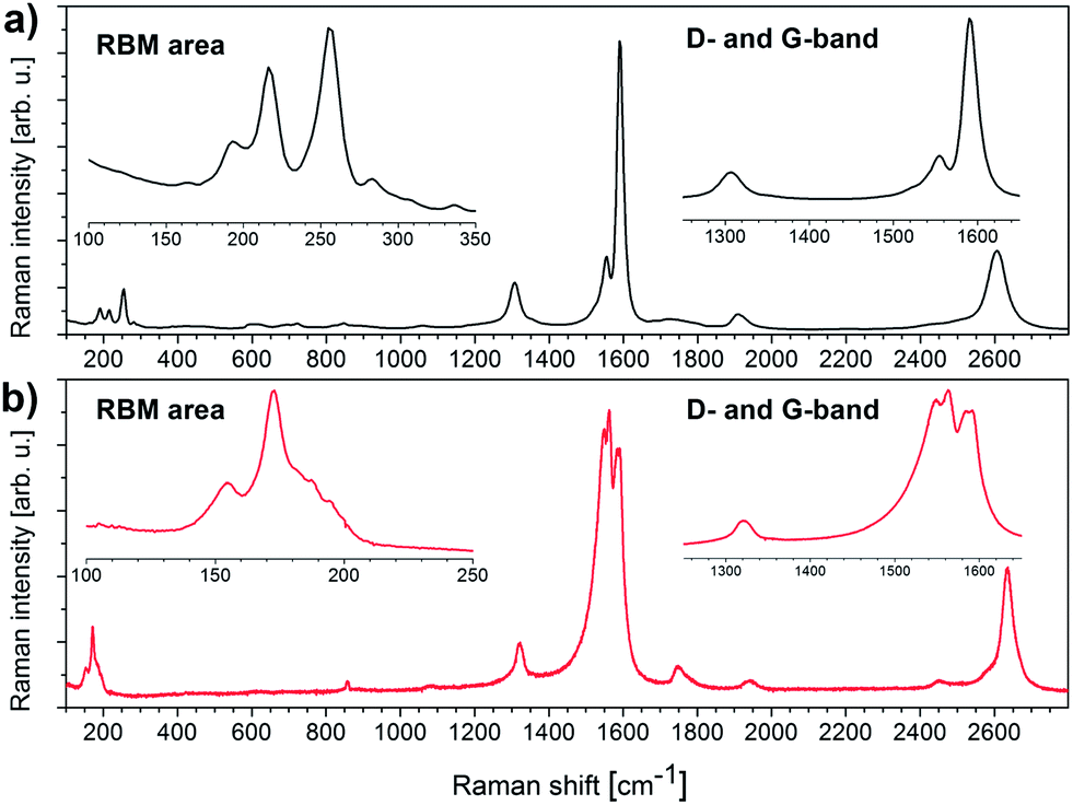 | ||
| Fig. 4 (a) Raman spectra of HiPCO SWCNTs (black) and (b) Iljin SWCNTs (red), excited with a 1.96 eV laser (633 nm). Insets enlarge the radial breathing modes and the D- and G-bands. | ||
The Raman spectrum of HiPCO SWCNTs (see Fig. 4a) confirms the presence of semiconducting species as anticipated from the Kataura plot.51 From the typical line shapes of the G- and the M-band as well as the iTOLA second order mode we conclude that different chiralities are resonantly enhanced at 633 nm and these consist of semiconducting SWCNTs. In the RBM area, clearly resolved features evolve between 150 and 300 cm−1. This is due to the fact that 633 nm excites a relatively large diameter variance and that a good exfoliation grade is realized. The D/G-ratio is, however, rather large, with a peak maximum of the D-band close to that of the G−-band. This finding is in sound agreement with the high defect density disclosed by TGA.
The interpretation of the Iljin SWCNT Raman spectra is less straightforward. A closer look at the Kataura plot shows that there are two electronically different types of SWCNTs, which are in resonance at the 633 nm excitation. Specifically, metallic SWCNTs, with diameters between 1.2 and 1.4 nm, feature their M11 transitions in this energy range, and semiconducting SWCNTs, whose diameters range from 1.6 to 1.8 nm give rise to S33 transitions at around 1.96 eV. As a matter of fact, the observed spectrum is most likely a superposition of Raman features stemming from metallic and semiconducting SWCNTs. It is important to keep this fact in mind as it is helpful for the interpretation of some experimental observations, which seem, at the first glance, to be contradictive.
The resulting Raman spectra show several interesting trends that should be rationalized in the presence of metallic and semiconducting SWCNTs. First of all, the RBMs are shifted to lower wavenumbers relative to what has been seen for HiPCO SWCNTs, namely between 140 and 220 cm−1, and are less well resolved. The aforementioned is due to larger SWCNT diameters, and to a smaller diameter variance of the CNTs that are in resonance at 633 nm.51
The peak at around 150 cm−1 is assigned to semiconducting SWCNTs with a diameter in the range from 1.6 to 1.8 nm and the peak at around 170 cm−1 including its shoulders is assigned to metallic SWCNTs with smaller diameters, that is, from 1.2 to 1.4 nm. It might occur that the peak around 150 cm−1 is rather unusual for semiconducting SWCNTs in terms of the intensity and peak shape relative to the other features. A similar rationale implies the fact that the RBM intensity varies markedly between metallic and semiconducting SWCNTs54 and that the mixture gives rise to a lower variances in RBM vibration energies at larger diameters than at smaller diameters.
Even more striking is the G-band, which appears to be split into four peaks. The nature of this feature proves to be even more complicated to explain. In general, the G-band consists of several overlapping peaks, including coupled vibration modes besides the G+- and the G−-bands. Additionally, the G-mode frequency and the line shape differ rather strongly for semiconducting and metallic SWCNTs.54–56 As we are dealing with Iljin SWCNTs that are resonantly enhanced at 633 nm, the assumption of a mixed semiconducting/metallic resonance is again valid. Bearing this in mind, the two peaks at 1548 and 1563 cm−1 represent the G−-band of metallic and semiconducting SWCNTs, respectively, while the two peaks at 1584 and 1592 cm−1 are related to the G+-band.55 The D- to G-band ratio is remarkably small and the G′- to G-band ratio is much higher than seen for HiPCO SWCNTs – vide supra. From the latter we conclude that the Iljin SWCNTs are low in defects, which is again in good accordance with the TGA results.
Nevertheless, an important question about the tip sonication induced SWCNT damage remains. Fig. 5 shows Raman spectra of Iljin SWCNTs that were recorded for pristine and untreated material as well as a dried film of a CHP dispersion at two different excitation wavelengths. Note that the intensity has been adjusted to the G-bands of both spectra. The comparison discloses after dispersion a slight increase of the D-band intensity and a slight decrease of the G′-band intensity, all relative to the G-band. After all, dispersions of the pre-treated SWCNTs are indeed more defected than the corresponding starting materials. However, the overall differences should be regarded as small at the larger scale, especially considering the subsequent treatment with concentrated nitric acid during film production as the most important step to improve the network conductivity.24
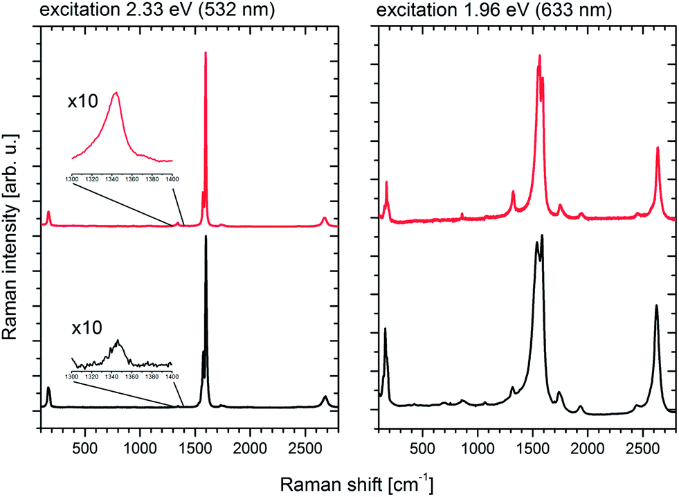 | ||
| Fig. 5 Raman spectra of Iljin SWCNTs before dispersion (as received – black) and after the dispersion procedure (red) at two different excitation energies. | ||
Finally, we correlated the optical transparency with film conductivity to evaluate the potential of SWCNT films deposited from mildly processed dispersions as transparent conductors. It turned out that the transparency varied strongly using exactly the same deposition procedure. The only variable in these experiments was the coverage area on the glass substrates. With the overall variance in hand, we screened the film performance throughout a transparency range at 550 nm from 65 to 86%. The uniformity of the fabricated films lags behind alternative deposition methods, such as filtering. This effect was taken into account by measuring the sheet resistance at ten different locations throughout the entire film and determining statistical errors. Fig. 6 shows the correlation of the sheet resistance with the transparency at 550 nm. We calculated the ratio σDC/σOp, which is a widely used figure of merit,16 to be 2.1 to 2.2 for films produced with Iljin SWCNTs which is an order of magnitude higher than the values we found for HiPCO SWCNT films deposited with the same method. In terms of the theory of conducting networks, the reason for that factor is, besides the higher graphitization grade, mainly the increased length of the arc discharge carbon nanotubes in comparison with HiPCO SWCNTs.57 This performance is, of course, an unsatisfying value in the context of high performance applications. Recently, a new benchmark implies a factor that is 30 times.42 However, we have to emphasize that other studies, which achieve higher performances, process SWCNTs with substantial material loss upon dispersion. For instance, ultracentrifugation to disperse the same kind of nanotubes used by Lee et al.41 with a ratio σDC/σOp of 22.8 induces high material losses of more than 90% by mass.32 Collecting SWCNTs out of the gas phase at the exhaust of a CVD reactor by dry filtering succeeds in forming freestanding films with an electrical to optical conductivity ratio of 41.5, albeit most probably utilizing only a small fraction of starting materials and, finally, dispersion of SWCNTs in chlorosulfonic acid resulted in the highest figure of merit (σDC/σOp = 64.3) reported so far42 but is probably not the most suitable method for a large-scale production compared to the use of organic solvents to deposit SWCNT networks. These facts hamper just levelling up values for resistivity and transparency without considering the impact of the processing method on the overall efficiency. Keeping in mind an SWCNT yield of notably more than 80 wt%, σDC/σOp ratios of 2.1 to 2.2 are in the order of magnitude to become interesting for applications that depend on cheap and reliable transparent conductors.
 | ||
| Fig. 6 Correlation of the sheet resistance and transparency of the SWCNT films. The σDC/σOp ratios are indicated with the red graphs, and values for SWCNT films from ref. 40–42 are shown in the lower right corner for comparison. | ||
Conclusions
A comprehensive study was carried out to evaluate and compare the properties of HiPCO and Iljin SWCNTs in terms of the quality of the starting materials and of dispersions for the production of transparent conducting films. Characterization was done by means of thermogravimetric analysis, high resolution transmission electron microscopy, visible and infrared light absorption spectroscopy, and Raman spectroscopy. This widely diverse set of spectroscopic techniques shed light on the characteristics and the behaviour of different SWCNTs on two accounts. On one hand, it considers a certain point of view or a certain stage of production, as quite common in the literature. On the other hand, it reflects the entire procedure, beginning with the starting material and ending with the deposited films.It was found that the chosen SWCNTs, namely arc discharged SWCNTs from Iljin Nanotech, featured a much higher quality of the starting material than the cheaper and widely used HiPCO SWCNTs. However, purification proved to be necessary utilizing even this material in order to meet high quality requirements. We showed that this material was able to form transparent conducting films with performances resulting in a figure of merit, which is by an order of magnitude higher than HiPCO SWCNT films produced by the same procedure.
It is essential for the ability to industrially produce thin conducting films for applications as transparent electrodes that the production process is cheap, scalable, and straightforward. SWCNT films are thereby predestinated especially for use in flexible devices.58 We demonstrated that the combination of high quality SWCNTs with an optimized dispersion procedure is applicable for the production of transparent conducting SWCNT films of high quality. The key advantage inherent to our method is the extremely low material loss, which is usually the major drawback coming along with most of the other dispersion methods. If this mild method is adapted to disperse high quality starting materials, the film performance will improve significantly compared to low quality nanotubes. Still lagging behind the current benchmark,42 our approach provides a sound basis for further developments, that is, more sophisticated film deposition methods, well developed doping procedures, and starting materials with even higher quality. The effective processing in terms of the amount of starting materials that remains usable for the final application provides optimum preconditions for an industrially worthwhile production of transparent conducting films for – at this stage of the development – at least low performance applications, such as e-paper.
Acknowledgements
We gratefully acknowledge R. Jalili and R. Schäfer for their contributions to this work. We furthermore thank the groups of P. Müller (Department of Physics, FAU), K. Meyer (Chair of Inorganic Chemistry II, FAU) and A. Hirsch (Institute of Advanced Materials and Processes, Fürth, Germany) for technical support. The HR-TEM measurements were performed by D. Mitchell at the Australian Microscopy & Microanalysis Research Facility (University of Sydney). The work was funded by an Australian Research Council Program grant (DP0877348), the Bavarian initiative “Solar Technologies Go Hybrid” and by the DAAD by the ISAP program (50 7300 75).Notes and references
- S. Iijima, Nature, 1991, 354, 56–58 CrossRef CAS
.
- S. J. Tans, M. H. Devoret, H. Dai, A. Thess, R. E. Smalley, L. J. Geerligs and C. Dekker, Nature, 1997, 386, 474–477 CrossRef CAS
- V. Sgobba and D. M. Guldi, Chem. Soc. Rev., 2009, 38, 165–184 RSC
-
M. S. Dresselhaus, G. Dresselhaus and P. Avouris, Carbon Nanotubes: Synthesis, Structure, Properties and Applications, Springer Verlag, Berlin/Heidelberg (Germany), 2001 Search PubMed
- R. H. Baughman, A. A. Zakhidov and W. A. d. Heer, Science, 2002, 297, 787–792 CrossRef CAS PubMed
- Z. Wu, Z. Chen, X. Du, J. M. Logan, J. Sippel, M. Nikolou, K. Kamaras, J. R. Reynolds, D. B. Tanner, A. F. Hebard and A. G. Rinzler, Science, 2004, 305, 1273–1276 CrossRef CAS PubMed
- G. Grüner, J. Mater. Chem., 2006, 16, 3533–3539 RSC
- A. R. Rathmell, S. M. Bergin, Y.-L. Hua, Z.-Y. Li and B. J. Wiley, Adv. Mater., 2010, 22, 3558–3563 CrossRef CAS PubMed
- S. De, T. M. Higgins, P. E. Lyons, E. M. Doherty, P. N. Nirmalraj, W. J. Blau, J. J. Boland and J. N. Coleman, ACS Nano, 2009, 3, 1767–1774 CrossRef CAS PubMed
- V. Scardaci, R. Coull and J. N. Coleman, Appl. Phys. Lett., 2010, 97, 023114 CrossRef PubMed
- V. Sgobba and D. M. Guldi, J. Mater. Chem., 2008, 18, 153–157 RSC
- J. Muster, G. T. Kim, V. Krstic, J. G. Park, Y. W. Park, S. Roth and M. Burghard, Adv. Mater., 2000, 12, 420–424 CrossRef CAS
- C. Streb, R. Tsunashima, D. A. MacLaren, T. McGlone, T. Akutagawa, T. Nakamura, A. Scandurra, B. Pignataro, N. Gadegaard and L. Cronin, Angew. Chem., Int. Ed., 2009, 48, 6490–6493 CrossRef CAS PubMed
- X. Li, W. Cai, S. Kim, J. Nah, D. Yang, R. Piner, A. Velamakanni, I. Jung, E. Tutuc, S. K. Banerjee, J. Colombo and R. S. Ruoff, Science, 2009, 324, 1312–1314 CrossRef CAS PubMed
- S. Bae, H. Kim, Y. Lee, X. Xu, J.-S. Park, Y. Zheng, J. Balakrishnan, T. Lei, H. R. Kim, Y. I. Song, Y.-J. Kim, K. S. Kim, B. Özyilmaz, J.-H. Ahn, B. H. Hong and S. Iijima, Nat. Nanotechnol., 2010, 5, 574–578 CrossRef CAS PubMed
- P. J. King, U. Khan, M. Lotya, S. De and J. N. Coleman, ACS Nano, 2010, 4, 4238–4246 CrossRef CAS PubMed
- S. De, P. E. Lyons, S. Sorel, E. M. Doherty, P. J. King, W. J. Blau, P. N. Nirmalraj, J. J. Boland, V. Scardaci, J. Joimel and J. N. Coleman, ACS Nano, 2009, 3, 714–720 CrossRef CAS PubMed
- U. Dettlaff-Weglikowska, M. Kaempgen, B. Hornbostel, V. Skakalova, J. Wang, J. Liang and S. Roth, Phys. Status Solidi B, 2006, 243, 3440–3444 CrossRef CAS
- T. Mustonen, K. Kordás, S. Saukko, G. Tóth, J. S. Penttilä, P. Heilstö, H. Seppä and H. Jantunen, Phys. Status Solidi B, 2007, 244, 4336–4340 CrossRef CAS
-
M. Meyyappan, Carbon Nanotubes: Science and Applications, CRC Press, Boca Raton (USA)/London (UK)/New York/Washington (USA), 2005 Search PubMed
- I. W. Chiang, B. E. Brinson, R. E. Smalley, J. L. Margrave and R. H. Hauge, J. Phys. Chem. B, 2001, 105, 1157–1161 CrossRef CAS
- T.-J. Park, S. Banerjee, T. Hemraj-Benny and S. S. Wong, J. Mater. Chem., 2006, 16, 141–154 RSC
- P. N. Nirmalraj, P. E. Lyons, S. De, J. N. Coleman and J. J. Boland, Nano Lett., 2009, 9, 3890–3895 CrossRef CAS PubMed
- A. Znidarsic, A. Kaskela, P. Laiho, M. Gaberscek, Y. Ohno, A. G. Nasibulin, E. I. Kauppinen and A. Hassanien, J. Phys. Chem. C, 2013, 117, 13324–13330 CAS
- S. M. Bachilo, L. Balzano, J. E. Herrera, F. Pompeo, D. E. Resasco and R. B. Weisman, J. Am. Chem. Soc., 2003, 125, 11186–11187 CrossRef CAS PubMed
- X. Li, X. Tu, S. Zaric, K. Welsher, W. S. Seo, W. Zhao and H. Dai, J. Am. Chem. Soc., 2007, 129, 15770–15771 CrossRef CAS PubMed
- A. R. Harutyunyan, G. Chen, T. M. Paronyan, E. M. Pigos, O. A. Kuznetsov, K. Hewaparakrama, S. M. Kim, D. Zakharov, E. A. Stach and G. U. Sumanasekera, Science, 2009, 326, 116–120 CrossRef CAS PubMed
- K. Hata, D. N. Futaba, K. Mizuno, T. Namai, M. Yumura and S. Iijima, Science, 2004, 306, 1362–1364 CrossRef CAS PubMed
- J. N. Coleman, Adv. Funct. Mater., 2009, 19, 3680–3695 CrossRef CAS
- Z. Sun, V. Nicolosi, D. Rickard, S. D. Bergin, D. Aherne and J. N. Coleman, J. Phys. Chem. C, 2008, 112, 10692–10699 CAS
- S. D. Bergin, Z. Sun, D. Rickard, P. V. Streich, J. P. Hamilton and J. N. Coleman, ACS Nano, 2009, 3, 2340–2350 CrossRef CAS PubMed
- H. Cathcart and J. N. Coleman, Chem. Phys. Lett., 2009, 474, 122–126 CrossRef CAS PubMed
- H.-Z. Geng, D. S. Lee, K. K. Kim, G. H. Han, H. K. Park and Y. H. Lee, Chem. Phys. Lett., 2008, 455, 275–278 CrossRef CAS PubMed
- S. D. Bergin, V. Nicolosi, H. Cathcart, M. Lotya, D. Rickard, Z. Sun, W. J. Blau and J. N. Coleman, J. Phys. Chem. C, 2008, 112, 972–977 CAS
- Y. Maeda, S.-i. Kimura, M. Kanda, Y. Hirashima, T. Hasegawa, T. Wakahara, Y. Lian, T. Nakahodo, T. Tsuchiya, T. Akasaka, J. Lu, X. Zhang, Z. Gao, Y. Yu, S. Nagase, S. Kazaoui, N. Minami, T. Shimizu, H. Tokumoto and R. Saito, J. Am. Chem. Soc., 2005, 127, 10287–10290 CrossRef CAS PubMed
- M. S. Arnold, A. A. Green, J. F. Hulvat, S. I. Stupp and M. C. Hersam, Nat. Nanotechnol., 2006, 1, 60–65 CrossRef CAS PubMed
- M. J. O'Connell, S. M. Bachilo, C. B. Huffman, V. C. Moore, M. S. Strano, E. H. Haroz, K. L. Rialon, P. J. Boul, W. H. Noon, C. Kittrell, J. Ma, R. H. Hauge, R. B. Weisman and R. E. Smalley, Science, 2002, 297, 593–596 CrossRef CAS PubMed
- T. Tanaka, Y. Urabe, D. Nishide and H. Kataura, Appl. Phys. Express, 2009, 2, 125002 CrossRef
- A. Kaskela, A. G. Nasibulin, M. Y. Timmermans, B. Aitchison, A. Papadimitratos, Y. Tian, Z. Zhu, H. Jiang, D. P. Brown, A. Zakhidov and E. I. Kauppinen, Nano Lett., 2010, 10, 4349–4355 CrossRef CAS PubMed
- A. G. Nasibulin, A. Kaskela, K. Mustonen, A. S. Anisimov, V. Ruiz, S. Kivistö, S. Rackauskas, M. Y. Timmermans, M. Pudas, B. Aitchison, M. Kauppinen, D. P. Brown, O. G. Okhotnikov and E. I. Kauppinen, ACS Nano, 2011, 5, 3214–3221 CrossRef CAS PubMed
- H.-Z. Geng, K. K. Kim, K. P. So, Y. S. Lee, Y. Chang and Y. H. Lee, J. Am. Chem. Soc., 2007, 129, 7758–7759 CrossRef CAS PubMed
- D. S. Hecht, A. M. Heintz, R. Lee, L. Hu, B. Moore, C. Cucksey and S. Risser, Nanotechnology, 2011, 22, 075201 CrossRef PubMed
- B. S. Shim, J. Zhu, E. Jan, K. Critchley and N. A. Kotov, ACS Nano, 2010, 4, 3725–3734 CrossRef CAS PubMed
- J. Lu, L. Lai, G. Luo, J. Zhou, R. Qin, D. Wang, L. Wang, W. N. Mei, G. Li, Z. Gao, S. Nagase, Y. Maeda, T. Akasaka and D. Yu, Small, 2007, 3, 1566–1576 CrossRef CAS PubMed
-
A. Jorio, G. Dresselhaus and M. S. Dresselhaus, Carbon Nanotubes, Topics Appl. Phys., Springer-Verlag, Berlin/Heidelberg (Germany), 2008, vol. 111 Search PubMed
- I. Unidym, Product Data Sheet of HiPCO SWCNTs, http://%20www.unidym.com.
- E. Mansfield, A. Kar and S. A. Hooker, Anal. Bioanal. Chem., 2010, 396, 1071–1077 CrossRef CAS PubMed
- However, one third of the overall mass seems to be too high to only represent carbon shells around 7.76 wt% of metal particles. Note that the molecular weight of the metal particles is five times as high as that of carbon. This would mean that the stoichiometry would be at least C20: M1.
- M. S. Jeong, C. C. Byeon, O. H. Cha, H. Jeong, J. H. Han, Y. C. Choi, K. H. An, K. H. Oh, K. K. Kim and Y. H. Lee, Nano, 2008, 3, 101–108 CrossRef CAS
- E. M. Doherty, S. De, P. E. Lyons, A. Shmeliov, P. N. Nirmalraj, V. Scardaci, J. Joimel, W. J. Blau, J. J. Boland and J. N. Coleman, Carbon, 2009, 47, 2466–2473 CrossRef CAS PubMed
- H. Kataura, Y. Kumazawa, Y. Maniwa, I. Umezu, S. Suzuki, Y. Ohtsuka and Y. Achiba, Synth. Met., 1999, 103, 2555–2558 CrossRef CAS
- M. J. Dávila, S. Aparicio and R. Alcalde, Ind. Eng. Chem. Res., 2009, 48, 10065–10076 CrossRef
- The viscosity of CHP is roughly a factor of ten higher than the viscosity of water.
- M. S. Dresselhaus, G. Dresselhaus, R. Saito and A. Jorio, Phys. Rep., 2005, 409, 47–99 CrossRef PubMed
- M. S. Dresselhaus, G. Dresselhaus, A. Jorio, A. G. Souza Filho and R. Saito, Carbon, 2002, 40, 2043–2061 CrossRef CAS
- M. A. Pimenta, A. Marucci, S. D. M. Brown, M. J. Matthews, A. M. Rao, P. C. Eklund, R. E. Smalley, G. Dresselhaus and M. S. Dresselhaus, J. Mater. Res., 1998, 13, 2396–2404 CAS
- D. S. Hecht, L. Hu and G. Grüner, Appl. Phys. Lett., 2006, 89, 133112 CrossRef PubMed
- D. S. Hecht, L. Hu and G. C. Irvin, Adv. Mater., 2011, 23, 1482–1513 CrossRef CAS PubMed
Footnote |
| † Electronic supplementary information (ESI) available: EDS analyses of the catalyst materials, UV-Vis/NIR spectrum of an Iljin SWCNT dispersion, including the S11 transitions, and UV-Vis/NIR spectra evaluating the mass loss upon dispersion. See DOI: 10.1039/c3nr05788g |
| This journal is © The Royal Society of Chemistry 2014 |