 Open Access Article
 This Open Access Article is licensed under a
 Creative Commons Attribution 3.0 Unported Licence
Electrochemical properties of CVD grown pristine graphene: monolayer- vs. quasi-graphene†
Dale A. C.
Brownson
a,
Sarah A.
Varey
b,
Fiazal
Hussain
b,
Sarah J.
Haigh
b and
Craig E.
Banks
*a
aFaculty of Science and Engineering, School of Science and the Environment, Division of Chemistry and Environmental Science, Manchester Metropolitan University, Chester Street, Manchester M1 5GD, Lancs, UK. E-mail: c.banks@mmu.ac.uk; Web: http://www.craigbanksresearch.com Fax: +44 (0)1612476831; Tel: +44 (0)1612471196
bSchool of Materials, University of Manchester, Oxford Road, Manchester M13 9PL, UK
First published on 13th December 2013
Abstract
We report the electrochemical properties of pristine monolayer, double layer and few-layer (termed quasi-) graphene grown via CVD and transferred using PMMA onto an insulating substrate (silicon dioxide wafers). Characterisation has been performed by Raman spectroscopy, optical spectroscopy, Atomic Force Microscopy and X-ray Photoelectron Spectroscopy, revealing ‘true’ pristine single-layer graphene (O/C of 0.05) at the former and pristine quasi-graphene at the latter (O/C of 0.07); the term “quasi-graphene” is coined due to the surface comprising on average 4-graphene-layers. The graphene electrodes are electrochemically characterised using both inner-sphere and outer-sphere redox probes with electrochemical performances of the graphene electrodes compared to other available graphitic electrodes, namely that of basal- and edge- plane pyrolytic graphite electrodes constructed from Highly Ordered Pyrolytic Graphite (HOPG), with information on heterogeneous rate constants (ko) obtained. The electrochemical rate constants are predominantly influenced by the electronic properties of the graphene surfaces. Monolayer graphene is found to exhibit slow heterogeneous electron transfer (HET) kinetics towards the redox probes studied, with HET rates ca. 2 and 8 times faster at quasi-graphene and HOPG respectively, relative to that of the monolayer graphene electrode. Critically contrasting the performance of monolayer graphene to quasi-graphene and HOPG electrodes reveals that increasing the number of graphene layers results in improved electrochemical properties, where in terms of the electrochemical reversibility of the probes studied: monolayer-graphene < quasi-graphene < HOPG, as governed by the respective HET electrochemical rate constants. Given that edge plane sites are the predominant origin of fast electron transfer kinetics at graphitic materials, the slow HET rates at pristine single-layer graphene electrodes are likely due to graphene’s fundamental geometry, which comprises a small edge plane and large basal plane contribution. In the case of quasi-graphene and HOPG, they possess increasing global coverage of electrochemically reactive edge plane sites (respectively) and thus exhibit superior electrochemical performances over that of monolayer graphene. Last, the case of a double-layer graphene electrode is considered, which as a result of its fabrication possesses a large global coverage of edge plane like- sites/defects. In agreement with the former conclusions, the double-layered defect-graphene electrode is found to exhibit fast/favourable electrochemical properties, which is attributed to its large edge plane content (i.e. defect abundant graphene) and thus is further evidence that the electrochemical response is dependent on the density of edge plane sites at graphene based electrodes (influenced by the coverage of graphene-defects and the number of graphene layers).
Introduction
Graphene, a monolayer lattice comprising hexagonally configured sp2 bonded carbon atoms,1,2 is one of the world's thinnest electrode materials. Graphene attracts widespread interest from a plethora of scientific and technological fields due to its reported outstanding and unique array of properties,2,3 which has resulted in the emergence of a diverse range of graphene based new-generation-devices.3 One particular area that receives immense interest is the implementation of graphene for electrochemical applications, where benefits have been extensively reported in energy storage and generation, sensor fabrication and for various electrical nano-devices.4In order for future enhancements in graphene-based electrochemical applications to emerge, a greater understanding of the fundamental electrochemical properties of graphene is first required, which will also lead to an improved comprehension of electrochemistry at other carbon-based materials; an invaluable element for the future progression of electrode design.1 The main limitations of using graphene are experimental in nature:5 the first problem (i) is how to ‘electrically wire’ and connect to such a material as to explore its individual electrochemical properties without interference from undesired contributing factors (such as impurities, alterations in mass transport, or the electrochemical reactivity of underlying surfaces); and the second issue (ii) is how to reduce aggregation of graphene sheets back to their lowest energy confirmation, that is, graphite, due to the strong π–π interactions between the graphene sheets.
A limited number of fundamental studies on the electrochemical properties of graphene exist; however, such reports generally fall-foul to the above noted experimental limitations or researchers fail to perform the appropriate control experiments with comparable graphitic materials prior to reporting the ‘true’ electrochemical behaviour of ‘graphene’.1,6 As such, the key literature is critically summarised below.
The electrochemistry of an individual monolayer graphene crystal (prepared via mechanical exfoliation) has been reported by Ralph et al.7 The authors reported a favourable standard heterogeneous electrochemical rate constant, ko, at a graphene ultra-microelectrode (ca. 0.5 cm s−1, as deduced for ferrocenemethanol), indicating that the electrode material exhibited fast heterogeneous electron transfer (HET) kinetics. Comparisons were made to an alternative graphene electrode (fabricated via Chemical Vapour Deposition, CVD) and to the basal plane of highly ordered pyrolytic graphite (HOPG) using similar experimental methods, where ko values were reported as ca. 1 and 2 orders of magnitude smaller than that at the exfoliated ‘individual graphene sheet’ respectively.7 However, issues in the experimental set-up are apparent, for example comparison of the graphene ultra-microelectrode (ca. 117 μm2, geometric area) was made to that of larger macro-sized electrodes (the CVD graphene possessed a geometric area of ca. 0.19 mm2, and although the value for HOPG is not reported this is assumed to be ‘larger’) and thus with respect to point (i) above, the origin of the improved ko is unclear, with changes in mass transport evident and likely to dominate over the electron transfer activity.1 In another key study the electrochemical characteristics of micrometer sized graphene electrodes, consisting of single- and double-layer mechanically exfoliated graphene flakes, have been reported to exhibit quasi-reversible behaviour during voltammetric measurements in potassium ferrocyanide:8 note that samples were masked with an epoxy resin to leave an electroactive window/area in the order of 50 μm in diameter. The authors demonstrated that while their graphene surface had a low level of defects (broken/dangling/missing bonds etc.), fast electron transfer was observed due to the defects that were present on the graphene surface (most likely introduced due to the mechanical stresses involved when obtaining graphene from graphite using the exfoliation method)9 and resultantly similar voltammetric responses were observed at both the single- and double-layer graphene due to only the top layer of the graphenes being exposed. Through further critical analysis of this work it must be noted that the Raman spectrums provided do not indicate the presence of single-layer graphene, rather that of multi-layered graphene samples.8 Moreover, as was the case with the previous report (and in conflict of point (i) above)7 mass transport effects likely dominate over the electron transfer activity in this case as a result of setting the graphene in epoxy resin, which likely gives rise to a recessed electrode where the mass transport characteristics will be quantitatively changed.1,10
Fundamental electrochemical studies on large area graphene domains have also been reported. Key insights into the electrochemical reactivity of pristine graphene have been provided through the modification of graphene onto basal plane- and edge plane-pyrolytic graphite (BPPG and EPPG respectively) electrodes, as is common place in the literature in order to ‘electrically connect’ to the graphene under investigation.6 The authors utilised a plethora of electroactive probes that are well characterised on graphitic materials, finding that at each of the probes studied pristine graphene exhibited slow HET behaviour, effectively blocking electron transfer at the underlying support substrates; which exhibited either slow (BPPG) or fast (EPPG) HET characteristics in order to fully de-convolute the ‘true’ graphene contribution.6 Although the above study diligently reported appropriate control experiments involving unmodified graphite electrodes and varied the electrochemical reactivity of the underlying substrate for greater clarity,6 in-line with point (i) above, critical analysis suggests that the use of an electrochemically active substrate gives rise to contributing factors affecting the observed response at graphene, which must be de-convoluted. Furthermore, conflicting with issue (ii) above, due to the drop-casting method utilised to immobilise the graphene onto a suitable electrode substrate, it is likely that the pristine graphene sheets coalesce in situ on the substrate surface giving rise to quasi-graphene and graphite structures.1
Note that quasi-graphene is defined as an intermediate phase between graphene and graphite,5 generally comprising stacked graphene sheets consisting of ≥2 and ≤7 layers,5 where 1 layer implies graphene and ≥8 layers implies the structure of graphite (as determined by scanning electrochemical cell microscopy (SECM) and Raman spectroscopy in terms of evolution of the electronic structure).11,12
Various methods exist for fabricating graphene,1,9 of which CVD appears ideally suited to explore the ‘true’ electrochemical characteristics of graphene due to the prevalence of volume-produced, large surface area, uniform graphene sheets which possess extremely low defect densities and thus exhibit ‘outstanding’ electrical conductivity.9 Although this method gives rise to pristine graphene, note that tailoring of the graphene films (in terms of layer numbers, orientation and impurity levels) is possible through variation of the procedural parameters.9,13 A major advantage of CVD synthesised graphene is that following growth onto a catalytic metal surface, the resultant high quality single layer graphene films are readily transferable onto a multitude of substrates for electrochemical investigation.9,13,14 After transfer onto an insulating substrate the graphene maintains its high quality and subsequently can be characterised in situ prior to electrochemical measurements; overcoming both points (i) and (ii) from earlier once effectively ‘housed’ in order to connect to the graphene and define the geometric ‘working surface area’ (see Experimental section). For example, Pumera et al.15 have recently explored the electron transfer properties of a CVD grown multi-layer graphene film after transfer onto an insulating flexible substrate, demonstrating that it is possible to retain the electrochemical properties of graphene following transfer.15
From the above reports we note that currently, to our knowledge, there are no literature reports concerning the evaluation of graphene's fundamental electrochemical properties through the utilisation of a single layer CVD fabricated macroscopic graphene film that has been subsequently transferred onto an electrochemically inert substrate and through its comparison with multi-layer graphene and graphitic electrodes, in order to provide a thorough overview.
Inspired by the limited number of fundamental reports and the benefits of utilising CVD grown graphene after transfer onto a suitable insulating substrate, herein we investigate the electrochemical characteristics of pristine graphene electrodes; ensuring the elimination of other contributing factors. We report the electrochemical properties of pristine monolayer and few-layer (termed quasi-) graphene grown via CVD and transferred using PMMA onto an insulating substrate (silicon dioxide wafers). Characterisation has been performed by Raman spectroscopy, optical spectroscopy, Atomic Force Microscopy and X-ray Photoelectron Spectroscopy, revealing ‘true’ pristine single-layer graphene (O/C of 0.05) at the former and pristine quasi-graphene at the latter (O/C of 0.07); the term “quasi-graphene” is coined due to the surface comprising on average 4 graphene-layers. A specially designed graphene electrochemical cell is utilised to perform electrochemical characterisation of the graphene surfaces in order to correlate the macroscopic responses of the graphene, which has not yet been fully reported within the literature.
The graphene electrodes are electrochemically characterised using both inner-sphere and outer-sphere redox probes, namely potassium ferrocyanide(II), hexaammine-ruthenium(III) chloride and N,N,N’,N’-tetramethyl-para-phenylenediamine (TMPD). The electrochemical performance of the graphene electrodes are compared to other available graphitic electrodes, namely basal- and edge- plane pyrolytic graphite electrodes constructed from Highly Ordered Pyrolytic Graphite (HOPG), with information on the heterogeneous rate constants (ko) obtained. This approach allows the electrochemical activity to be correlated as a function of the number of graphene layers over the macroscopic response. Through the diligent use of appropriate control experimentation and through the determination of HET kinetics at each material, we reveal vital insights into the fundamental electrochemistry of graphene and graphitic electrodes, providing acuity for the future design of carbon based electrodes for both fundamental exploration and the continued development of enhanced electrochemical devices/applications.
Results and discussion
Physicochemical characterisation
We first consider the structural characterisation of the CVD grown graphene materials via optical spectroscopy and AFM analysis. Fig. 1A and 2 depict the resultant optical and AFM images of the monolayer CVD grown graphene macrostructure. It is evident that the graphene domains comprising the material consist predominantly of single-layer graphene sheets, which appear to exhibit an intraplanar microcrystalline size, La of between 500 and 5000 nm and an average interplanar microcrystalline size, Lc of ca. 0.34 nm (one monolayer), which compares well to pristine graphene as reported theoretically in the literature.1 The optical image in Fig. 1A highlights occasional holes in the continuous graphene film and also reveals the presence of occasional small few-layer graphitic islands on the graphene surface. Closer inspection of the AFM images depicted in Fig. 2 reveals the presence of ripples/wrinkles at the grain boundaries of the monolayer graphene domains, which are an inherent property of CVD grown graphene.9 Note that these structural features, present at the ‘edge sites’ of these graphene flakes/domains (i.e. grain boundaries), are likely to be the origin of the electron transfer properties observed at the graphene electrode and thus influence the observed electrochemical response, potentially giving rise to beneficial HET kinetics (vide infra).1,9Fig. 1B and 3 depict the respective optical and AFM images of the CVD grown quasi-graphene macrostructure. It is evident that the graphene domains comprising the surface possess average La values similar to those observed for the monolayer graphene alternative (vide supra); however, in this case it is clear that the graphene material consists of a single- /few-layer graphene support film (which as above is continuous, with occasional holes, cracks and ripples occurring at grain boundaries) over which large few-layer graphitic domains (graphitic islands) are distributed across the surface. These multiple layers of stacked graphene sheets, so-called graphitic islands,16 result in the few-layer graphene domains/islands possessing large Lc values (Lc ranges from ca. 0.34 to 2.38 nm, i.e. 1–7 layers with an average of 4 graphene layers); however, such values do not correspond to the structural characteristics of graphite11,12 and thus the composition of the CVD grown few- /multi-layer graphene electrode is consistent with that expected for quasi-graphene.5,17 | ||
| Fig. 1 Optical micrographs of the monolayer graphene (A) and quasi-graphene (B) samples. Note that the red arrows in (A) indicate the occasional occurrence of holes in the graphene film. | ||
 | ||
| Fig. 2 AFM images of the monolayer graphene, successive images are progressively focused into the sample. | ||
 | ||
| Fig. 3 AFM characterisation of the quasi-graphene, with consecutive images arising from being progressively focused upon the sample. | ||
To gain further insight into the above observations, Raman spectroscopy was next performed on the graphene macrostructures. Fig. 4A depicts the Raman spectrum of the ‘monolayer’ graphene film in addition to an optical micrograph of the probe position upon the domain surface. The Raman spectrum reveals two characteristic peaks at ca. 1550 and 2680 cm−1, which are due to the G and 2D (G′) bands respectively. Note that the highly symmetrical 2D (G′) peak indicates that the surface is comprised of single-layer graphene (consistent with AFM and optical images, vide supra, Fig. 1A and 2).12 Additionally, the intensity ratio of the G and 2D bands (G/2D = 0.37) indicates that the graphene electrode is indeed comprised principally of single-layer graphene domains, where the low intensity of the G band in relation to the 2D peak is characteristic of monolayer graphene.12 The presence of a small D band (1330 cm−1) indicates a small number of structural defects on the graphene surface (limited basal plane crystal defects), however the relatively low intensity of the D band, which is not easily distinguishable from the ‘base line’, suggests that an ordered graphene structure is present which is of high quality and thus represents that of pristine graphene in nature.12Fig. 4B depicts the respective optical micrograph and Raman spectrum of the ‘few- /multi-layered’ (quasi-) graphene film. The Raman spectrum reveals the two characteristic peaks (G and 2D (G′)) of graphene/graphitic materials at ca. 1550 and 2680 cm−1.12 The high symmetry of the 2D (G′) band peak, indicates that the surface comprises single- to few-layer graphene sheets (the slightly broader peak signifies the presence few-layer graphene, which is consistent with AFM and optical images, vide supra, Fig. 1B and 3). Note that the 2D peak does not indicate the presence of graphite, which is characterised by a non-symmetrical, broad peak with distortion evident in the form of a ‘shoulder’.12 In this case the intensity ratio of the G and 2D bands (G/2D = 1.22) also indicates the presence of few-layered graphene domains, with the relatively equal intensities of the G and 2D peaks coinciding with the presence of ca. 3 or 4 graphene layers (for this probe position),12 which again is consistent with that expected for the structural configuration of quasi-graphene.5,17 The low/faint intensity of the D band (1315 cm−1) again suggests that in this case the quasi-graphene is of high quality and a pristine in nature, possessing a low level of basal plane crystal defects across its lattice.12 Note that increasing the number of graphene layers towards the structural composition of graphite would result in evolution of the G peak intensity such that it would significantly surpass that of the 2D peak, characterised by G/2D ratios exceeding 3.75 (in addition to the emergence of the ‘shoulder’ effect noted above); thus it is clear that none of the graphene samples utilised in this study display similar structural characteristics relating to graphite.
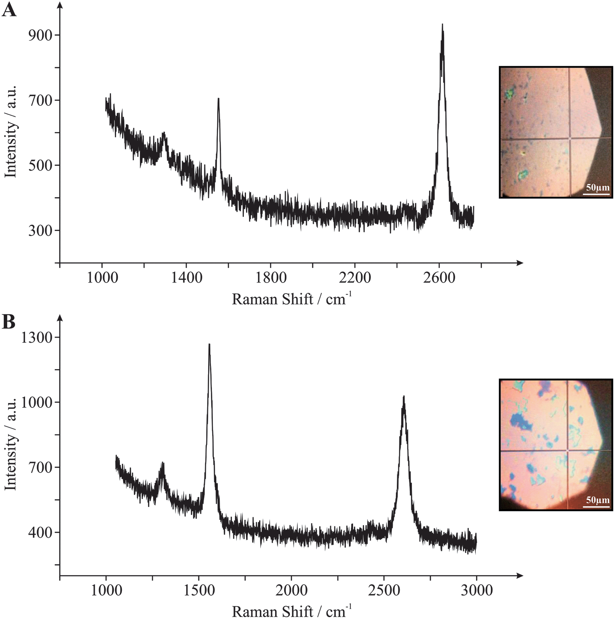 | ||
| Fig. 4 Raman spectroscopy characterisation of monolayer graphene (A) and quasi-graphene (B). Also shown are optical micrographs indicating the probe position utilised. Note that the dark spots indicate few-stacked graphene layers/islands. | ||
Close inspection of the optical micrographs presented in Fig. 4 reveals the presence of thicker graphene islands distributed predominately across the quasi-graphene domain. These multi-layered/defect site domains were probed via Raman spectroscopy and the resultant spectrums are presented in the ESI (Fig. S1†). Surprisingly, analysis of the Raman spectra in these cases at both the mono- and quasi-graphene materials indicate no significant alterations in the reported G/2D band ratios from the values reported above and thus indicate that the number of graphene layers remain unaltered. However, what is evident (again predominately in the case of the quasi-graphene) is an increment in the intensity of the D band (ca. 1330 cm−1) at such sites. This is as expected due to the D band relating directly to the degree of edge plane defects across the graphene surface, where the visible graphitic islands depicted in Fig. 4B give rise to a larger coverage of edge plane like-sites/defects on the quasi-graphene surface, resulting from the exposed ‘edges’ of these few- /multi-layered graphene domains.
Fig. 5 depicts Raman maps that were obtained over a relatively large central area of the graphene surfaces in order to ascertain the overall quality of the graphene present on the monolayer graphene (Fig. 5B and C) and quasi-graphene (Fig. 5E and F) materials. The Raman maps are in excellent agreement with analysis obtained via the individual Raman probe positions and with the AFM images (see Fig. 2 and 3). Fig. 5B and E represent variations in the intensity of the 2D/G peak ratios over the area analysed on the monolayer and quasi-graphene samples respectively, with the darker spots (relative to the scale provided) indicating thicker graphene regions. It is evident that the ‘monolayer graphene’ indeed comprises a single-layer continuous graphene film (indicated by the uniform distribution of ‘lighter pixels’) with occasional defects or islands present (i.e. the darker spots in Fig. 5B). In contrast the quasi-graphene possesses a large number of apparent multi-layered islands distributed across the surface, each with varying thickness as indicated by the severe contrast observed between multiple ‘light’ and ‘dark’ patches. Fig. 5C and F represent variations in the Full Width at Half Maximum (FWHM) of the 2D peak over the areas analysed on the monolayer and quasi-graphene surfaces respectively. The width of the 2D peak is related to the quality of the graphene present, where ‘thinner’ peak widths (darker pixels) indicate pristine single layer graphene and ‘thicker’ (more perturbed) peak widths (lighter pixels) are indicative of thicker graphene layers (as discussed earlier). The even distribution of colour in both maps (Fig. 5C and F) indicates pristine graphene is present on both samples, however relative to the scale provided, the ‘darker’ colouring of the map representing the monolayer graphene (Fig. 5C) is indicative of single-layer graphene relative to the ‘lighter’ colouring of the quasi-graphene indicating the presence of multi-layered graphene.
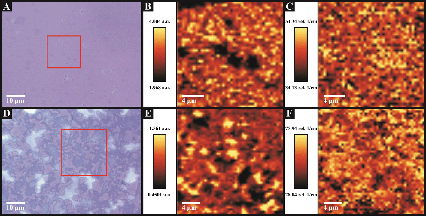 | ||
| Fig. 5 Raman maps and supporting optical micrographs indicating the sample area utilised. Samples were monolayer graphene (A, B and C) and quasi-graphene (D, E and F). Raman maps show: (B and E) 2D/G band ratio, where darker areas represent increased graphene layer numbers; and (C and F) the FWHM of the 2D peak, with lighter areas indicative of thicker graphene domains. | ||
Finally, XPS was conducted on the two graphene materials. De-convolution of the spectra relating to the monolayer graphene domain (Fig. S2, ESI†) reveals it to be composed of 42.73% carbon, 27.72% oxygen and 29.55% silicon. The carbon content comprises of 32.15% corresponding to 284.8 eV which is characteristic of graphitic groups, and 10.27% at 286.6 eV which corresponds to C–O and C![[double bond, length as m-dash]](https://www.rsc.org/images/entities/char_e001.gif) O bonds. Of the oxygen content, 2.1% is comprised from contributions at 287.9 and 533.15 eV, which correspond to CO and C–O groups. Note that contributions from the silicon (29.55%) and remaining oxygen content (25.62%) are a result of the probe depth (ca. 2–3 nm) given that the thin graphene film is supported on top of an oxidised silicon wafer. In considering only the carbon and oxygen contributions arising from the graphene material (which are exposed only to the solution when used in electrochemistry), XPS reveals the monolayer graphene to comprise a O/C ratio of ca. 0.05, which is consistent with that of a low oxygen content of the graphene domain and thus is pristine in nature. De-convolution of the spectra relating to quasi-graphene (Fig. S3, ESI†) reveals it to be composed of 61.50% carbon, 20.06% oxygen and 18.44% silicon (note that due to the probe depth (vide supra) and the increased thickness of the multi-layered graphene surface, in this case the % contribution of carbon has increased and the respective % contribution of silicon has decreased; as expected). The carbon content comprises of 45.62% corresponding to 284.6 eV which is characteristic of graphitic groups, and 8.05 and 6.64% at 285.7 and 286.9 eV respectively which correspond to C–H, CC, C–O and CO bonds. In this case, of the oxygen content 4.4% is comprised from contributions at 287.9 and 533.15 eV. As above, the silicon (18.44%) and the remaining oxygen content (15.66%) contributions are a result of the probe depth utilised (which penetrates the support surface). For the case of the quasi-graphene, considering only the carbon and oxygen contributions arising from the graphene material, XPS reveals a O/C ratio of ca. 0.07, which is consistent with inferences gained through Raman spectroscopy and indicates that the quasi-graphene structure is comprised of pristine graphene domains.
O bonds. Of the oxygen content, 2.1% is comprised from contributions at 287.9 and 533.15 eV, which correspond to CO and C–O groups. Note that contributions from the silicon (29.55%) and remaining oxygen content (25.62%) are a result of the probe depth (ca. 2–3 nm) given that the thin graphene film is supported on top of an oxidised silicon wafer. In considering only the carbon and oxygen contributions arising from the graphene material (which are exposed only to the solution when used in electrochemistry), XPS reveals the monolayer graphene to comprise a O/C ratio of ca. 0.05, which is consistent with that of a low oxygen content of the graphene domain and thus is pristine in nature. De-convolution of the spectra relating to quasi-graphene (Fig. S3, ESI†) reveals it to be composed of 61.50% carbon, 20.06% oxygen and 18.44% silicon (note that due to the probe depth (vide supra) and the increased thickness of the multi-layered graphene surface, in this case the % contribution of carbon has increased and the respective % contribution of silicon has decreased; as expected). The carbon content comprises of 45.62% corresponding to 284.6 eV which is characteristic of graphitic groups, and 8.05 and 6.64% at 285.7 and 286.9 eV respectively which correspond to C–H, CC, C–O and CO bonds. In this case, of the oxygen content 4.4% is comprised from contributions at 287.9 and 533.15 eV. As above, the silicon (18.44%) and the remaining oxygen content (15.66%) contributions are a result of the probe depth utilised (which penetrates the support surface). For the case of the quasi-graphene, considering only the carbon and oxygen contributions arising from the graphene material, XPS reveals a O/C ratio of ca. 0.07, which is consistent with inferences gained through Raman spectroscopy and indicates that the quasi-graphene structure is comprised of pristine graphene domains.
In summary, we have fully characterised our graphene samples which have been fabricated via CVD and transferred onto an inert SiO2 substrate utilising a PMMA transfer process. The monolayer graphene film comprises 97% single-layer graphene domains with occasional small multi-layered graphene islands and possesses a O/C ratio of ca. 0.05, indicating the presence of pristine monolayer graphene. The quasi-graphene film comprises 95% graphene coverage with the thickness of individual graphene domains varying from 1 to 7 layers, with an average of 4 graphene layers (on top of which the multi/few-layered graphene islands are situated) and possesses a O/C ratio of ca. 0.07, indeed indicating the presence of quasi-graphene.
Electrochemistry at monolayer- and quasi-graphene (vs. HOPG)
Prior to the electrochemical utilisation of the fully characterised graphene materials (vide supra) it is first necessary to incorporate the CVD grown graphene chips into a specially designed graphene electrochemical cell connector, giving rise to the respective graphene electrodes. Fig. 6 depicts the experimental set-up of the graphene electrochemical cell utilised to fabricate the graphene electrodes and further details are available in the ‘Experimental section’. The main benefits of this approach is that one is actually electrically wiring to the graphene and thus achieving an efficient electrical connection, but also such that the working electrode area is consistently defined for all the graphene samples being interrogated. Once securely ‘housed’ the design of the electrochemical cell ensures that the graphene material is the only electrochemically active surface that is in contact with the solution during electrochemical measurements. Note that prior work has not fully achieved this, for example, the connection methodology used to connect/wire to the graphene has been exposed to the solution in some cases, which dominates the electrochemical response and gives rise to false indications of electrochemistry at graphene. | ||
| Fig. 6 Schematic diagram of the CVD graphene chip ‘housing’ unit (A). Cross-sectional view of the assembled CVD grown graphene working electrode when fully incorporated (B) for exclusive use with the CVD grown graphene chips/substrates. | ||
Inner-sphere electrochemical characterisation
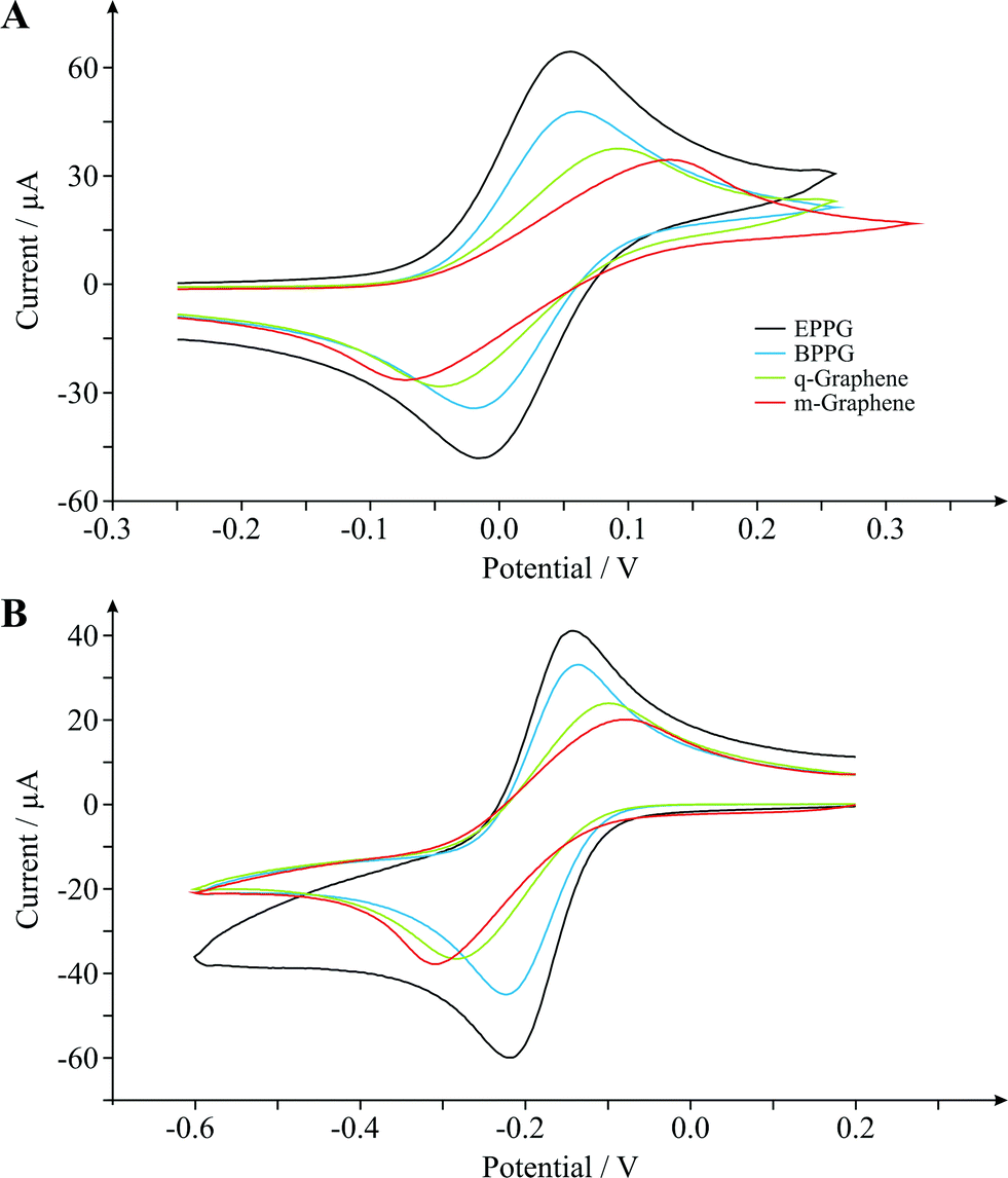
We first turn to electrochemically characterising our CVD grown graphene electrodes towards the widely used inner-sphere electrochemical redox probe, potassium ferrocyanide(II). Fig. 7 depicts typical cyclic voltammograms obtained at well-known and widely characterised EPPG and BPPG electrodes (constructed from HOPG). It is evident that the EPPG and BPPG electrodes both exhibit a pair of well-defined redox peaks, with peak-to-peak separations (ΔEP) of ca. 97.7 and 190.4 mV respectively (at 100 mV s−1); such values are in excellent agreement with prior literature.6 Note that the ΔEP is an important factor to consider in terms of the performance of an electrode material and is used to determine the HET rate (see Experimental section), where smaller ΔEP values represent an increased reversibility in the electrochemistry at the redox probe utilised and thus faster HET kinetics at the given electrode material, which is generally beneficial in numerous instances. The electrochemical response observed at a carbon based electrode material utilising an inner-sphere redox probe is influenced by the density of electronic states (DoS) near the Fermi level of the said material and more significantly by the surface microstructure, for example in terms of the presence of oxygenated species (which are either beneficial or detrimental) or the surface cleanliness.1,17 In particular, it is known that the presence of edge plane like-sites/defects on graphitic materials significantly accelerates the observed electron transfer processes, leading to improved HET at electrodes with a large surface coverage of edge plane like sites.18 Returning to the response observed at the EPPG and BPPG electrodes in Fig. 7, the former exhibits superior electrochemical properties over that of the later since the EPPG electrode has a high global coverage of edge plane sites (which exhibit anomalously fast electron transfer rates over that of basal plane sites).18 Conversely, the BPPG electrode, due to its structure, has a low global coverage of edge plane sites and hence a poor voltammetric activity is exhibited, in terms of a larger ΔEP, when contrasted to the EPPG.1,6 | ||
| Fig. 7 Cyclic voltammetric signatures obtained using potassium ferrocyanide(II) at EPPG (black), BPPG (blue), quasi-graphene (q-graphene, green) and monolayer graphene (m-graphene, red) electrodes. Scan rate shown for each electrode: 100 mV s−1 (vs. SCE). The dotted circle area is a zoomed in portion of the voltammetric window, highlighting the heterogeneous electrode response of the quasi-graphene which gives rise to two distinctive voltammetric signatures. Shown is a separate scan of the region indicated with quasi-graphene using the same parameters except with limiting the potential window. | ||
The electrochemical response of the monolayer graphene (m-Graphene) was next explored towards the Fe(CN)63−/4− probe. A typical cyclic voltammetric profile is depicted in Fig. 7, which exhibits a large ΔEP value of ca. 1147.5 mV (at 100 mV s−1). This response is unique in terms of the extent of the irreversibility of the redox probe observed at the single-layer graphene electrode, with such a large ΔEP value indicating slow HET kinetics. The electrochemical response of the quasi-graphene (q-Graphene) is also presented in Fig. 7 which reveals an interesting occurrence. In addition to a large ΔEP of ca. 1242.7 mV (at 100 mV s−1), again with the large ΔEP indicating slow and unfavourable HET kinetics, closer inspection reveals the presence of an additional voltammetric process, which is shown for clarity as an insert within Fig. 7. This unique latter response indicates changes in the mass transport of the electroactive analyte which is akin to that of a microelectrode, indicating a change from linear (expected for macroelectrodes) to non-linear diffusion (observed at micro/nanoelectrodes). Since the response is only evident when utilising the quasi-graphene electrode it is highly likely that the response originates from the multi-layer islands that are comprised of ca. 4 graphene layers (see characterisation above) which are supported upon a single underlying layer of graphene. Note that the effect of scan rate was explored upon the voltammetric response where a plot of ‘peak height’ against ‘log10 scan rate’ was found to be non-linear over the experimentally chosen scan rate range, which is due to the mass transport being dominated by non-linear diffusion, as has been observed for nano-band type geometric electrodes (deviation from this is observed when linear diffusion becomes dominant; usually following the application of very fast voltammetric scan rates or if the geometric size is micron-sized).17 As shown in the insert of Fig. 7, the response is distinctively and quantitatively different from that observed in the case of the EPPG and BPPG despite comprising the same electrode area. If we assume that such a graphene island is comprised of (on average) 4 graphene layers, where only the edge plane sites are active and neglect any defects upon the basal sheets,18 we have an electrode which is nanoscopic in width and microscopic in length; akin to a nanoband type electrode. As such, the Faradaic current can be predicted by the following equation for the current at a hemi-cylinder of equivalent area:19
| i = 2πnFDCl[1/(In4Θ)] | (1) |
It is important to note that in the case of inner-sphere redox probes the electrochemical response obtained is dependent on both the electronic structure and the content of oxygenated species comprising carbonaceous electrode materials. In the case of quasi-graphene, the structural composition satisfies both these conditions and as such we observe two voltammetric profiles due to the heterogeneous nature of the graphene surface; the response of the graphene islands with adequate carbon–oxygen content and also the response of the underlying supporting graphene (which exhibits a similar voltammetric characteristic to that observed at the pristine monolayer graphene electrode) which has a very low proportion of edge plane defects across its surface and a level of suitable surface oxygen groups residing at these sites, thus overall exhibits large/unfavourable ΔEP values and electrochemical properties.
Outer-sphere electrochemical characterisation
We now consider the electrochemical characterisation of the graphene electrodes using the outer-sphere redox probes TMPD and hexaammine-ruthenium(III) chloride. We utilise these well-known and widely characterised outer-sphere electrochemical redox systems due to the outer-sphere system being dependent only on the electronic structure (DoS) of carbon based electrode materials and thus the degree of edge plane sites, which offers useful insights.Fig. 8A depicts the cyclic voltammetric signatures recorded using the TMPD electrochemical redox probe, where ΔEP values of ca. 63.5, 78.1, 136.7 and 205.1 mV are evident at the EPPG, BPPG, quasi-graphene (q-Graphene) and monolayer graphene (m-Graphene) electrodes respectively (at 100 mV s−1). Similarly, shown in Fig. 8B are the cyclic voltammograms recorded at each of the electrodes of interest towards the Ru(NH3)62+/3+ redox probe where the trend in ΔEP values (HET properties) and the electrochemical responses agree well with those observed for TMPD.
 | ||
| Fig. 8 Cyclic voltammetric signatures obtained using (A) N,N,N′,N′-tetramethyl-para-phenylenediamine (TMPD) and (B) hexaammine-ruthenium(III) chloride at EPPG (black), BPPG (blue), quasi-graphene (q-graphene, green) and monolayer graphene (m-graphene, red) electrodes. Scan rate shown for each electrode: 100 mV s−1 (vs. SCE). | ||
It is clear that in both cases the voltammetric signatures are distinctively different according to a function of the different surface morphologies. For example in the case of Ru(NH3)62+/3+, in the first instance the EPPG and BPPG electrodes give rise to ΔEP values of ca. 68.4 and 83.0 mV respectively (at 100 mV s−1). Such values are in excellent agreement with literature reports where it is well documented that an electrode surface with a large global coverage of edge plane like-sites/defects gives rise to fast heterogeneous electron transfer.6,18 What is insightful, and never before reported in the literature, is that the quasi- and monolayer graphene electrodes give rise to dramatically larger ΔEP separations over that of the graphite electrodes, namely values of ca. 183.1 and 227.1 mV respectively (at 100 mV s−1). Such a response has, to the best of the authors' knowledge, never been reported for graphite/graphene electrodes using this redox probe since the most important factor affecting the rate of reaction is the electronic properties of the electrode, explicitly the potential-dependent electronic DoS near the formal potential of the redox system.20 In terms of graphitic electrodes this is usually observed to a limit where an electrode with a relatively low edge plane coverage (1–10%) gives rise to a near-reversible electrode response.18 In terms of semi- conducting/metallic diamond, the DoS is important and HET becomes worse/slow at diamond with decreasing boron doping levels.20 Thus in this case, in terms of the response of graphene, we observe a clear dependence on the surface morphology with HET which has never before been reported.
Ru(NH3)63+/2+ is classed as an outer-sphere electrochemical redox probe, involving a simple electron transfer on most graphitic electrodes and thus the electrode kinetics are relatively insensitive to the surface microstructure, surface oxides and adsorbed monolayers on sp2 carbon electrodes.1 The rate of reaction is insensitive to surface modification, indicating that electron transfer does not depend on interaction with a surface site or functional group. The most important factor affecting the rate of reaction is the density of electronic states (DoS) near the formal potential of the redox system: as noted above in the case of metallic and graphite electrodes, usually there is not a low DoS and this is seldom an issue, and is only seen at boron-doped diamond electrodes (semi-conducting/semi-metallic diamond) where the ΔEP increases at diamond with decreasing boron-doping level (vide supra).17 In our experiments we observe, for the first time, a clear dependence of the effects of electronic structure (density of states, DoS) upon the electrochemical response of the TMPD and Ru(NH3)63+/2+ probes, as evidenced by the dramatic changes in the ΔEP values, which increase significantly as we utilise fewer graphene layer numbers. Such results indicate that there is a reduction in the HET kinetics at graphene electrodes as the surface composition/morphology comprises fewer layers and thus comprise less edge plane content than those structures consisting of multiple graphene layers viz graphite.
The effective heterogeneous electron transfer rate constant, koeff, was estimated using the Nicholson method (see Experimental section) which is applicable for quasi-reversible systems. Consequently koeff is determined to correspond to 1.81 × 10⁻³, 3.25 × 10⁻³, 19.3 × 10⁻³and 53.2 × 10⁻³ cm s−1 for monolayer-graphene, quasi-graphene, BPPG and EPPG respectively using the TMPD redox probe and to 1.11 × 10⁻³, 1.58 × 10⁻³, 3.80 × 10⁻³ and 8.77 × 10⁻³ cm s−1 for the monolayer-graphene, quasi-graphene, BPPG and EPPG electrodes respectively utilising the Ru(NH3)63+/2+ redox probe. As expected the two data sets support the inferences made earlier where the monolayer graphene electrode possesses the smallest/slowest koeff when contrasted to the quasi-graphene and HOPG alternatives, indicating unfavourable electrochemical properties and a poor electronic structure (DoS) at true single-layer pristine graphene. It is apparent however, that increasing the number of graphene layers from mono- to quasi-graphene (ca. 4 layers) and graphite (≥8, however utilising BPPG in this case) results in an average improvement of ca. 1.7 and 7.5 times faster koeff kinetics generally for when one is utilising the same geometry and only increasing the number of graphene layers (i.e. BPPG possesses same ‘flat’ geometry), and interestingly for EPPG (which has favourable orientation allowing a larger portion of its edge plane sites to be accessible to the solution) this exhibits HET rates on average 21.2 times faster than that of monolayer graphene.1,17
The term “effective electron transfer rate constant” is used since the graphene surfaces are electrochemically heterogeneous and the response is clearly dependent on the population of edge plane like- sites/defects. Using the koeff values determined for the Ru(NH3)63+/2+ redox probe and a value of 0.4 cm s−1 for koedge for Ru(NH3)63+/2+,18 the global coverage of edge plane sites can be readily deduced from koeff(graphene) = koedge(θedge) where the global coverage is given by: θedge(graphene) ≈ Θedge(graphene).18 From analysis of our data (see Fig. 8B) we deduce edge plane coverages (Θedge(graphene)) of 2.2 and 0.95% for the EPPG and BPPG electrodes respectively, which is well within the 1–10% edge plane defect range expected and reported.18 This benchmarks our system giving confidence that the approach will be valid for our graphene surfaces.
Using the same approach we deduce edge plane coverages (Θedge(graphene)) of 0.39 and 0.28% for the quasi- and monolayer-graphene electrodes respectively. This analysis clearly highlights that the % of edge plane coverage is extremely low on our graphene materials, hence explaining the observed voltammetric profiles. Thus the surface of the pristine single-layer graphene comprises a low coverage of edge-plane sites/defects, which given that they are the predominant source of electron transfer,18 results in poor electrochemical performances. However, as the number of graphene layers is increased from monolayer, to quasi- and finally to BPPG, there is an increment in the % coverage of edge plane sites at each of the electrode materials, which is as expected, and resultantly improvements in the electrochemical responses can be observed. Note also that whilst BPPG is that of graphite (HOPG), EPPG has favourable orientation of the edge plane sites and thus exhibits the largest coverage of reactive edge plane sites, and hence the most reversible electrochemistry and superior HET rates are observed at this electrode configuration.
Above we have shown, for the first time, the ‘true’ electronic properties of electrodes comprising single-layer and quasi-layer pristine graphene films. It is evident from the range of electrochemical redox probes utilised (from simple outer-sphere to more complex inner-sphere electron transfer mechanisms) that pristine monolayer graphene exhibits unfavourable HET kinetics in terms of possessing small/low ko values relative to the other graphitic materials utilised with an increased number of graphene layers comprising their structure. Through analysis of the % coverage of edge plane contribution at the various graphitic electrodes, the response of graphene correlates to a low coverage of said sites, which is as expected given its geometry (where its pristine structure comprises predominantly of basal plane contribution).1 Unsurprisingly the graphitic structures utilised with geometries comprising stacked/thicker graphene/graphite structures are shown to possess larger % coverages of electrochemically reactive edge plane sites, where resultantly a correlation between greater edge plane coverage and faster HET rates (improved electrochemical properties) is evident at the graphitic electrodes. In terms of the current literature, never before has monolayer graphene and quasi-graphene been directly compared and contrasted with graphitic electrodes (HOPG). It is satisfying to note that work by Unwin et al.,11 utilising SECM to study the relationship between the structure and properties of micro-graphene domains, supports the observations and inferences drawn in this paper, where it was shown that HET rates at graphene increased as the structure evolved into multi-layered graphene.
It is next insightful to consider the electrochemical response arising from utilising a graphene electrode that possesses a high global coverage of edge plane like-sites/defects. Fig. 9 depicts AFM images of a double-layer CVD grown graphene macrostructure (an optical image of the graphene macrostructure is shown in Fig. S4, ESI†). It is evident that the graphene domains comprising the material possess a large number of surface defect sites, where ‘cracks’ are observable between/throughout the double-layer graphene domains. Also evident is the distinction between the AFM images of the monolayer graphene (Fig. 2) and this two-layer sample (Fig. 9), with the latter possessing a ‘bulky’ topography (i.e. wrinkles and ripples characteristic of single-layer graphene are absent in the double-layer graphene). Raman spectroscopy of the double-layer graphene is shown in Fig. 10A, revealing the two characteristic G and 2D peaks of graphitic materials at ca. 1580 and 2800 cm−1 respectively. As with the previous two graphene materials characterised (see earlier), the high symmetry of the 2D peak indicates the presence of pristine graphene. The intensity ratio of the G and 2D bands (G/2D = 0.86) evident in Fig. 10A indicates the presence of double-layered graphene domains given that the relatively equal intensities (with only a minimal reduction in the G peak relative to the 2D peak) coincide with previous reports for two-layer graphene.12c Raman mapping (which is presented in Fig. 10C and D) was again utilised to validate the overall quality of the graphene sample, which indeed confirmed the inferences gained via AFM and Raman analysis using a single probe position. Fig. 10C and D confirm that the double-layer graphene macrostructure is comprised of a uniform two-layer graphene domain, on top of which occasional graphitic islands exist. Also evident in Fig. 10C is an observable ‘crack’, which indicates the presence of an edge plane like-site/defect (i.e. a grain boundary). XPS was next conducted on the double-layer graphene material. De-convolution of the spectra (Fig. S5, ESI†) reveals a composition of 29.21% carbon, 30.12% oxygen and 39.06% silicon. The carbon content comprises of 18.7% corresponding to 284.5 eV which is characteristic of graphitic groups, and 8.73 and 1.78% at 286.1 and 288.9 eV respectively which correspond to C–H, CC, C–O and CO bonds. Of the oxygen content, 0.82% is comprised from contributions at 535.4 eV. The silicon (39.1%) and the remaining oxygen content (29.3%) contributions are a result of the probe depth utilised (which penetrates the support surface, see earlier). For the case of the double-layer defect-graphene, considering only the carbon and oxygen contributions arising from the graphene material, XPS reveals a O/C ratio of ca. 0.03. In summary, the physicochemical characterisation of the double-layer graphene film shows it to be comprised of 95% graphene coverage, with an average thickness of two-layers across the graphene domains, however with a large number of structural defects/islands giving rise to a high global coverage of edge plane like-sites/defects.
 | ||
| Fig. 9 AFM images of the double-layer defect-graphene, successive images are progressively focused into the sample. | ||
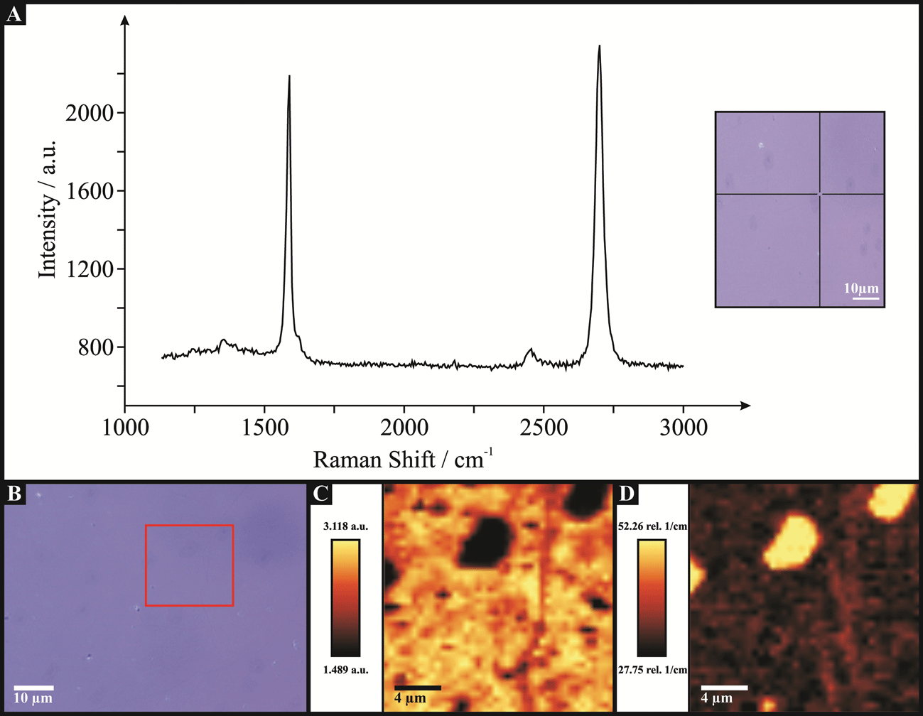 | ||
| Fig. 10 Characterisation of the double-layer defect-graphene macrostructure. (A) Raman spectroscopy, with an optical micrograph (inset) indicating the single probe position utilised. Raman maps and a supporting optical micrograph indicating the sample area utilised are reported in B, C and D. (C) 2D/G band ratio, where darker areas represent increased graphene layer numbers. (D) FWHM of the 2D peak, with lighter areas indicative of thicker graphene domains. | ||
The electrochemical response of the (edge plane abundant) double-layer defect-graphene electrode is shown in Fig. 11 towards the outer-sphere redox probes TMPD and Ru(NH3)63+/2+, with ΔEP values of ca. 112.3 and 128.5 mV respectively (at 100 mV s−1). Through employment of the appropriate scan rate studies the koeff was estimated as reported earlier, corresponding to 6.53 × 10⁻³ and 3.12 × 10⁻³ cm s−1 at the TMPD and Ru(NH3)63+/2+ redox probes respectively; with the latter value relating to an edge plane coverage (Θedge(graphene)) of 0.78% for the double-layer defect-graphene electrode. Through comparison of the respective koeff values, it is clear that the double-layer defect-graphene exhibits favourable HET rates relative to the pristine monolayer and quasi-graphene electrodes. Also evident is that the performance of the double-layer graphene does not surpass that observed at the HOPG electrodes. Considering that the domain edges are somewhat sealed in monolayer graphene, while the edge of basal planes are exposed in HOPG, it is the response at double-layer defect-graphene that is interesting and of critical importance here, because it is neither bulk nor monolayer. Given that favourable ko values are observed at the double-layer defect-graphene relative to the monolayer graphene (with few double-layered islands distributed across its surface, see characterisation), it is apparent that simply introducing an increased number of edge plane defect sites across the surface of a graphene macrostructure (opposed to increasing the number of graphene layers in order to give rise to increased edge plane coverage) results in improvements in the electrochemical behaviour of said electrode material. Hence, in support of earlier inferences, there is a clear correlation relating observed improvements in the electrochemical performance of the given graphitic electrode to increased global coverages of edge plane like-sites/defects comprising the electrode surface.
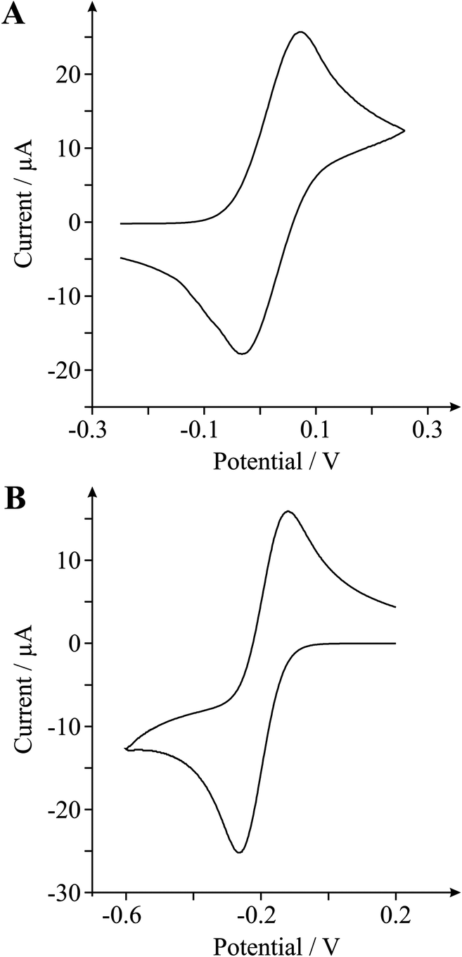 | ||
| Fig. 11 Cyclic voltammetric signatures obtained using the double-layer defect-graphene electrode at (A) N,N,N′,N′-tetramethyl-para-phenylenediamine (TMPD) and (B) hexaammine-ruthenium(III) chloride. Scan rate: 100 mV s−1 (vs. SCE). | ||
A further experiment was conducted where the intra-repeatability of each graphene electrode was tested. Following the initial experiments performed over the voltammetric scan rates stated, the graphene electrodes were taken out of the test solution (and removed from the CVD ‘housing’ unit) before being thoroughly rinsed/washed with deionised water and the voltammetry repeated (once efficiently ‘re-housed’) using the Ru(NH3)63+/2+ redox probe (N = 3). Interestingly, over the course of the repeat experiments the electrochemical response was observed to degrade (resulting in larger ΔEP and smaller IP values for the later repeats) at each of the graphene electrodes utilised. The % Relative Standard Deviation (% RSD), when calculated as an average across the full range of voltammetric scan rates utilised, was found to be 60.8% (ΔEP) and 20.5% (IP) using the monolayer graphene, 43.3% (ΔEP) and 13.7% (IP) using the double-layer defect-graphene, and 14.0% (ΔEP) and 8.3% (IP) using the quasi-graphene electrode. This observation has never been reported before in the literature when utilising graphene electrodes and is likely due to the physical stresses applied on the sample surface when washing said electrodes (disrupting/destroying the graphene surface) or through voltammetric induced surface changes (although repeat voltammetric scans eluding the ‘washing’ step revealed no such changes). The exact origin is unknown at this time and could possibly indicate a limitation of these graphene electrodes; further work is underway. Of further interest is that the % RSD values appear to reduce with increased numbers of graphene layers, where it is likely that the underlying graphene layers may become exposed on multi-layered structures and contribute such that the electrochemical response is ‘maintained’. Conversely, such underlying layers are not ‘available’ with respect to the single-layer graphene sample, resulting in the degradation of the electrochemical response relative to the monolayer surface.
Last, it is illuminating to consider the further potential implications of graphene's geometry and thus unfavourable HET properties on its electroanalytical performance (the peak height, IP). Re-inspection of Fig. 7 and 8 reveal that in terms of the voltammetric IP, monolayer graphene exhibits reduced magnitudes in the current passed at each of the redox probes utilised when its performance is contrasted to that of the other graphitic materials. Again (as observed above in the case of considering the HET rates) there is a distinct correlation evident between the % coverage of edge plane sites and the magnitude of the electroanalytical signal (IP) produced. This work has shown that increasing the number of graphene layers comprising an electrode material (evolution from monolayer to quasi-graphene and to BPPG) results in improved electrochemical responses, with further improvements evident when altering the geometry to exhibit higher degrees of edge plane sites (such as the distinct BPPG and EPPG responses). As the monolayer graphene has the lowest proportion of edge plane like/sites-defects it will give rise to the smallest peak current since the peak current is proportional to the ‘active area’ and the analytical response will be far from optimal, with the best and most favourable responses originating from multi-layer graphene (which is structurally similar to graphite); hence an edge plane pyrolytic graphite electrode is the obvious choice for electroanalysis since it can additionally be mechanically polished between voltammetric experiments.21
Conclusions
In summary, we have, for the first time, directly shown a correlation in the structure of graphene, in terms of its number of layers directly upon its electrochemical performance. It is found that the macroscopic electrochemical response of graphene is highly dependent on the number of graphene layers which determines its electrochemical behaviour, which in turn corresponds to the density of edge plane like-site/defects comprising its structure.Given that pristine monolayer graphene has a low degree of edge plane coverage compared to the multi-layered structures of quasi-graphene and HOPG, in comparison it possesses poor/slow electrochemical properties in terms of HET kinetics. In scenarios when favourable/fast HET rates are required, recourse to quasi-graphene and edge plane of HOPG is suggested. Note that manipulation of the graphene structure, in terms of orientation (such as exposing more edge) or through the introduction of surface edge plane like-sites/defects, will result in beneficial alterations in the observed electrochemical properties;22 which was shown herein utilising a defect abundant double-layer graphene electrode. The ability to tailor graphene's electrochemical response through surface composition/control makes this a fascinating area of study.
This work is an important and fundamental contribution to those studying the electron transfer properties of graphene since it provides the first comparison of true mono- vs. quasi-graphene, highlighting that the electrochemical response (electron transfer) is dependent on the graphene’s electronic structure.
Experimental section
All chemicals used were of analytical grade and were used as received from Sigma-Aldrich without any further purification. All solutions were prepared with deionised water of resistivity not less than 18.2 MΩ cm and were vigorously degassed prior to electrochemical measurements with high purity, oxygen free nitrogen. Test solutions (potassium ferrocyanide(II), hexaammine-ruthenium(III) chloride and N,N,N′,N′-tetramethyl-para-phenylenediamine (TMPD)) were utilised at a concentration of 1 mM separately in solution, with each containing 0.1 M potassium chloride as the supporting electrolyte.Voltammetric measurements were carried out using an ‘Autolab PGSTAT 101’ (Metrohm Autolab, The Netherlands) potentiostat. All measurements were conducted using a three electrode system. Working electrodes were either: a commercially obtained CVD synthesised monolayer graphene film supported on an oxidised silicon wafer; a commercially obtained CVD synthesised few-layer graphene (termed quasi-graphene) film supported on an oxidised silicon wafer; a commercially obtained CVD synthesised double-layer graphene film (with a high level of surface/structural defects) supported on an oxidised silicon wafer; EPPG (Le Carbone, Ltd. Sussex, U.K) which was machined into a 4.9 mm diameter with the disc face parallel to the edge plane as required from a slab of HOPG (highest grade available: SPI-1, equivalent to Union Carbide's ZYA grade, with a lateral grain size, La of 1–10 μm and 0.4 ± 0.1° mosaic spread); or alternatively BPPG which was machined as per the EPPG however with the disc face parallel with the basal plane as required. A platinum wire counter/auxiliary electrode and a saturated calomel electrode (SCE) reference (Radiometer, Copenhagen, Denmark) completed the circuit. Note that where voltammetric scan rate studies are employed, the following increments were utilised: 5, 15, 25, 50, 75, 100, 150, 200, 250, 300, 400 and 500 mV s−1.
For employment of the CVD chip working electrodes an electrochemical cell was utilised as described previously by our group.23 Essentially, the CVD chip was secured into a polytetrafluoroethylene (PTFE) housing unit with a silicone O-ring defining the working surface (diameter, 4.9 mm) and a steel contact making connection to the back of the chip, which via the use of silver conductive paint (applied to cover the back and sides of the chip in their entirety) ensures electrical conductivity from the front ‘working surface’ of the electrode to the electrode connector (to which a lead for the working electrode can be attached). Fig. 6 details the experimental set-up, adapted specifically for electrochemical measurements utilising CVD grown graphene. This unique cell design ensures that graphene is the only electrochemically active surface that is in contact with the solution during electrochemical measurements and allows the direct electrical wiring of the graphene – but without worry that the connecting silver conductive paint might be exposed to the solution giving rise to false voltammetry. Using this electrochemical cell, the exposed working electrode area is consistently 0.189 cm2 for all graphene samples studied, which is consistent with the HOPG electrodes utilised.
The commercially available CVD synthesised monolayer graphene film was obtained from ‘Graphene Supermarket’ (Reading, MA, USA)24 and is known as ‘Monolayer Graphene on 285 nm SiO2 Wafer’. The single layer continuous graphene film (ca. 97% graphene coverage (95% monolayer) with occasional holes, cracks and small multi-layer islands) comprises graphene grains of different crystallographic orientations (polycrystalline in nature) and is grown utilising a copper foil (25 μm thick) catalyst via a CVD synthesis method (ca. 1000 °C (cooling rate 40–300 °C min−1) with H2/CH4 precursor (0.06 sccm and partial pressure 0.5 Torr) for less than 3 minutes growth time).9,25 Following growth the graphene film is transferred onto an oxidised silicon wafer (electrochemically inert supporting substrate) via a poly-methyl methacrylate (PMMA) assisted transfer method, as previously reported and characterised;9,14a,25a,26 note, the exact details are proprietary information.24
The commercially available CVD synthesised quasi-graphene film was obtained from ‘Graphene Supermarket’ (Reading, MA, USA)24 and is known as ‘Multilayer Graphene on 285 nm SiO2Wafer’. The multi-layer (or few-layer) continuous graphene film (ca. 95% graphene coverage with occasional holes and cracks) comprises graphene grains of polycrystalline nature. The multi-layer graphene film is not uniform, which is evident through observation of the optical microscopy image depicted in Fig. 1B where a ‘patchwork’ like appearance indicates ‘patches’ of different thicknesses; the thickness varies from 1 to 7 layers, with an average of 4 graphene layers (the graphene layers within the same ‘patch’ are aligned relative to each other (there is a graphitic AB-stacking order)).24 The multi/few-layered continuous graphene film is grown utilising a nickel foil (500 nm thick) catalyst via a CVD synthesis method (ca. 1000 °C (cooling rate 100 °C min−1) with CH4 precursor (10 sccm (H2, 1400 sccm), ambient pressure) for ca. 5 minutes growth time),9,25b,27 after which the graphene film is transferred onto an oxidised silicon wafer via a PMMA assisted transfer method;9,25a,26,27 the exact details are proprietary information.24
The commercially available CVD synthesised double-layer graphene film was obtained from ‘Graphene Supermarket’ (Reading, MA, USA)24 and is known as ‘Single/Double Layer Graphene on 285 nm SiO2 Wafer’. The mono-/bi-layer continuous graphene film (ca. 95% graphene coverage (up to ca. 30% coverage is double-layer graphene islands) with occasional holes and cracks) comprising graphene grains of different crystallographic orientations (polycrystalline in nature) is grown utilising a modified method of the aforementioned CVD process. For example, a copper foil (206 nm thick) catalyst is utilised via a CVD synthesis method (ca. 800 °C (cooling rate 40–300 °C min−1) with H2/CH4 precursor (5 sccm and partial pressure 0.39 Torr) for ca. 10 minutes growth time),9,25 after which the graphene film is transferred onto an oxidised silicon wafer via the PMMA assisted transfer method, as previously reported and characterised.9,14a,25a,26 The exact details are proprietary information.24
Note that other than securely ‘housing’ the CVD grown graphene chips/electrodes into the appropriate ‘housing’ unit prior to electrochemical measurements, the graphene films were used as received from the supplier without any further modification. The graphene ‘wafer’ macrostructures, before being adapted into electrodes using the electrode ‘housing cell/unit’, are 1× 1 cm2 in size. The manufacturer reports a resistivity of ca. 660–1500 and 500–1500 Ω per □ across the lateral surface of the monolayer- and quasi-graphene wafers respectively.24 Attempts were made to independently measure the resistivity; however, due to the fragile nature of the graphene surfaces we were unable to ascertain a reliable/reproducible response.
Atomic Force Microscopy (AFM) data was collected in TappingMode™ using a Veeco Dimension 3100 scanning probe microscope with a NanoScope V controller; images were produced using NanoScope analysis v1.4. Raman spectra were recorded using LabRam (Jobin-Ivon) with a confocal microscope (× 100 objective) spectrometer with a He–Ne laser at 633 nm excitation at a very low laser power level (0.9 mW) to avoid any heating effect (beam width ca. 100 μm). X-ray photoelectron spectroscopy (XPS, K-Alpha, Thermo Scientific) was used to analyse the chip surface. All spectra were collected using Al–K radiation (1486.6 eV), monochromatised by a twin crystal monochromator, yielding a focused X-ray spot with a diameter of 400 μm, at 3 mA × 12 kV. The alpha hemispherical analyser was operated in the constant energy mode with survey scan pass energies of 200 eV to measure the whole energy band and 50 eV in a narrow scan to selectively measure the particular elements. Thus, XPS was used to provide the chemical bonding state as well as the elemental composition of the surface. Charge compensation was achieved with the system flood gun that provides low energy electrons and low energy argon ions from a single source.
The values of koeff were determined utilising a method developed by Nicholson,28 using the following equation, ψ = ko[πDnυF/(RT)]−1/2 where ψ is a kinetic parameter, D is the diffusion coefficient, n is the number of electrons involved in the process, F is the Faraday constant, R the gas constant and T the temperature. The kinetic parameter, ψ, is tabulated as a function of ΔEP at a set temperature (298 K) for a one-step, one electron process (where the transfer coefficient, α = 0.5).1,17,28 The function of ψ (ΔEP), which fits Nicholson's data, for practical usage (rather than producing a working curve) is given by:17,29ψ = (−0.6288 + 0.021X)/(1 − 0.017X) where X = ΔEP is used to determine ψ as a function of ΔEP from the experimentally recorded voltammetry. From this, a plot of ψ against [πDnυF/(RT)]−1/2 allows the koeff to be readily determined. The diffusion coefficients used for calculations were as follows: Fe(CN)63−/4−, D = 6.5 × 10⁻⁶ cm2 s−1;30,31 Ru(NH3)62+/3+, D = 9.1 × 10⁻⁶ cm2 s−1;30,31 TMPD, D = 6.6 × 10⁻⁶ cm2 s−1.32 Note, all D values are reported in the presence of 0.1 M KCl supporting electrolyte and koeff values are deduced over the entire scan rate range of 5–500 mVs−1 unless stated otherwise. A commercial simulation package (Digisim™) was utilised where appropriate to support the Nicholson analysis and additionally when this was not suitable to determine koeff values.
References
- D. A. C. Brownson, D. K. Kampouris and C. E. Banks, Graphene electrochemistry: fundamental concepts through to prominent applications, Chem. Soc. Rev., 2012, 41, 6944–6976 RSC.
- K. S. Novoselov, D. Jiang, F. Schedin, T. J. Booth, V. V. Khotkevich, S. V. Morozov and A. K. Geim, Two-dimensional atomic crystals, Proc. Natl. Acad. Sci. U. S. A., 2005, 102, 10451–10453 CrossRef CAS PubMed.
- (a) A. K. Geim and K. S. Novoselov, The rise of graphene, Nat. Mater., 2007, 6, 183–191 CrossRef CAS PubMed; (b) Y. Zhu, S. Murali, W. Cai, X. Li, J. W. Suk, J. R. Potts and R. S. Ruoff, Graphene and graphene oxide: synthesis, properties, and applications, Adv. Mater., 2010, 22, 3906–3924 CrossRef CAS PubMed.
- (a) D. A. C. Brownson, D. K. Kampouris and C. E. Banks, An overview of graphene in energy production and storage applications, J. Power Sources, 2011, 196, 4873–4885 CrossRef CAS PubMed; (b) T. Gan and S. Hu, Electrochemical sensors based on graphene materials, Microchim. Acta, 2011, 175, 1–19 CrossRef CAS; (c) X. Huang, Z. Zeng, Z. Fan, J. Liu and H. Zhang, Graphene-based electrodes, Adv. Mater., 2012, 24, 5979–6004 CrossRef CAS PubMed.
- D. A. C. Brownson, L. C. S. Figueiredo-Filho, X. Ji, M. Gómez-Mingot, J. Iniesta, O. Fatibello-Filho, D. K. Kampouris and C. E. Banks, Freestanding three-dimensional graphene foam gives rise to beneficial electrochemical signatures within non-aqueous media, J. Mater. Chem. A, 2013, 1, 5962–5972 CAS.
- D. A. C. Brownson, L. J. Munro, D. K. Kampouris and C. E. Banks, Electrochemistry of graphene: not such a beneficial electrode material?, RSC Adv., 2011, 1, 978–988 RSC.
- W. Li, C. Tan, M. A. Lowe, H. D. Abruna and D. C. Ralph, Electrochemistry of individual monolayer graphene sheets, ACS Nano, 2011, 5, 2264–2270 CrossRef CAS PubMed.
- A. T. Valota, I. A. Kinloch, K. S. Novoselov, C. Casiraghi, A. Eckmann, E. W. Hill and R. A. W. Dryfe, Electrochemical behavior of monolayer and bilayer graphene, ACS Nano, 2011, 5, 8809–8815 CrossRef CAS PubMed.
- D. A. C. Brownson and C. E. Banks, The electrochemistry of CVD graphene: progress and prospects, Phys. Chem. Chem. Phys., 2012, 14, 8264–8281 RSC.
- A. M. Bond, D. Luscombe, K. B. Oldham and C. G. Zoski, A comparison of the chronoamperometric response at inlaid and recessed disc microelectrodes, J. Electroanal. Chem. Interfacial Electrochem., 1988, 249, 1–14 CrossRef CAS.
- A. G. Guell, N. Ebejer, M. E. Snowden, J. V. Macpherson and P. R. Unwin, Structural correlations in heterogeneous electron transfer at monolayer and multilayer graphene electrodes, J. Am. Chem. Soc., 2012, 134, 7258–7261 CrossRef CAS PubMed.
- (a) D. Graf, F. Molitor, K. Ensslin, C. Stampfer, A. Jungen, C. Hierold and L. Wirt, Spatially resolved Raman spectroscopy of single- and few-layer graphene, Nano Lett., 2007, 7, 238–242 CrossRef CAS PubMed; (b) A. C. Ferrari, Raman spectroscopy of graphene and graphite: disorder, electron–phonon coupling, doping and nonadiabatic effects, Solid State Commun., 2007, 143, 47–57 CrossRef CAS PubMed; (c) Y. Y. Wang, Z. H. Ni, T. Yu, Z. X. Shen, H. M. Wang, Y. H. Wu, W. Chen and A. T. S. Wee, Raman studies of monolayer graphene: the substrate effect, J. Phys. Chem. C, 2008, 112, 10637–10640 CrossRef CAS.
- C. Mattevi, H. Kim and M. Chhowalla, A review of chemical vapour deposition of graphene on copper, J. Mater. Chem., 2011, 21, 3324–3334 RSC.
- (a) X. Li, Y. Zhu, W. Cai, M. Borysiak, B. Han, D. Chen, R. D. Piner, L. Colombo and R. S. Ruoff, Transfer of large-area graphene films for high-performance transparent conductive electrodes, Nano Lett., 2009, 9, 4359–4363 CrossRef CAS PubMed; (b) J. Kang, D. Shin, S. Bae and B. H. Hong, Graphene transfer: key for applications, Nanoscale, 2012, 4, 5527–5537 RSC.
- A. Ambrosi and M. Pumera, Electrochemistry at CVD grown multilayer graphene transferred onto flexible substrates, J. Phys. Chem. C, 2013, 117, 2053–2058 CAS.
- D. A. C. Brownson and C. E. Banks, CVD graphene electrochemistry: the role of graphitic islands, Phys. Chem. Chem. Phys., 2011, 13, 15825–15828 RSC.
- D. A. C. Brownson and C. E. Banks, The handbook of graphene electrochemistry, Springer Publishing, London, U.K., 2014 Search PubMed.
- (a) T. J. Davies, M. E. Hyde and R. G. Compton, Nanotrench arrays reveal insight into graphite electrochemistry, Angew. Chem., Int. Ed., 2005, 44, 5121–5126 CrossRef CAS PubMed; (b) T. J. Davies, R. R. Moore, C. E. Banks and R. G. Compton, The cyclic voltammetric response of electrochemically heterogeneous surfaces, J. Electroanal. Chem., 2004, 574, 123–152 CrossRef CAS PubMed.
- K. R. Wehmeyer, M. R. Deakin and R. M. Wightman, Electroanalytical properties of band electrodes of submicrometer width, Anal. Chem., 1985, 57, 1913–1916 CrossRef CAS.
- M. C. Granger, M. Witek, J. Xu, J. Wang, M. Hupert, A. Hanks, M. D. Koppang, J. E. Butler, G. Lucazeau, M. Mermoux, J. W. Strojek and G. M. Swain, Standard electrochemical behavior of high-quality, boron-doped polycrystalline diamond thin-film electrodes, Anal. Chem., 2000, 72, 3793–3804 CrossRef CAS.
- C. E. Banks and R. G. Compton, New electrodes for old: from carbon nanotubes to edge plane pyrolytic graphite, Analyst, 2006, 131, 15–21 RSC.
- C. X. Lim, H. Y. Hoh, P. K. Ang and K. P. Loh, Direct voltammetric detection of DNA and pH sensing on epitaxial graphene: an insight into the role of oxygenated defects, Anal. Chem., 2010, 82, 7387–7393 CrossRef CAS PubMed.
- D. A. C. Brownson, R. V. Gorbachev, S. J. Haigh and C. E. Banks, CVD graphene vs. highly ordered pyrolytic graphite for use in electroanalytical sensing, Analyst, 2012, 137, 833–839 RSC.
- Graphene-Supermarket: http://www.graphene-supermarket.com (accessed 28th May 2013).
- (a) X. Li, W. Cai, J. An, S. Kim, J. Nah, D. Yang, R. Piner, A. Velamakanni, I. Jung, E. Tutuc, S. K. Banerjee, L. Colombo and R. S. Ruoff, Large-area synthesis of high-quality and uniform graphene films on copper foils, Science, 2009, 324, 1312–1314 CrossRef CAS PubMed; (b) X. Li, W. Cai, L. Colombo and R. S. Ruoff, Evolution of graphene growth on Ni and Cu by carbon isotope labelling, Nano Lett., 2009, 9, 4268–4272 CrossRef CAS PubMed.
- (a) X. Liang, B. A. Sperling, I. Calizo, G. Cheng, C. A. Hacker, Q. Zhang, Y. Obeng, K. Yan, H. Peng, Q. Li, X. Zhu, H. Yuan, A. R. H. Walker, Z. Liu, L.-M. Peng and C. A. Richter, Toward clean and crackless transfer of graphene, ACS Nano, 2011, 5, 9144–9153 CrossRef PubMed; (b) M. Her, R. Beams and L. Novotny, Graphene transfer with reduced residue, Phys. Lett. A, 2013, 377, 1455–1458 CrossRef CAS PubMed.
- A. Reina, S. Thiele, X. Jia, S. Bhaviripudi, M. S. Dresselhaus, J. A. Schaefer and J. Kong, Growth of large-area single- and bi-layer graphene by controlled carbon precipitation on polycrystalline Ni surfaces, Nano Res., 2009, 2, 509–516 CrossRef CAS.
- R. S. Nicholson, Theory and application of cyclic voltammetry for measurement of electrode reaction kinetics, Anal. Chem., 1965, 37, 1351–1355 CrossRef CAS.
- I. Lavagnini, R. Antiochia and F. Magno, An extended method for the practical evaluation of the standard rate constant from cyclic voltammetric data, Electroanalysis, 2004, 16, 505–506 CrossRef CAS.
- R. N. Adams, Electrochemistry at solid electrodes, Marcel Dekker, Inc., New York, U.S.A., 1969 Search PubMed.
- C. E. Banks, R. G. Compton, A. C. Fisher and I. E. Henley, The transport limited currents at insonated electrodes, Phys. Chem. Chem. Phys., 2004, 6, 3147–3152 RSC.
- M. J. Moorcroft, N. S. Lawrence, B. A. Coles, R. G. Compton and L. N. Trevani, High temperature electrochemical studies using a channel flow cell heated by radio frequency radiation, J. Electroanal. Chem., 2001, 506, 28–33 CrossRef CAS.
Footnote |
| † Electronic supplementary information (ESI) available. See DOI: 10.1039/c3nr05643k |
| This journal is © The Royal Society of Chemistry 2014 |