Transparent free-standing metamaterials and their applications in surface-enhanced Raman scattering
Xinglin
Wen
a,
Guangyuan
Li
a,
Jun
Zhang
a,
Qing
Zhang
a,
Bo
Peng
a,
Lai Mun
Wong
c,
Shijie
Wang
*c and
Qihua
Xiong
*ab
aDivision of Physics and Applied Physics, School of Physical and Mathematical Sciences, Nanyang Technological University, Singapore 637371. E-mail: Qihua@ntu.edu.sg
bNOVITAS, Nanoelectronics Centre of Excellence, School of Electrical and Electronic Engineering, Nanyang Technological University, Singapore 639798
cInstitute of Materials Research & Engineering, Agency for Science, Technologies and Research, 3 Research Link, Singapore 117602. E-mail: sj-wang@imre.a-star.edu.sg
First published on 7th October 2013
Abstract
Integration of metamaterials onto a flexible substrate can provide many advantages such as transparency, deformability, light weight and biocompatibility. Here we demonstrate a simple and convenient nickel sacrificial layer-assisted transfer method to fabricate visible–near infrared (IR) metamaterials embedded into a thin polydimethylsiloxane (PDMS) film. Both the structures and the optical properties are maintained after transferring into the PDMS film from a rigid substrate. This PDMS-based metamaterial can behave as a high performance surface enhanced Raman scattering (SERS) device with tunable plasmonic bands, which decouple the preparation of SERS structure and the linkage of targeted molecules to the plasmonic structures. By simply covering the PDMS metamaterials device on the surface with molecules of interest, we demonstrate the application of 2-naphthalenethiol molecules self-assembled on a Au film, highlighting the considerable potential of these PDMS metamaterials as a SERS stamp onto any other substrate. What's more, the PDMS-based nanostructures offer a representative model to investigate the interaction between the plasmonic nanostructure and the substrate consisting of different materials by placing PDMS on the surface of the substrate.
Introduction
Integration of electronic and photonic components onto flexible substrates has attracted considerable attention recently. Many unique systems have been introduced based on flexible substrates, for instance, stretchable nanopillar-array solar cells,1 high-performance paper-like displays,2 highly ordered silicon nanowires on plastic for chemical and biological sensing,3 and nanowire array FETs (field effect transistors) on polyimide functioning as an artificial electronic skin.4 Compared with the conventional rigid substrates like silicon or glass, flexible substrates such as plastic or polymers have advantages of transparency, deformability, non-planarity, light weight and biocompatibility.Within the past few years, metamaterials have been emerging as a new approach to control the properties of materials as desired.5–9 Analogous to the naturally occurring bulk materials which are composed of atoms or molecules, metamaterials are constructed by properly arranging “artificial atoms”. Metamaterials primarily gain their unprecedented properties from the specific structures rather than the chemical composition, ranging from negative refractive index, to applications as an invisibility cloak and superlenses.7,10–12 Attaching metamaterials to a flexible substrate provides additional benefits in practical applications. For instance, 3D metamaterials have been attempted by stacking the metamaterials fabricated on a plastic or polyimide substrate layer by layer.13 Within the flexible matrix, tunable and active metamaterials can be achieved by applying a strain to the matrix to alter the shape and the coupling distance of the metamaterials’ components.14–16 Moreover, a flexible substrate can lower the permittivity and reduce the dielectric loss of supporting media,17 which are important factors affecting the sensitivity of sensing applications.18 The deformability of the substrate provides a convenient way to integrate metamaterials on a non-planar surface,15,17 for instance, wrapping the devices around a curved object to serve as an invisibility cloak. However, the fabrication of flexible metamaterials is not trivial, especially for the metamaterials operating in the visible–near IR range whose size is on the order of tens of nanometers. Two methods have been reported to realize flexible metamaterials: direct patterning and the transfer method. Direct patterning of terahertz metamaterials on polyimide substrates with photolithography has been demonstrated. The success is largely attributed to the large micrometer-sized resonator structures.19 Furthermore, we have recently realized visible–near IR split-ring resonator (SRR) metamaterials directly fabricated on plastic poly(ethylene naphthalate) (PEN) substrates by electron beam lithography (EBL).20 Nevertheless, there are considerable limitations in the fabrication of visible–near IR metamaterials on a more flexible matrix such as PDMS polymer with either direct photolithography or EBL methods, mainly because of the deformability and insulating properties of PDMS. For the transfer method, usually the patterns are generated on a rigid substrate such as silicon first, followed by transfer of the replica to the polymer by etching the substrate as Pryce and Aydin et al. demonstrated.16 Etching of silicon wafer is not cost-effective and it requires accurate control of the etch rate and time to avoid over-etching. In addition, a surface chemistry treatment is necessary to strengthen the bonding between the polymer and the metamaterial’s surface. Herein, we report a simple, effective and convenient Ni sacrificial layer assisted transfer method to fabricate visible–near IR metamaterials on a thin PDMS film. Our method relies on the property that Ni will separate from a SiO2 layer readily in the presence of water. A subsequent HCl solution etching simply removes the Ni layer, leaving the metamaterials embedded in PDMS.
Surface enhanced Raman scattering (SERS) is a remarkable technique which can enhance the Raman signal dramatically when analytes are in close proximity to metal nanoparticles.21–25 The signal enhancement emerges from the strong electromagnetic field around the nanoparticle surface due to the surface plasmon resonance.22,26,27 In previous years, many substrates have proven to be SERS-active, such as rough metal electrodes,28,29 metal colloidal films,30 nanoparticles on a rigid substrate,31–33 and many sandwiched SERS-active substrates.34–37 However, for conventional SERS-active substrates, where the substance or molecules to be probed are absorbed on the nanoparticles’ surface, one has to consider the substrate effects and the surface chemistry between the nanoparticles and the analytes. Many new SERS strategies that can separate the analytes from the SERS-active substrates have been introduced, such as tip-enhanced Raman spectroscopy (TERS)38,39 and shell-isolated nanoparticle-enhanced Raman spectroscopy (SHINERS).40 For TERS, there is only one tip that serves as a signal amplifier and the enhancement is thus limited. On the other hand, SHINERS is also limited because it is not convenient to apply these isolated nanoparticles in solution phase onto any surface at will. Lu et al. have also reported a convenient SERS method based on nanoparticles embedded in PDMS;35,41 the only drawback is that in this method it is difficult to control the density and size of these nanoparticles accurately. One of the biggest challenges in SERS is to fabricate a highly regular, well-defined and reproducible SERS-active substrate. It is well understood that the Raman enhancement depends on the size and shape of the metal nanostructures; any deviation in the size, shape and orientation of the metal nanostructures will affect the detection sensitivity.42 It is thus desirable to achieve well-defined, highly controlled and reproducible SERS-active substrates. Herein, utilizing metamaterials embedded in PDMS as a SERS platform, Raman enhancement can be achieved by covering the PDMS–metamaterials with analytes residing on the surface. This SERS strategy not only makes it possible to separate the analytes from the substrate, but also takes advantage of the well-defined, highly controlled, tunable and reproducible metamaterials patterns when we use EBL to define these metamaterials’ structures.
Results and discussions
Split-ring resonators (SRRs) are widely used metamaterial components, which have both an electric and magnetic response.43 The electric resonance arises from the dipole resonance under the excitation of light, while the origin of the magnetic resonance emerges from the coupling of the electric and magnetic fields.44 It is the magnetic resonance that makes these structures distinguished and termed “metamaterials”. SRRs can be simplified with a LC resonator and modelled by the coupling of a magnetic ring with inductance L to the ring gap with capacitance C.43,44 The resonance frequency is described by ωLC = (LC)−1/2. Previous studies in our group have demonstrated the capability of fabricating visible–IR SRRs on plastic PEN substrates.20 Here we show a simple and convenient transfer method to fabricate these visible–IR SRRs embedded into a thin PDMS film and to further explore their potential in SERS sensing applications.A schematic drawing is shown in Fig. 1 to illustrate the transfer process. Metamaterials are fabricated on rigid substrates first. A sacrificial nickel (Ni) layer (300 nm) is deposited onto a commercial SiO2/Si substrate (Fig. 1a and b), and subsequently metamaterials are fabricated on the Ni directly with EBL (Fig. 1c). Since the Ni is conductive, EBL fabrication can be done directly. After the metamaterials’ fabrication, a PDMS precursor (mixture of a curing agent and Sylgard 184 silicon elastomer with a weight ratio of 1![[thin space (1/6-em)]](https://www.rsc.org/images/entities/char_2009.gif) :10)45 is spin-coated on the top of the chip and then cured at 100 °C for 2 hours (Fig. 1d). After curing the PDMS precursor, the whole chip is soaked in a hydrochloric acid (HCl) solution, which dissolves the Ni, releasing the PDMS from the rigid substrate. Finally, the metamaterials are released from the Ni layer and embedded in PDMS as desired (Fig. 1e). In a usual wet chemical release process involving sacrificial layers, the deflection effects during the etching impose dramatic limitations.46 The deflection effect means that as the first part of the sacrificial layer is dissolved, the membrane is prone to collapse and to contact the substrate tightly, which prevents the etching solution from further attacking the remaining sacrificial layer, leading to an incomplete etching. However, the deflection effect is completely absent in our method, because the Ni layer will separate from the SiO2 surface automatically in the presence of water which is abundant in HCl solution. After the separation, HCl can remove the Ni layer completely. In principle, there is no limitation to the transfer area using this Ni assisted transfer method. Regarding the mechanism of why Ni can separate from SiO2, it was argued that the reaction between Ni and SiO2 make both Ni and SiO2 sides hydrophilic and water can penetrate smoothly along the interface, resulting in the separation of Ni from SiO2.47
:10)45 is spin-coated on the top of the chip and then cured at 100 °C for 2 hours (Fig. 1d). After curing the PDMS precursor, the whole chip is soaked in a hydrochloric acid (HCl) solution, which dissolves the Ni, releasing the PDMS from the rigid substrate. Finally, the metamaterials are released from the Ni layer and embedded in PDMS as desired (Fig. 1e). In a usual wet chemical release process involving sacrificial layers, the deflection effects during the etching impose dramatic limitations.46 The deflection effect means that as the first part of the sacrificial layer is dissolved, the membrane is prone to collapse and to contact the substrate tightly, which prevents the etching solution from further attacking the remaining sacrificial layer, leading to an incomplete etching. However, the deflection effect is completely absent in our method, because the Ni layer will separate from the SiO2 surface automatically in the presence of water which is abundant in HCl solution. After the separation, HCl can remove the Ni layer completely. In principle, there is no limitation to the transfer area using this Ni assisted transfer method. Regarding the mechanism of why Ni can separate from SiO2, it was argued that the reaction between Ni and SiO2 make both Ni and SiO2 sides hydrophilic and water can penetrate smoothly along the interface, resulting in the separation of Ni from SiO2.47
 | ||
| Fig. 1 Illustration of the process for transferring metamaterials to PDMS. (a) Commercial Si wafer with 300 nm SiO2 layer. (b) 300 nm Ni is deposited on SiO2 by thermal evaporation. (c) Fabrication of metamaterials on Ni directly with the sequence of EBL, thermal evaporation and lift-off. (d) A PDMS layer is formed on the top. (e) Metamaterials are embedded in PDMS after releasing PDMS from the rigid substrate. (f) Parameters of SRR unit: h = 1.6w, Lx = Ly = 4w, periodicity Px = Py = 6w, where w is the width of the arm. | ||
Fig. 2a and 2c are photographs of the Ni/SiO2/Si substrate before the transfer and the PDMS substrate after the transfer, respectively. Fig. 2b and d show the SEM images of the same pattern on a rigid substrate before and after transfer, respectively. From Fig. 2c we can see that the PDMS is quite thin and flexible. As Fig. 2b and 2d show, the metamaterials’ structure is examined with SEM on both rigid and flexible substrates. The results suggest that all the patterns could be transferred from a rigid substrate to PDMS uniformly without any break and shape deformation. The transfer yield is 100%. The bar width of the SRRs shown in Fig. 2b and d is 80 nm; this transfer method is reliable even when the bar width is shrunk to 30 nm or smaller (SEM image not shown here). The small amount of distortion observed in Fig. 2d is due to the charging effect, since PDMS is non-conducting. Therefore, the distortion observed is not due to the transfer process.
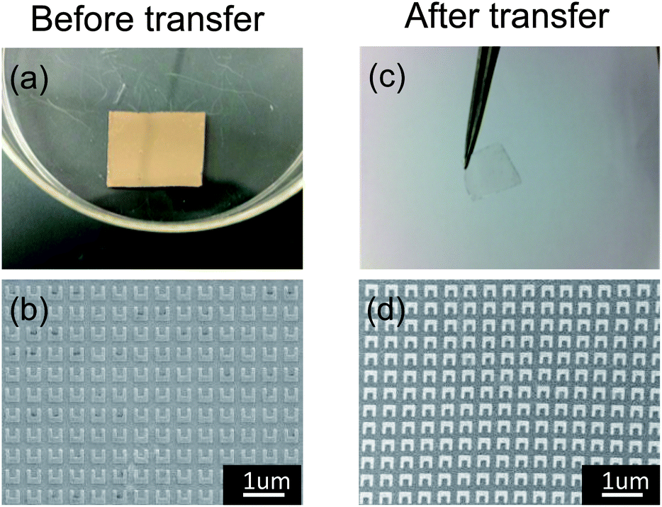 | ||
| Fig. 2 Metamaterials on a rigid substrate before transfer and on PDMS after transfer. (a) Photograph of Ni/SiO2/Si substrate with metamaterials fabricated on it. (b) SEM image of metamaterials on rigid substrate from (a). (c) Photograph of PDMS with metamaterials on it after transfer. (d) SEM image of metamaterials on PDMS substrate from (c). Note: SEM images (b) and (d) are from the same pattern. | ||
Apart from the structures of the pattern, the optical properties of the metamaterials on PDMS also need to be checked in order to make sure the optical properties are maintained after transfer. The electric resonance of SRRs arises from the dipole formation in the arms and bottom bar with any polarization, while the appearance of magnetic resonance is due to the circulating current excited when the polarization is parallel to the gap. Here we measure the transmission spectrum with a microspectrophotometer (Craic 20). Both electric and magnetic resonances are supposed to be present because the light source we use is unpolarized. As Fig. 3a shows, we measure several structures with different arm widths (the whole structure size is shrunk in accordance with the width). For 30 nm width, both electric and magnetic resonance can be observed; for 40 nm, 50 nm and 60 nm width, electric resonance could be observed which red-shifted with increased size, while the magnetic resonance of these sizes was beyond our measurement limit. Compared with the same structures fabricated on PEN in our previous study,20 the resonance wavelength in PDMS is red-shifted, for example, the electric and magnetic resonance wavelengths with 30 nm arm width are 653 nm and 902 nm on PEN, respectively, and 780 nm and 1302 nm on PDMS, respectively. This red-shift can be explained by the fact that the PDMS exhibits a higher surrounding refractive index than air. In the meantime, filling in the gap introduces a higher capacitance, which induces a magnetic resonance red-shift based on ωLC = (LC)−1/2. In order to verify this conclusion, we simulated the transmission of SRRs embedded in PDMS with finite-difference time domain (FDTD) based on MEEP codes as shown in Fig. 3b using a constant refractive index of PDMS.48,49 In our simulation, the calculation region is surrounded by periodic boundary conditions on four cross section sides, and perfectly matched layers (PML) below and above the metamaterials’ element. Polarized plane wave excitation normally impinges the structure from the substrate side. A mesh size of 0.2 nm is used for the metal metamaterials and small gaps. The optical constant of gold is determined with the Drude–Lorentz model, and the refractive index of PDMS is assumed to be a constant of 1.4. The result shows that for the same size, the simulated electric and magnetic resonances in PDMS are red-shifted compared with the simulation on PEN as shown in ref. 20. The deviation of experimental data (Fig. 3a) and simulation results (Fig. 3b) may be caused by the slight deviation of the real structures’ parameters from the parameters we designed.
 | ||
| Fig. 3 Experimental and simulated transmission of metamaterials embedded in PDMS. (a) Experimental transmission spectra of SRRs with different arm widths embedded in PDMS. (b) Simulation transmission spectra of different size SRRs embedded in PDMS. Note: the whole SRR size is shrunk according the arm width. | ||
The SRR metamaterials embedded in PDMS can serve as very simple, convenient and effective SERS-active substrates by covering the PDMS on the surface with analytes of interest. Here we take 2-naphthalenethiol on a gold surface as a demonstration. The Raman measurement was conducted using a micro-Raman spectrometer (Horiba-JY T64000) with a 785 nm solid state laser as the excitation source. The excitation power is fixed at 2.6 mW and a 50× objective is used to collect the backscattering signal. Fig. 4a shows configuration 1, a monolayer of 2-naphthalenethiol is formed on the Au film due to thiol–Au bonding. The Au film is deposited on a silicon wafer by thermal evaporation. The corresponding Raman signal of configuration 1 is shown in Fig. 4e (black curve). No Raman signal can be detected when 2-naphthalenethiol is attached to a Au film, suggesting that the Au film by thermal evaporation is too smooth to be SERS-active. However, when we cover our metamaterials embedded in PDMS onto the top surface of the previous Au film subsequently, as shown in configuration 2 (Fig. 4b), a strong Raman signal can be achieved as shown in Fig. 4e (green curve). Compared to the signal due to the 2-naphthalenethiol powder (blue curve), many characteristic Raman modes can be identified, such as the 1379 cm−1 Raman shift due to a ring stretching mode, 764 cm−1 and 514 cm−1 due to ring deformation modes, and 1022 cm−1 shift due to C–H bending modes.50 We can also observe the corresponding Raman modes of the PDMS polymer (red curve) with Raman shifts of ∼489 cm−1 and 710 cm−1, which correspond to symmetric Si–O–Si stretching and symmetric Si–C stretching vibrational modes.51 For the configuration 2 measurement, the SRR size we used is 30 nm bar width. This is because the resonance wavelength of 30 nm bar width SRRs is around 780 nm, which is in close resonance with the excitation laser (785 nm), thus a higher Raman signal is produced. Other SRR sizes such as 40 nm and 50 nm can also give a SERS signal, but with lower signal intensity (thus not shown here). We simply place the PDMS onto the Au surface directly; the PDMS can adhere to the Au film fairly tightly due to van der Waals interactions and thus guarantee that the metamaterials are close enough to the 2-naphthalenethiol residing on the Au film. In addition, the PDMS is thin and transparent, therefore it imposes a negligible effect to the spectroscopic measurements.
 | ||
| Fig. 4 Raman spectra of 2-naphthalenethiol in different configurations. (a) A 2-NAT monolayer on Au film (60 nm), 2-NAT refers to 2-naphthalenethiol molecules. (b) PDMS with embedded metamaterials covers on Au surface with 2-NAT attached, PDMS-MMs refers to PDMS-metamaterials. (c) A 2-NAT monolayer is formed on the SRRs’ top surface. (d) PDMS-SRRs with a 2-NAT monolayer on the top surface cover on a clean Au film. (e) and (f) are the Raman spectra of the different configurations. Note: the vertical axis scale bar is different for (e) and (f). | ||
Comparing the Raman signals of configurations 1 and 2, we can conclude that the metamaterials embedded in PDMS play a key role in enhancing the SERS signal. We hypothesize that two enhancement pathways are responsible for the enormous enhanced Raman signal. The first is that the SRR metamaterials themselves can generate hotspots sustaining the SERS signal.20 Secondly, the coupling between the metamaterials and the Au film provides a more intense localized electric field to enhance the Raman signal further.36,37 In order to investigate the mechanism, we designed two more configurations. Configuration 3 (Fig. 4c) shows that a 2-naphthalenethiol monolayer is formed on the SRRs’ surface; there is no 2-naphthalenethiol on PDMS because 2-naphthalenethiol can only bind to a Au surface. The characteristic Raman modes of 2-naphthalenethiol in configuration 3 can be observed (Fig. 4f, red curve) though the signal intensity is weaker than that of configuration 2 (Fig. 4f, green curve). The SERS of configuration 3 is purely from the metamaterials embedded in PDMS. Subsequently, after placing the chip from configuration 3 onto a bare Au film to construct configuration 4 (Fig. 4d), the corresponding Raman signal in Fig. 4f (blue curve) is much stronger than that of configuration 3, revealing that the coupling between the metamaterials and the Au film further enhances the Raman signal significantly. This sandwich picture is similar to the interpretation of Leveque et al.,52 in which the incident laser excites the electric mode of the SRRs and the surface plasmon polariton (SPP) of the metal film. The coupling of the electric mode and SPP concentrates the electromagnetic field in the gap between SRRs and metal film when the SRRs are close to the metal surface. In this situation, the Raman signal of 2-naphthalenethiol molecules localized in the gap can be enhanced dramatically. The enhancement factor can be calculated by  ,53 where ISERS and Ipowder are the Raman intensities for the SERS sample and a normal powder sample, respectively, and NSERS and Npowder are the amount of molecules probed in the measurement of the SERS sample and powder sample, respectively. Based on the ring–ring stretching Raman mode of 2-naphthalenethiol at 1379 cm−1, the enhancement factors of configurations 1–4 are 0, 4.9 × 10⁶, 3.4 × 10⁵ and 8.6 × 10⁶, respectively. It was noted that for configurations 3 and 4, the arrangement of metamaterials and Au film are the same. The only difference is the position and amount of the 2-naphthalenethiol molecules. The higher EF of configuration 4 suggests that the molecules outside the gap between the SRRs and Au film contribute less than the molecules localized in the gap.
We further conducted the simulation of the local electrical field distribution for the configurations described above to understand the enhancement mechanism. Previously, the coupling of nanoparticles and metal films has been studied,52,54 concluding that the coupling is highly dependent on the distance between the nanoparticles and the metal film. However, in our measurement the PDMS film was put on the Au surface without additional control. As a result, the bonding between the PDMS film and the Au surface is only via van der Waals interactions. In our simulations, we treat the distance as 1 nm and conduct the simulation using finite difference time domain (FDTD) approaches. This near-field is simulated at the excitation laser wavelength, namely 785 nm. Fig. 5a and 5b schematically show the configuration without and with Au underneath, respectively. Fig. 5a-1 and 5a-2 are the cross sectional view and the top view, respectively, as the axis indicates. The hotspots localized on the SRRs’ surface are responsible for the SERS effect in configuration 3 (Fig. 4c) in which the molecules are on the SRRs’ surface. When we place the metamaterials embedded in PDMS onto a Au film, Fig. 5b-1 shows that the electromagnetic field in the gap between the SRRs and the Au film is quite strong. The zoomed-in image (Fig. 5b-2) clearly shows that the dramatic Raman signal enhancement in configurations 2 and 4 should be attributed to the strong electromagnetic field localized in the gap. The field distributions of surface 1 and surface 2 (Fig. 5b) are described in Fig. 5b-3 and 5b-4, which corresponds to the molecules’ location in configurations 2 and 4, respectively. The average electric field is obtained according to the 2-naphthalenethiol molecules’ location, which means we only average the SRRs’ top surface for configurations 3 and 4, while we average the whole of the Au film surface for configuration 2. Table 1 summarizes the simulated and experimental enhancement factors of different SERS configurations. The enhancement factor is proportional to |ESERS|4/|Eincidence|4, but the exact value cannot be estimated with this formula because we have to consider the mismatch between the incidence light wavelength, resonance frequency and Raman radiation frequency. However, the trend of the simulated data agrees well with our experimental results. As we demonstrate here regarding the coupling between metamaterials and Au film, the nanostructures embedded in PDMS also can be placed onto other substrate materials to investigate their interactions, making this system a representative model for the study of particle–film interactions. In addition, from configuration 3 in Fig. 4, we can see that the metamaterials themselves can also enhance the Raman signal. This means that a flexible SERS substrate is not only limited to a metal surface, and PDMS–metamaterials can potentially be applied to some non-metal surfaces.
 | ||
| Fig. 5 Electric field simulation. (a) SRR embedded in PDMS. (b) SRR embedded in a PDMS layer on a Au film. (a-1) Electric field distribution of configuration (a) in cross section view. (a-2) Electric field distribution of configuration (a) in top view. (b-1) Electric field distribution of configuration (b) in cross section view. (b-2) Zoomed-in image of the gap between the Au film and SRR. (b-3) and (b-4) are the electric field distribution on surfaces 1 and 2 as indicated in (b), respectively. Note: the gap between the SRR and Au film is 1 nm and the color bar value indicates |E|4. | ||
| System | Calculation enhancement factor |ESERS|4/|Eincidence|4 | Experimental enhancement factor
|
|---|---|---|
| a The integration region is the Au film surface. b The integration region is the SRR top surface. | ||
| Configuration 2 | 2.9 × 10⁵a | 4.9 × 10⁶ |
| Configuration 3 | 1.0 × 10³b | 3.4 × 10⁵ |
| Configuration 4 | 1.8 × 10⁶b | 8.6 × 10⁶ |

Conclusion
We have shown a simple but effective Ni sacrificial layer assisted transfer method to fabricate visible–near IR metamaterials embedded into a flexible and transparent PDMS matrix. The optical properties are maintained after transfer to PDMS, with both electric and magnetic resonances of the metamaterials present. A convenient SERS strategy is demonstrated utilizing the metamaterials embedded in PDMS, in which SERS can be achieved by covering a Au film with a PDMS–metamaterials layer with the probed molecules residing on it. Our measurements in a variety of configurations and simulation results reveal that the coupling of the metamaterials and the Au film is responsible for the dramatic Raman signal enhancement, which is even better than with metamaterials alone. The coupling study shows the potential of our system as a representative model to investigate the interaction between metamaterials or other plasmonic structures and substrate materials.Acknowledgements
The author Q.X. thanks the strong support from the Singapore National Research Foundation through a Fellowship grant (NRF-RF2009-06), the support from the Singapore Ministry of Education via two Tier 2 grants (MOE2011-T2-2-085 and MOE2011-T2-2-051), and very strong support from Nanyang Technological University via start-up grant (M58110061).Notes and references
- Z. Y. Fan, H. Razavi, J. W. Do, A. Moriwaki, O. Ergen, Y. L. Chueh, P. W. Leu, J. C. Ho, T. Takahashi, L. A. Reichertz, S. Neale, K. Yu, M. Wu, J. W. Ager and A. Javey, Nat. Mater., 2009, 8, 648–653 CrossRef CAS PubMed.
- G. H. Gelinck, H. E. A. Huitema, E. van Veenendaal, E. Cantatore, L. Schrijnemakers, J. B. P. H. van der Putten, T. C. T. Geuns, M. Beenhakkers, J. B. Giesbers, B.-H. Huisman, E. J. Meijer, E. M. Benito, F. J. Touwslager, A. W. Marsman, B. J. E. van Rens and D. M. de Leeuw, Nat. Mater., 2004, 3, 106–110 CrossRef CAS PubMed.
- M. C. McAlpine, H. Ahmad, D. W. Wang and J. R. Heath, Nat. Mater., 2007, 6, 379–384 CrossRef CAS PubMed.
- K. Takei, T. Takahashi, J. C. Ho, H. Ko, A. G. Gillies, P. W. Leu, R. S. Fearing and A. Javey, Nat. Mater., 2010, 9, 821–826 CrossRef CAS PubMed.
- Y. Liu and X. Zhang, Nanoscale, 2012, 4, 5277–5292 RSC.
- J. B. Pendry, D. Schurig and D. R. Smith, Science, 2006, 312, 1780–1782 CrossRef CAS PubMed.
- J. B. Pendry, Phys. Rev. Lett., 2000, 85, 3966–3969 CrossRef CAS.
- T. M. Grzegorczyk and J. A. Kong, J. Electromagn. Waves Appl., 2006, 20, 2053–2064 CrossRef PubMed.
- Y. Liu and X. Zhang, Chem. Soc. Rev., 2011, 40, 2494–2507 RSC.
- D. R. Smith, J. B. Pendry and M. C. K. Wiltshire, Science, 2004, 305, 788–792 CrossRef CAS PubMed.
- N. Fang, H. Lee, C. Sun and X. Zhang, Science, 2005, 308, 534–537 CrossRef CAS PubMed.
- D. Schurig, J. J. Mock, B. J. Justice, S. A. Cummer, J. B. Pendry, A. F. Starr and D. R. Smith, Science, 2006, 314, 977–980 CrossRef CAS PubMed.
- N. R. Han, Z. C. Chen, C. S. Lim, B. Ng and M. H. Hong, Opt. Express, 2011, 19, 6990–6998 CrossRef CAS PubMed.
- I. M. Pryce, Y. A. Kelaita, K. Aydin and H. A. Atwater, ACS Nano, 2011, 5, 8167–8174 CrossRef CAS PubMed.
- S. Aksu, M. Huang, A. Artar, A. A. Yanik, S. Selvarasah, M. R. Dokmeci and H. Altug, Adv. Mater., 2011, 23, 4422–4430 CrossRef CAS PubMed.
- I. M. Pryce, K. Aydin, Y. A. Kelaita, R. M. Briggs and H. A. Atwater, Nano Lett., 2010, 10, 4222–4227 CrossRef CAS PubMed.
- X. G. Peralta, M. C. Wanke, C. L. Arrington, J. D. Williams, I. Brener, A. Strikwerda, R. D. Averitt, W. J. Padilla, E. Smirnova, A. J. Taylor and J. F. O'Hara, Appl. Phys. Lett., 2009, 94, 161113 CrossRef.
- J. F. O'Hara, R. Singh, I. Brener, E. Smirnova, J. G. Han, A. J. Taylor and W. L. Zhang, Opt. Express, 2008, 16, 1786–1795 CrossRef.
- H. Tao, A. C. Strikwerda, K. Fan, C. M. Bingham, W. J. Padilla, X. Zhang and R. D. Averitt, J. Phys. D: Appl. Phys., 2008, 41, 232004 CrossRef.
- X. L. Xu, B. Peng, D. H. Li, J. Zhang, L. M. Wong, Q. Zhang, S. J. Wang and Q. H. Xiong, Nano Lett., 2011, 11, 3232–3238 CrossRef CAS PubMed.
- D. L. Jeanmaire and R. P. Vanduyne, J. Electroanal. Chem., 1977, 84, 1–20 CrossRef CAS.
- M. Moskovits, Rev. Mod. Phys., 1985, 57, 783–826 CrossRef CAS.
- M. Hu, F. S. Ou, W. Wu, I. Naumov, X. M. Li, A. M. Bratkovsky, R. S. Williams and Z. Y. Li, J. Am. Chem. Soc., 2010, 132, 12820–12822 CrossRef CAS PubMed.
- H. You, Y. Ji, L. Wang, S. Yang, Z. Yang, J. Fang, X. Song and B. Ding, J. Mater. Chem., 2012, 22, 1998 RSC.
- J. X. Fang, S. Y. Du, S. Lebedkin, Z. Y. Li, R. Kruk, M. Kappes and H. Hahn, Nano Lett., 2010, 10, 5006–5013 CrossRef CAS PubMed.
- S. Dodson, M. Haggui, R. Bachelot, J. Plain, S. Li and Q. H. Xiong, J. Phys. Chem. Lett., 2013, 4, 496–501 CrossRef CAS.
- D. S. Wang and M. Kerker, Phys. Rev. B: Condens. Matter Mater. Phys., 1981, 24, 1777–1790 CrossRef CAS.
- M. Fleischm, P. J. Hendra and A. j. Mcquilla, Chem. Phys. Lett., 1974, 26, 163–166 CrossRef.
- M. G. Albrecht and J. A. Creighton, J. Am. Chem. Soc., 1977, 99, 5215–5217 CrossRef CAS.
- M. D. Musick, C. D. Keating, L. A. Lyon, S. L. Botsko, D. J. Pena, W. D. Holliway, T. M. McEvoy, J. N. Richardson and M. J. Natan, Chem. Mater., 2000, 12, 2869–2881 CrossRef CAS.
- B. Peng, G. Y. Li, D. H. Li, S. Dodson, Q. Zhang, J. Zhang, Y. H. Lee, H. V. Demir, X. Y. Ling and Q. H. Xiong, ACS Nano, 2013, 7, 5993–6000 CrossRef CAS PubMed.
- C. Cao, J. Zhang, X. Wen, S. L. Dodson, N. T. Dao, L. M. Wong, S. Wang, S. Li, A. T. Phan and Q. H. Xiong, ACS Nano, 2013, 7, 7583–7591 CrossRef CAS PubMed.
- Y. C. Yeh, B. Creran and V. M. Rotello, Nanoscale, 2012, 4, 1871–1880 RSC.
- L. Zhang, C. Jiang and Z. Zhang, Nanoscale, 2013, 5, 3773–3779 RSC.
- G. Lu, H. Li and H. Zhang, Small, 2012, 8, 1336–1340 CrossRef CAS PubMed.
- I. Yoon, T. Kang, W. Choi, J. Kim, Y. Yoo, S. W. Joo, Q. H. Park, H. Ihee and B. Kim, J. Am. Chem. Soc., 2009, 131, 758–762 CrossRef CAS PubMed.
- J. W. Zheng, Y. G. Zhou, X. W. Li, L. Ji, T. H. Lu and R. A. Gu, Langmuir, 2003, 19, 632–636 CrossRef CAS.
- R. M. Stockle, Y. D. Suh, V. Deckert and R. Zenobi, Chem. Phys. Lett., 2000, 318, 131–136 CrossRef CAS.
- B. Pettinger, B. Ren, G. Picardi, R. Schuster and G. Ertl, Phys. Rev. Lett., 2004, 92, 096101 CrossRef.
- J. F. Li, Y. F. Huang, Y. Ding, Z. L. Yang, S. B. Li, X. S. Zhou, F. R. Fan, W. Zhang, Z. Y. Zhou, Y. Wu de, B. Ren, Z. L. Wang and Z. Q. Tian, Nature, 2010, 464, 392–395 CrossRef CAS PubMed.
- G. Lu, H. Li and H. Zhang, Chem. Commun., 2011, 47, 8560–8562 RSC.
- K. A. Willets and R. P. Van Duyne, Annu. Rev. Phys. Chem., 2007, 58, 267–297 CrossRef CAS PubMed.
- S. Linden, C. Enkrich, M. Wegener, J. F. Zhou, T. Koschny and C. M. Soukoulis, Science, 2004, 306, 1351–1353 CrossRef CAS PubMed.
- N. Katsarakis, T. Koschny, M. Kafesaki, E. N. Economou and C. M. Soukoulis, Appl. Phys. Lett., 2004, 84, 2943–2945 CrossRef CAS.
- A. Kumar, H. A. Biebuyck and G. M. Whitesides, Langmuir, 1994, 10, 1498–1511 CrossRef CAS.
- C. Luo, A. Govindaraju, J. Garra, T. Schneider, R. White, J. Currie and M. Paranjape, Sens. Actuators, A, 2004, 114, 123–128 CrossRef CAS PubMed.
- C. H. Lee, D. R. Kim and X. L. Zheng, Nano Lett., 2011, 11, 3435–3439 CrossRef CAS PubMed.
- Polymer Data Handbook, ed. J. E. Mark, Oxford University Press, 2009 Search PubMed.
- A. F. Oskooi, D. Roundy, M. Ibanescu, P. Bermel, J. D. Joannopoulos and S. G. Johnson, Comput. Phys. Commun., 2010, 181, 687–702 CrossRef CAS PubMed.
- R. A. Alvarez-Puebla, D. S. Dos Santos and R. F. Aroca, Analyst, 2004, 129, 1251–1256 RSC.
- S. C. Bae, H. Lee, Z. Q. Lin and S. Granick, Langmuir, 2005, 21, 5685–5688 CrossRef CAS PubMed.
- G. Leveque and O. J. F. Martin, Opt. Express, 2006, 14, 9971–9981 CrossRef.
- A. D. McFarland, M. A. Young, J. A. Dieringer and R. P. Van Duyne, J. Phys. Chem. B, 2005, 109, 11279–11285 CrossRef CAS PubMed.
- J. J. Mock, R. T. Hill, A. Degiron, S. Zauscher, A. Chilkoti and D. R. Smith, Nano Lett., 2008, 8, 2245–2252 CrossRef CAS PubMed.
| This journal is © The Royal Society of Chemistry 2014 |