 Open Access Article
 This Open Access Article is licensed under a Creative Commons Attribution-Non Commercial 3.0 Unported Licence
Photocatalysts with internal electric fields
Li
Li
,
Paul A.
Salvador
and
Gregory S.
Rohrer
*
Department of Materials Science and Engineering, Carnegie Mellon University, Pittsburgh, PA, USA. E-mail: gr20@andrew.cmu.edu; Fax: +1 412 268 7596; Tel: +1 412 268 2696
First published on 23rd September 2013
Abstract
The photocatalytic activity of materials for water splitting is limited by the recombination of photogenerated electron–hole pairs as well as the back-reaction of intermediate species. This review concentrates on the use of electric fields within catalyst particles to mitigate the effects of recombination and back-reaction and to increase photochemical reactivity. Internal electric fields in photocatalysts can arise from ferroelectric phenomena, p–n junctions, polar surface terminations, and polymorph junctions. The manipulation of internal fields through the creation of charged interfaces in hierarchically structured materials is a promising strategy for the design of improved photocatalysts.
1. Introduction
Heterogeneous photochemical reactions on semiconductor surfaces can be used to separate hydrogen from water or to degrade organic pollutants.1–4 Hydrogen is an attractive fuel because it has a high energy density and its combustion does not produce greenhouse gases. Furthermore, if sunlight can be used as the source of photons to promote the reaction, then the production and combustion of hydrogen could provide a sustainable energy cycle. Although a practical synthetic strategy has not yet been demonstrated, there have been extensive research efforts directed at finding catalysts for solar hydrogen production.5–14 Oxides represent one of the most important classes of photocatalysts and, therefore, there have been a number of recent reviews that have focused on photocatalytic water splitting using metal oxides and on the photochemical properties of oxide surfaces.6,15–21 In this review, we discuss some of the challenges associated with optimizing these photocatalysts, and focus on how internal fields can improve photocatalytic properties, as well as strategies to optimize their use in functional catalysts.Light-driven water splitting processes can be coarsely classified into one of two categories, which are schematically shown in Fig. 1 using the archetypical Pt–TiO2 materials system. The first is photoelectrolysis, which uses a photoelectrochemical cell, or PEC (see Fig. 1(a)), with Pt and TiO2 as examples of the two separated electrodes. The second is photocatalytic water splitting using colloidal suspensions of powdered catalysts, with TiO2 as the base and Pt as a surface co-catalyst (see Fig. 1(b)).11,22–24 The PEC has the advantage that the photogenerated electrons and holes are separated on the macroscale to different electrodes, decreasing recombination and increasing efficiency. Furthermore, hydrogen and oxygen are evolved in the different locations, diminishing the back reaction of intermediate chemical species and eliminating the need for gas separation.25,26 However, the cost of constructing long-lived and efficient PECs has been a significant barrier to implementation.
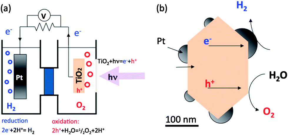 | ||
| Fig. 1 Simple schematic of (a) photoelectrochemical cell and (b) powdered photocatalyst (adapted from ref. 24). | ||
Powdered catalysts, on the other hand, have the potential to be produced at much lower costs through easily scalable processes. Note that the TiO2–Pt powdered catalyst can be thought of as a short-circuited version of the PEC; the reactions are spatially separated on the powdered catalyst, but on a much finer length scale than for the PEC. Compared to PECs, powdered catalysts have lower efficiencies. In other words, considering an equal amount of illumination, PECs generally produce more hydrogen. The particles that make up such powdered catalysts have nanoscale dimensions to increase total surface area and the number of available reaction sites. However, the small size of the particles brings several disadvantages. The first is that the interfacial space charge and band bending that tends to separate electrons and holes will not be present when the dimensions of the crystal are comparable to the width of the depletion layer.27 The second is that the photogenerated electrons and holes are spatially confined to be in close proximity. These two issues make electron–hole pairs more likely to recombine without reacting in small particles than in large particles. The third disadvantage is that the reaction products are also produced in close proximity (on the surface of the small particle) and this makes the back reaction of intermediate chemical species more likely. These three features lead to a loss of efficiency because of the combined effects of the recombination of photogenerated charge carriers and the back reaction of intermediate chemical species.6,18,28–33
Good catalysts balance the increase in density of reaction sites for high surface area powders with mechanisms to mitigate the increased recombination and back-reaction rates. Yet, significant room exists for improvement in the technology of photocatalytic water splitting with powdered photocatalysts, and this has motivated considerable research activity over the past decades. At this point, the highest reported quantum efficiency for splitting pure water with visible light and a powdered catalyst is 2.5% using a Cr/Rh-modified GaN/ZnO material system.7,34,35 (The quantum efficiency of a photocatalyst, defined as the ratio of the number of electrons that react to form the product to the number of incident photons, is one useful measure to compare photocatalysts.) In comparison, the maximum theoretical efficiency for water splitting using a semiconductor with a 2.5 eV band gap is 14%.36 Clearly, new directions are needed to improve catalyst efficiencies.
One concept that can be used to mitigate losses from recombination and back reaction is to use internal electric fields that will separate photogenerated carriers. Perhaps the best-known examples of these internal fields in photocatalysts are associated with interfaces, including the solution/photocatalyst interfaces,37,38 metal cocatalyst–photocatalyst junctions,39,40 and p–n junctions in composite photocatalysts.41,42 Internal fields at the solution/photocatalyst interface can be modified using different surface terminations,43–46 compositions or structures. They can also arise from step functions in the electrochemical levels associated with phase boundaries that are simpler to engineer than p–n junctions,47,48 including polymorph boundaries in compositionally uniform materials. Finally, they can arise in ferroelectric materials because of internal polar regions.16,49,50 When they have internal fields, powdered photocatalytic particles behave more like PECs.
This review will focus on recent studies of internal fields and their influence on photochemical reactions on oxide surfaces. We begin by reviewing some of the important materials requirements for photocatalysts and reactions on semiconductor surfaces. We will briefly cover the fundamentals of materials (§ 2) and solution photochemistry (§ 3) relevant to how internal fields improve photocatalytic performance and discuss how the size of phototcatalysts are coupled with these. We then review recent research exploring the effects of internal fields (§ 4) on photocatalytic water splitting that can arise from: (1) polarity associated with bulk ferroelectricity, and (2) electrochemical differences across phase boundaries, including p–n junctions, polar surface terminations on a single phase material, and phase boundaries in compositionally uniform materials. With regard to engineering at the nanoscale, the inclusion of internal fields adds several interesting challenges that point to improved performance through the use of hierarchically structured photocatalysts, or catalysts whose structures include multiple natural length scales. Where appropriate, we will give examples of these materials.
2. Materials requirements for photocatalysts
The materials most commonly used for water spitting are semiconductors, although there have been some novel catalysts developed by combining polymers with semiconductors.51–53 The overall mechanism for photocatalytic water splitting by a semiconductor (exemplified using TiO2–Pt) is illustrated schematically in Fig. 2.24,54 When the photocatalyst absorbs photons with energies that are greater than the bandgap, electrons are promoted to the conduction band and, if they reach the surface, are available for reduction reactions. Similarly, the remaining holes in the valence band are available for oxidation reactions. In the case of the n-type TiO2–Pt example, the electrons are active on the Pt surface and the holes on the TiO2 surface. Even from this simple picture, six intrinsic materials requirements can be articulated for any photocatalyst, originally done so by Morrison.36 | ||
| Fig. 2 Schematic representation of water photoelectrolysis using illuminated titania semiconductor electrode (adapted from ref. 24). | ||
First, the absorption spectrum of the photocatalyst must have an adequate overlap with the solar spectrum, and this is mostly controlled by the bandgap. The bandgap must obviously be larger than the energy needed to split water (Es = 1.23 eV) plus any overpotential for the surface reactions. It is not possible for water splitting to recover all of the energy in the solar spectrum for three main reasons. First, that part of the solar spectrum with energies less than Es will not split water. Second, when light with an energy greater than Es is absorbed, the excess energy is not recovered. Finally, in most practical cases the absorption edge of the catalyst is greater than Es and energy below this edge is also not recovered. Based on these considerations, it has been estimated that the maximum efficiency for water splitting is 14% for a catalyst with a single bandgap energy of 2.5 eV.36
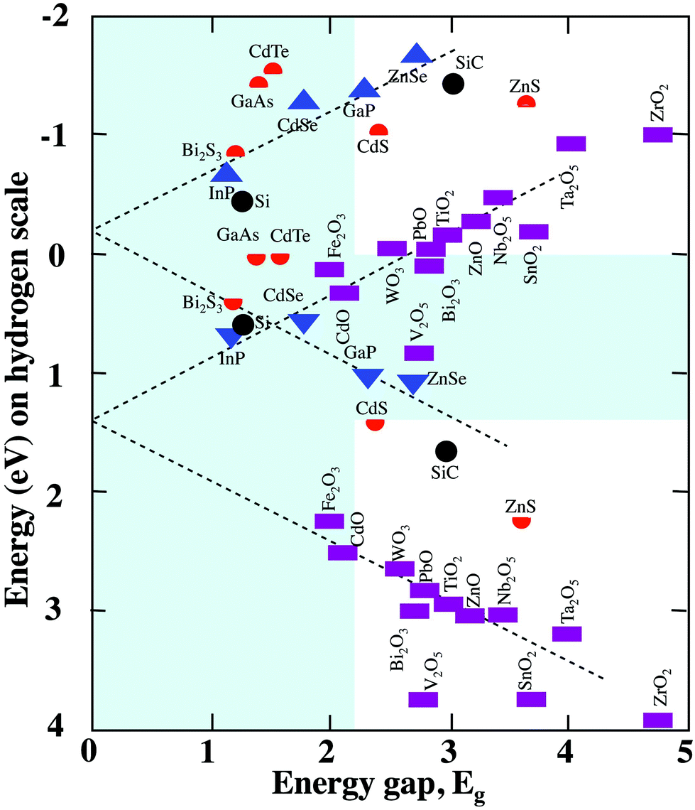
Second, the conduction band edge must be at a higher energy than the reduction potential of hydrogen (plus overpotentials) and the valence band edge must be lower than the oxidation potential of water (plus overpotentials). The band edge positions (relative to the hydrogen scale) of some semiconductors are plotted in Fig. 3 as a function of their bandgap energies.36 Note, for any pair of points for a single material, the upper (lower) point indicates the conduction (valence) band edge. The water redox levels are at 0 and 1.23 eV and useful band edge positions are represented as those falling outside the shaded area between these values. Overpotentials are not included in the shaded area because they vary with material and reaction; as such these are the minimal requirements for reaction. Being inside the shaded area rules one out as a candidate. One can safely add the overpotentials to the band gap requirement; assuming that the overpotentials add to roughly 1 eV, then a semiconductor's band gap must fall outside of the shaded region from 0 to 2.23 eV to be active for water splitting. Therefore, useful semiconductors for photocatalysts will be those having both band edges outside the shaded region. While there are a limited number of binary compounds that meet these criteria,6,19,55 suitable compounds may be found among ternary, quaternary, or more complex compounds. So-called Z-scheme multi-phase catalysts can be designed from slightly narrower gap materials that have one compound well suited for reduction and the other well suited for oxidation, and such materials have been reviewed elsewhere.6,20,55
 | ||
| Fig. 3 Schematic representation of the band gap energies and band positions for some semiconductors (adapted from ref. 36). | ||
A third materials requirement is that redox reactions are catalytically activated to reduce the overpotientials. There are generally energy barriers for the transfer of an electron or a hole from the surface to species adsorbed from solution. These barriers represent energy that is irreversibly lost in the reaction, so anything that lowers the barrier will promote the reaction. The most common example is the addition of Pt to titania (or other oxides) to promote the reduction reaction.29 In other cases, RuO2 is added to promote the oxidation reaction.6 The use of co-catalysts to reduce overpotentials is just one example of how composites of multiple phases can be used to produce improved catalysts. Also, co-catalysts are generally much smaller in size than the base catalyst,39 because they are more active than the base catalyst and are not (generally) involved in light absorption. This is one clear example of how creating multiple length scales in a single catalytic system leads to improved performance.
A fourth materials requirement is that the catalyst does not dissolve, corrode, or reversibly change during use. There are a number of photocatalysts that have high visible light activity for water splitting but, because of decomposition, lose their photocatalytic activity in a short time.56,57 This may not affect short term laboratory studies, but it is a serious practical concern for the application of photocatalysts. This particular materials requirement is not easily satisfied, as many oxides are slightly water soluble and many ternary oxides can leach alkali and alkaline earth components into water. The remarkable stability of titania is one of the reasons for its common use as a photocatalyst. The lower stability of ferroelectric BaTiO3 in photochemical environments has led to the use of TiO2-coated BaTiO3.58–60 Through proper engineering of the heterostructured particles, including hierarchical structures, the composites can be made to perform better than either of the parent phases alone.58–60
The fifth and sixth intrinsic materials requirements are that charge carriers be spatially separated to reduce recombination losses and the oxidation and reduction half-cell reactions be spatially separated to reduce the back-reaction of intermediates. Any internal electrochemical field present within the crystal can be used to separate charges, and doing so is the start to satisfying both of these materials requirements. Internal fields may arise from electrochemical potential differences at the junctions of the semiconductor with other solids or solutions, or from the polarization in a ferroelectric material. These mechanisms will be discussed in more detail in § 4.
It should be noted that there are also extrinsic aspects of the catalyst that affect the reaction rates/efficiencies. In this context, the term extrinsic refers to characteristics of the material that are inherited from the processing and can be varied in the synthesis. The principle extrinsic factors are particle size, particle shape, polymorphic form, crystallinity, and non-equilibrium defect structures. For composite catalysts, similar issues related to charge transfer across the interface must also be considered.
Particle size is important because it controls the surface-to-volume ratio. The volume of the catalyst is important for the generation and separation of electron–hole pairs, while the surface is essential for carrying out the heterogeneous reaction. Nanoscale catalysts have the advantage of having large surface areas and, therefore, a larger number of active sites per volume (or mass) of catalyst to promote the reaction. Smaller particle sizes also mean shorter distances for photogenerated charge carriers to migrate before reaching surface reaction sites, which can improve performance.6,61,62 However, smaller particle sizes mean that the electron–hole pairs are confined to a smaller space and, therefore, should be more likely to collide and recombine. As a result, electron–hole recombination increases inversely with particle volume.24 Clearly the size of an individual particle must be chosen as a compromise between the positive influence of having more reactive sites and the negative influence of increased recombination. Alternatively, one must develop catalyst structures that can exploit the nanoscale improvements while avoiding their detrimental effects. Hierarchically structured catalysts, which combine microscale and nanoscale lengths in powdered catalysts, offer a potential method to simultaneously optimize both requirements. Some examples will be described in § 4.
In addition to the geometric effects, the electronic nature of the catalyst also changes when particles become small enough, and this can also influence reactivity. For example, when the particle size is smaller than twice the width of the surface space charge region present for a bulk material, which is not larger than two times 100 nm for TiO2,63 the bands do not completely relax to the bulk level. Assuming the potential of an electron at the surface is the same, as is shown in Fig. 4, the potential drop and electric field across the space charge region are smaller for small particles.64 This should couple directly to the proximity effect, and the recombination rate for photogenerated charge carriers increases with the decrease of particle size in the nano-range. Another electronic effect known for small particles is an increase in the bandgap because of quantum confinement.65–67 With regards to photocatalysis, a larger bandgap means less solar energy is harvested, but it may also mean that the band edge positions are modified favorably. Consideration of the electronic features argues that, for most photocatalysts, particles should be large enough to take advantage of band bending, but no larger. In other words, a particle size comparable to twice the width of the space charge region would be appropriate. As before, a balance must be struck between using larger particles for better separation of photogenerated carriers and using smaller particles for maximizing reactive site densities and this can be achieved through hierarchically structured photocatalysts.
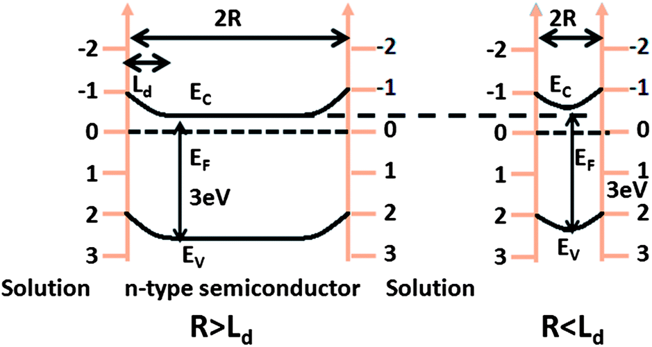 | ||
| Fig. 4 Band structure of an n-type semiconductor in solution with different particle sizes. (a) R is greater than the space charge width and (b) R is less than the space charge width. EV is the valence band edge, EF is the Fermi level, EC is the conduction band edge, Ld is the space charge width (adapted from ref. 64). | ||
The effects of particle shape on photochemistry have also been actively investigated.46 It has been demonstrated that some crystal orientations are much more reactive than others and, because of this, one might infer that the overall reactivity could be related to the particle shape.46,68,69 For example, Fig. 5 shows SEM micrographs of faceted SrTiO3 crystals after the photochemical reduction of silver. The silver preferentially reacts on the (100) faces.70 Similar phenomena have been observed for rutile, anatase, and BiVO4.71–73 The differences have been correlated to systematic differences in the surface electrochemical potentials, including solid and solution contributions, or anisotropic transport properties along different directions. The former may indicate different internal fields present normal to the different surface orientations. Furthermore, the reactivities of different facets have been correlated to the relative size of faceted particles, indicating the shape and size together play a role in what carrier/reaction is preferred on different surfaces. Because this area has not been thoroughly investigated, it may represent a relatively untapped parameter for designing nanoscale catalysts that overcome some of the inherent limitations imposed by particle size effects discussed above for isotropic particles.
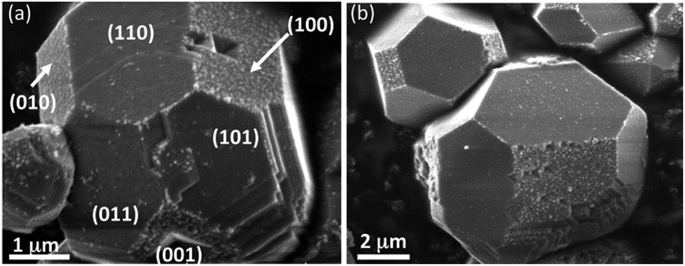 | ||
| Fig. 5 SEM images of faceted SrTiO3 crystals after exposure to UV light in an aqueous AgNO3 solution. The white contrast on the crystal facets corresponds to silver containing deposits produced by the photochemical reduction reaction.70 | ||
Many oxides can be crystallized in different polymorphs that are metastable in service. TiO2, the most commonly used photocatalyst, has three naturally occurring crystalline polymorphs: anatase, rutile, and brookite; it can also be easily synthesized in structures such as TiO2–B or as an amorphous solid. Anatase and rutile are generally regarded to be photocatalytic whereas brookite is not.28,74 Anatase is reported to have a higher photocatalytic activity than rutile because of a lower rate of charge carrier recombination and more negative conduction band position.75,76 However, rutile displays the same effective photocatalytic decomposition of pollutants.77 It has been reported that mixtures of rutile and anatase exhibit enhanced photocatalytic activity compared to the same isolated materials. This has been explained by increased light absorption in rutile and the transfer of photogenerated electrons to trapping sites in anatase, which decreases the recombination of photogenerated charge carriers.78 Examples of polymorphic composites are described in more detail in § 4.2.3.
The degree of crystallinity and the defect content also affect the charge carrier recombination rate, bulk transport, and ultimately the reactivity of the material. In general, almost all typical crystal defects—grain boundaries, dislocations, native point defects, and substitutional impurities—are expected to promote the scattering and recombination of carriers. As such, improved crystallinity, defined as having fewer non-equilibrium defects in the photocatalyst, should lead to improved bulk transport and reduced recombination.6 On the other hand, low-temperature and other non-equilibrium preparation routes for the fabrication of metastable or nanophase materials may result in large numbers of defects in otherwise highly reactive systems. Using annealing methods to improve crystallinity can also lead to coarsening or phase transformation, rendering optimal catalyst design in single-phase materials challenging. For example, because the transformation temperature from anatase to rutile in TiO2 is in the range of 500 °C to 600 °C, at the low-end of the temperature range expected to recover the maximum crystal quality in anatase. Thus, annealing to increase crystallinity of the reactive anatase TiO2 can also lead to transformation to the lower reactivity rutile polymorph.79–81 Again, heterostructured catalysts can offer improved design and better processing windows as anatase particles (and other metastable polymorphs) are known to have improved thermal stability on certain types of substrates.59
Many of the above-described extrinsic factors also are relevant to the phase boundary in multi-phase catalysts. Even for the TiO2–Pt powdered catalysts, charge transfer at the TiO2/Pt interface should be uninhibited, and the interface quality (bonding) will strongly affect this. As with the bulk crystallinity, increased annealing temperatures promote strong interfacial bonding, but come at the expense of coarsening in the co-catalysts (or smaller length scale material).59 As such, processing windows must be optimized to increase the interface quality to improve charge transfer while maintaining appropriate particles size/surface coverage, as demonstrated for hierarchically structure catalysts, such as nanostructured TiO2 shells on microcrysalline BaTiO3 cores.59
3. Photochemistry on the semiconductor surface
3.1. Energy levels in the semiconductor and solution
From the discussion of materials requirements in § 2, it becomes obvious that we need a system of evaluating the energies of electrons in solids. Specifically, we need to know the energies levels and their relation to redox couples. Throughout this paper, we shall use the convention that the zero of energy is defined as the hydrogen redox reaction at the normal hydrogen electrode, as defined in Fig. 6. The energy level has been determined to be 4.5 eV lower than an electron at the vacuum level.82–84 By convention, the vacuum level is taken to be negative with respect to the hydrogen ionization reaction.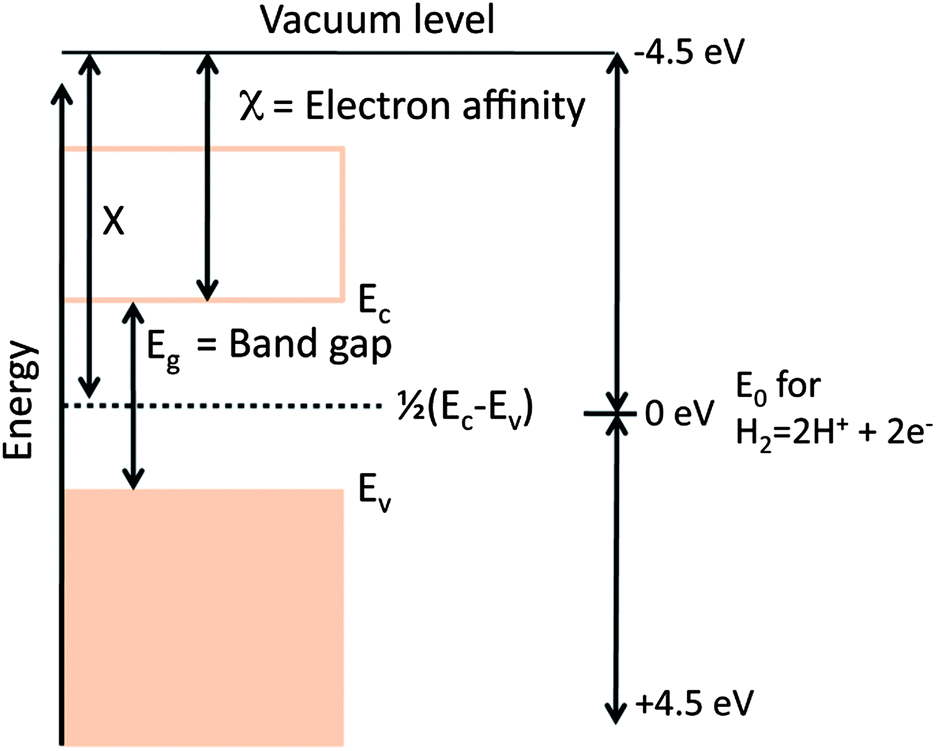 | ||
| Fig. 6 Schematic representation of some fundamental semiconductor concepts used for photochemical reactions (Ec is conduction band, Ev valence band, X is the Sanderson electronegativity of the solid, E0 the energy of a free electron at the H2 redox potential). | ||
The semiconductor given in Fig. 6 is shown in the flat band configuration, which simply means that electron potential at the surface and in the bulk are identical (i.e., there is no band banding in the semiconductor). While the bandgaps of materials are often known from optical experiments, the conduction band edge is more difficult to determine experimentally. However, when the band gap (Eg) is known, there is a simple way to approximate the energy level of the conduction band edge (Ec) that was originally proposed by Butler and Ginley.85 If X is the Sanderson electronegativity of the solid (the energy difference between the vacuum level and the midgap position of the semiconductor), which is defined as the geometric mean of the Mulliken electronegativities the atoms, then Ec is defined as:
| −Ec = 4.5 eV − X + 1/2Eg. |
The Mulliken electronegativity of an atom is the average of the first ionization energy of the metal and the atomic electron affinity of the anion. As an example, the ionization energies of Ti and O are 6.83 eV and 13.62 eV, respectively, and the electron affinities are for Ti and O are 0.083 eV and 1.46 eV, respectively. The Mulliken electronegativies for Ti and O are therefore 3.45 eV and 7.54 eV, respectively. This leads to a Sanderson electronegativity of 5.8 eV and, assuming a band gap of 3.0 eV, the TiO2 flat band potential is 0.2 eV higher (more negative) than the hydrogen redox reaction.36 We are reminded of the importance of Ec and Eg in Fig. 2, which together determine whether the band edges are at appropriate levels for photocatalytic water splitting. Internal fields, the focus of this review, determine which type of carriers is preferentially shuttled to the surface.
3.2. Charge carrier redistribution near the surface for the semiconductor
Three primary effects cause charge carrier redistribution in the near surface region of the semiconductor. The first effect arises because of the termination of the bonding network at the surface, which causes the electronic states at the semiconductor surface to differ from those of the bulk. This can lead to a redistribution of mobile charge as the surface attracts specific carrier types in different populations than the bulk. Moreover, the nature of these surface states can be perturbed by interactions with the solution. Overall, these states are generally difficult to quantify, and are many times overwhelmed for solids in solutions by the other two effects.36 Most energy level diagrams of photocatalysts ignore these states. Even though they may be neglected on energy level diagrams, they may lead to states that impact the transfer of electrons across interfaces, affecting overall efficiencies.36The second effect arises from adsorption of ions. When a semiconductor is immersed in aqueous solutions, the surface chemisorbs charged species (H+ or OH−) in different populations, and this can change the pH of the water. Similarly, the charge adsorbed on the surface can be controlled by adjusting the pH of the solution. The pH value at which the concentrations of adsorbed H+ and OH− are equal is called the point of zero charge (PZC). The charge on the surface can either be screened within the semiconductor or within the solution itself, depending on which has the higher capacity to screen the charge. For insulators, screening always occurs in the solution Helmholtz and Guoy layers, as there are no available charges to screen the surface in the solid. For metals, charge adsorption is screened easily by mobile charges in the solid. For semiconductors, intermediate behavior may be observed. Assuming non-degenerate semiconductors with gaps wide enough to split water (≈1.5 to 2.5 eV) and concentrated electrolyte solutions typically used for photocatalytic experiments, the charge is screened in the Helmholtz layer. In this scenario, a voltage drop occurs in the Helmholtz layer that varies with pH away from the PZC. Assuming this to be true, then band diagrams can be drawn for the solid at the PZC for schematic purposes, and the Helmholtz voltage can be added later with no loss in generality. This is often done in papers on photocatalytic powders.
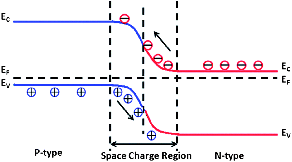
The third effect is related to electron transfer between the semiconductor and the electrolyte solution to achieve equilibrium between the electrochemical potential of electrons in the two materials. To achieve equilibrium, charge will exchange in a preferred direction between the solid and solution until the Fermi level of the semiconductor is equal to the redox potential of the solution, when charge transfer will be equal in both directions.38,86 Within the semiconductor, this exchange of charge is accomplished by the redistribution of mobile electrons or holes and the charge equilibration process leaves a region below of the surface that has an imbalance of charge, which is referred to as the space charge region. The local imbalance of charge causes the energy levels (potentials) of electrons (and holes) to spatially vary relative to a fixed reference level, a phenomenon referred to as band bending, because the energy levels of the bands also vary in potential relative to the fixed reference point. As a result, the physical and chemical properties of the space charge region are different from those in the bulk.17,87 This potential variation also leads to an internal electric field, which drives excess carriers (such as photogenerated ones) is opposite directions.
Three types of space charge regions can be identified and they are depicted schematically in Fig. 7 for the case of an n-type semiconductor.17,37,88 The case in Fig. 7(a) shows the initial (or flat band) condition, which occurs when there is no net charge transfer from the bulk to the surface or solution states. Assuming the Fermi energy of the solid is lower than the redox potential of the concentrated solution, electrons flow from the solution to the solid and lead to the situation depicted in Fig. 7(b). This is known as accumulation, because there is an excess of negative charge in the space charge region below the surface. This excess negative charge exists because the sheet of positive charge in the solution at the semiconductor surface causes a reduction in the energy levels of electrons in this region, compared to the bulk, and downward band bending. The spatial extent of the downward band bending is related to the electronic properties of the semiconductor and the required potential to be dropped across the space charge region, Vsc. If the Fermi energy of the solid is at a greater energy than the redox potential of the solution, the opposite will happen, as illustrated in Fig. 7(c). In this case, charge flows out of the solid, leaving ionized donors and positive charge in the space charge region below the surface, which is known as the depletion layer, and a sheet of negative charge in the solution at the surface of the semiconductor. The negative charge in the solution layer increases the relative potential of the electrons at the semiconductor compared to the bulk, and the bands bend upward as they relax to their equilibrium state. For the case of n-type oxides, these ionized donors are often oxygen vacancies.89,90 If there are not enough donors to compensate the charge and it is necessary to extract electrons from the valence band, then an inversion layer forms and the majority charge carrier at the surface changes from electrons to holes, as illustrated in Fig. 7(d).
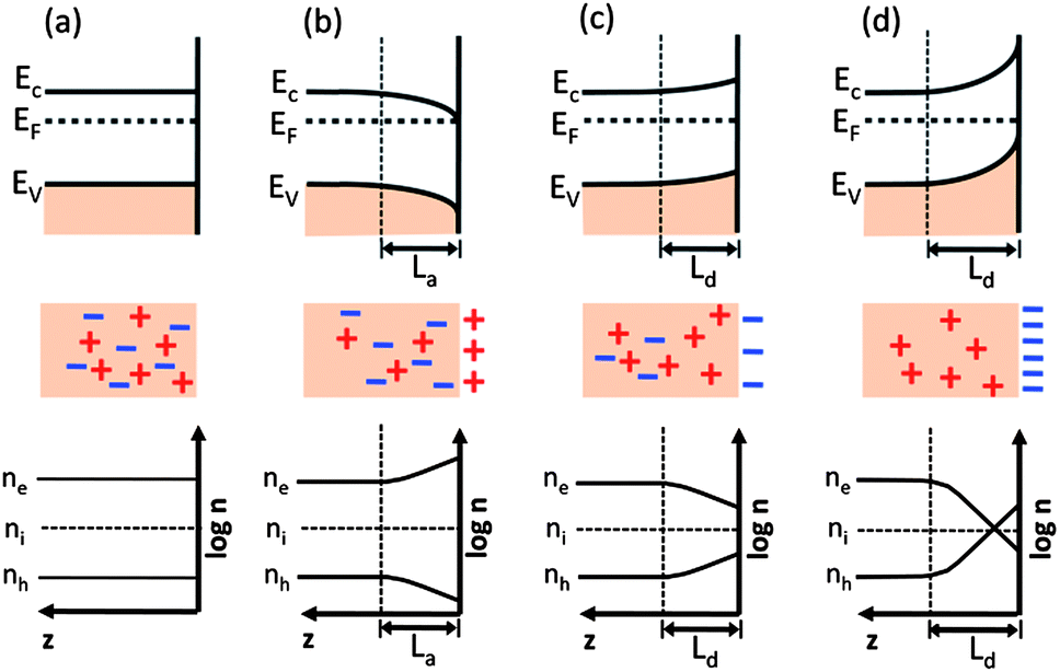 | ||
| Fig. 7 Schematic diagrams showing the energy levels and free charge carrier densities on (logarithmatic scale) from the n-type semiconductor surface to the bulk. (a) Flat band, (b) accumulation, (c) depletion, (d) inversion. The vertical dashed lines indicate the corresponding space charge region of thickness Ld or La. ne = free electron concentration; nh = free hole concentration; ni = intrinsic carrier concentration (adapted from ref. 17). | ||
Note that the existence of other potential drops at the solid/solution interface will modify the amount of charge transfer required to equilibrate the bulk electrochemical potentials. For example, if the Helmholtz voltage drop associated with ion adsorption is equal in magnitude but opposite in sign to the space charge potential Vsc for any of these cases, the bulk will be at the flat band condition. Also, applied potential differences (dropped across the solid/solution interface, which occur in most conditions described by the prior assumptions) can cause any of the cases of band bending (Fig. 7(a)–(d)) to occur.91
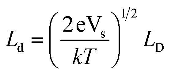
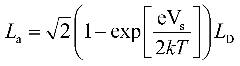
The subsurface space charge regions where the bands are bent from their equilibrium levels are important for photochemistry because when an electron–hole pair is created in this region, the charge carriers will move in opposite directions, with the electron proceeding to lower energy levels and the hole moving to higher energy levels. Obviously the dimensions of this region are important, especially in comparison to the absorption depth of the light and the size of the particle. The width of the space charge region in depletion (Ld) or accumulation (La) can be written as a function of the Debye length, LD, and the potential drop across the space charge region, Vsc (which depends on the factors described above).92 The Debye length is a characteristic of the material and depends on the dielectric constant and donor concentration according to eqn (1):92
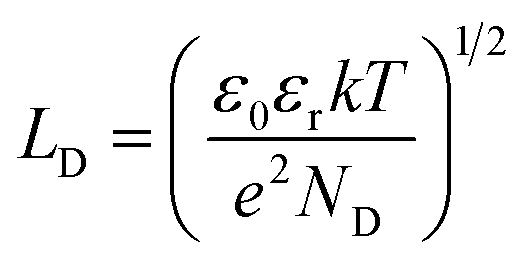 | (1) |
 | (2) |
 | (3) |
Using reasonable estimates for these parameters, the width of the depletion region in the materials of interest is in the range of 20 to 100 nm.17,36,93 Recall that when the size of an isotropic particle is less than or equal to twice the width of the space charge region, then the full extent of band bending cannot be sustained. Therefore, spatial separation arising from band bending is expected to be most effective in crystals with diameters greater than approximately 100 nm. The diminished effect of band bending is one of the reasons for enhanced recombination in catalyst particles with sizes less than 100 nm. Moreover, we would like to be able to control band-bending such that different regions of the surface experience different extents of band bending and promote different carriers to move to spatially different locations. This implies we must somehow cause the surface of effective photocatalysts to vary spatially. The most common method is to decorate the surface with a metallic co-catalyst, such as Pt for TiO2 photocatalysts. Note that simple co-catalyst additions have not yet resulted in technologically useful photocatalysts for water splitting.
3.3. Light absorption and charge transport
Important steps in photochemical reactions are the absorption of light and the transport of the photogenerated carriers. Understanding the materials parameters that quantify these processes is important for the design of semiconductor catalysts. The first important parameter is the absorption length of the incident light within the semiconductor. For radiation with energy greater than the absorption edge, the intensity of the incident radiation decreases exponentially with the distance of penetration. The characteristic absorption length is defined as the depth at which the incident intensity is reduced by a factor of 1/e. Using Beer's law,94,95 the absorption length, LP, is 1/α, where α is the absorption coefficient.The absorption coefficient is a material’s property that depends on the photon energy and increases steeply at the band gap energy. For example, at a photon energy of 3.4 eV, the absorption coefficient of rutile is 105 cm−1.93,96,97 This results in an absorption length of about 100 nm. In other words, most electron–hole pairs that are created by light absorption are created in the layer of material within 100 nm of the surface. It is important to compare this length scale to the width of the space charge region, wherein charge carriers are easily separated by the local field and are less likely to recombine.38,91 Those that are created deeper in the materials, where the bands are flat, are more likely to recombine. Recall that in the last section, it was noted that the space charge width within titania is in the range of 100 nm, comparable to the absorption depth.
The charge carrier diffusion length, or the distance that a charge carrier can diffuse before scattering and recombining, is denoted by Ldiff. If light is absorbed and carriers are created outside of the space charge region, but within the length Ldiff, there is chance that they can make it to the space charge region. Ldiff is simply the product of the charge carrier diffusion constant and the carrier lifetime. To utilize the most carriers for the reaction, the carrier lifetime and, therefore, the diffusion length, should be maximized. In general, the carrier lifetime increases with the perfection of the crystal.
Based on the above discussion, the ideal photocatalyst is a semiconductor in which the absorption length for the photons in the source of illumination is smaller than the width of space charge region plus the carrier diffusion length. In this case, all photogenerated charge carriers can be separated and have the potential to participate in the reaction.98 This also provides some guidance for the selection and design of nanoscale photocatalysts. To maximize light absorption and charge carrier separation, a semiconductor photocatalyst should have a size that is comparable to twice the size of the space charge region. It should be noted, however, that this may also reduce the surface area in a way that compromises any gains in yield. Therefore, improvement in photocatalyst design can be made by incorporating mechanisms to increase charge separation while maintaining high surface areas. Because these length scales are often at odds with one another, catalysts that have more than one length scale are of interest.
4. Internal fields
One of the important features limiting the efficiency of photocatalytic water splitting is the recombination of photogenerated charge carriers and the back reaction of intermediate chemical species that recombine to form water.26,99 As discussed above, space charges are effective in separating photogenerated carriers. However, in the cases above, the space charge characteristics are determined by the surface states and solution. Band bending can also be controlled by polar fields arising from ferroelectric domains, polar surface terminations, or heterojunctions between materials with different Fermi levels. With appropriate control of the built in fields, photogenerated charge carriers can be driven to the different facets of the crystal and thus separate the sites for oxidation and reduction reaction products.38,100–102 In this section, the sources of these electric fields and their influence on photochemistry will be discussed.4.1. Internal fields in ferroelectrics
A ferroelectric is an insulating material with two or more discrete stable (or metastable) states of nonzero electric polarization in zero applied electric field; this is referred to as spontaneous polarization.103 Ferroelectrics are non-centrosymmetric and the polarization occurs because the positive and negative charges have different centers of symmetry. Any two of the orientation states normally occur along indistinguishable crystallographic directions in the same crystal structure, differing only in the direction of the electric polarization vector.104 The polarization vector can be switched between these different orientation states with an applied electric field, which couples to the polarization and changes the relative energies of the states.103Spontaneous polarization in ferroelectrics arises from displacements of individual atoms or ions in the crystal structure.105 Perovskite oxides, with the general formula ABO3 (where A and B represents cationic elements) are among the most extensively studied ferroelectrics. BaTiO3, the first perovskite oxide compound identified as ferroelectric,103 is used here as an example to introduce polarization effects. Fig. 8(a)–(c) shows the crystal structure of BaTiO3 at different temperatures.106 At high temperatures (above 393 K), the crystal displays a cubic perovskite structure and there is no spontaneous polarization. When the temperature is below 393 K, but above 278 K, the Ti and Ba are shifted relative to the negatively charged O, which produces the polarization. The shift of atoms along the 〈100〉 direction leads to a change of crystal structure from cubic to tetragonal. When the temperature is below 278 K, the preferred displacement direction of atoms changes (from 〈100〉 to 〈110〉) and the structure converts to orthorhombic; below 183 K it converts to trigonal (with 〈111〉 displacements).107 The direction of atomic displacement determines the polarization direction. This critical transformation temperature from ferroelectric to non-ferroelectric is called the Curie temperature (TC).106,108 The high temperature phase that transforms to the ferroelectric below TC is described as paraelectric.107
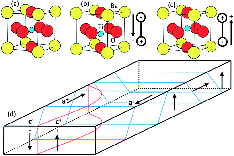 | ||
| Fig. 8 Atomic structure of BaTiO3 (a) in the cubic form above the Curie temperature; (b and c) below the Curie temperature, the position of the Ti(IV) atom in the center of the cell determines its dipole moment. Two of six possible orientations are illustrated; (d) domains are volumes of constant polarization separated by domain boundaries. The arrows show the polarization, the blue lines indicate 90° domain boundaries and the red lines indicate a 180° domain boundary. | ||
A depolarization field arises in spontaneously polarized domains which acts to neutralize the polarization by the flow of free charge within the crystal or the absorption of ions on the surface of the crystal from the surrounding medium.107,109 To minimize the depolarization field, the direction of the polarization varies from region to region within the crystal. Any region having a locally uniform polarization is called a domain; the boundary separating two domains is called a domain wall.16 The size of a domain is determined from the balance between the energy cost associated with forming the domain wall and the energy gain from reducing the depolarization field.104 Domain walls are often described by the angle formed between the polarization vectors on either side of the wall. In tetragonal BaTiO3, where the polarization directions are along the pseudocubic 〈100〉 directions, domain walls can be either 90° or 180°. The 90° and 180° domain walls are shown in Fig. 8(d). In this figure, “c+” and “c−” refers to domains with polarization vectors along (+) and (−) vertical z direction (vertical), respectively, while “a+” and “a−” represents domains along the horizontal a-axis.
For photocatalyst design, it is necessary to understand the influence of crystal size on the spontaneous polarization. It is known that the measured spontaneous polarization decreases with decreasing particle size in the nanoscale size range. Fig. 9 (ref. 110) show the size effect on spontaneous polarization for one of the common ferroelectrics, PbTiO3. Size dependent ferroelectric polarization is also observed for BaTiO3.111 It is reported that the ratio of the c-axis lattice constant to that of the a-axis decreases with decreasing particle size.112,113 The reduction in tetragonality means that the spontaneous polarization is decreased.110 As shown in Fig. 9, the ferroelectric polarization decreases for crystal sizes less than 100 nm. The ultimate size limit for the preservation of ferroelectric correlation in the ideal pervoskite is 2.6 nm.114,115 It has recently been reported that BaTiO3 nanocubes, prepared by a two-phase aqueous/organic synthesis procedure, can be switched at room temperature down to sizes as small as 10 nm; it was also shown that ferroelectric switching ultimately disappears in the size range of 5–10 nm.115 It should also be noted that the dielectric constant of ferroelectrics, which influences the width of the space charge region, also decreases significantly with grain size.116 Although the size dependence of the spontaneous polarization depends on the processing conditions, purity, and stoichiometry, it is best for photocatalytic applications to use particles greater than or equal to 100 nm so that the maximum intrinsic polarization is available to separate the photogenerated charge carriers.
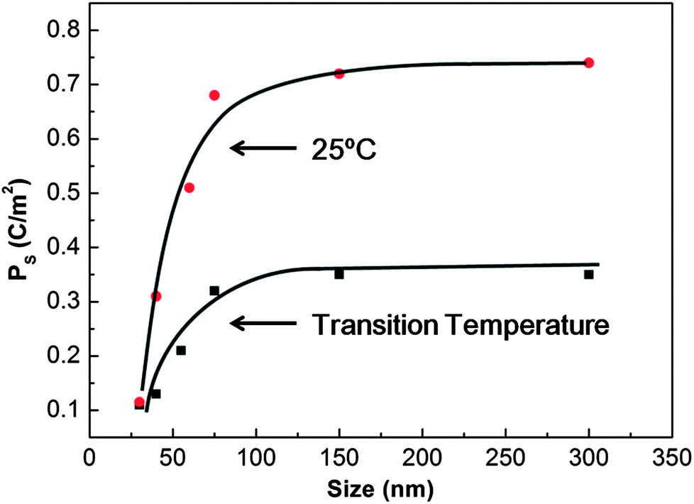 | ||
| Fig. 9 Variation of spontaneous polarization (Ps) at transition temperature and at room temperature (25 °C) with particle size for PbTiO3 (reproduced from ref. 110). | ||
The internal dipolar field within a ferroelectric creates charged surfaces that cause photogenerated carriers to move in opposite directions,117 which separates electrons and holes and causes oxidation and reduction products to be generated at different locations. In semiconducting ferroelectrics, the polarization can be screened by internal free charge carriers or defects in the bulk, which causes band bending, as depicted in Fig. 10 (in perfect insulators the potential drops linearly across the domain).118 The energy level diagrams are drawn with reference to the standard hydrogen electrode scale, assuming that the band gap of BaTiO3 is 3.2 eV,119,120 that the conduction band potential (EC) is close to 0 V,121 and that the semiconductor is n-type with donor states a few tenths of a volt below the conduction band edge that determine the Fermi level (EF).122 For a neutral domain (an a domain, as in Fig. 8), shown in Fig. 10(b), it is assumed that there will be a small amount of upward band bending in a solution with a pH near 7. For domains in which the positive end of the polarization vector points toward the surface (c+), a potential drops across the domain such that the surface is at a lower potential than the bulk. This potential drop reduces the band bending relative to the neutral surface and, depending on the magnitude of VS on the neutral surface and the ferroelectric potential drop, can even bend the bands downward, as shown in Fig. 10(a) (also it is assumed ferroelectric potential is screened by the accumulation layer of the semiconductor). In this case, the photogenerated electrons can easily reach the surface to react with the solution.123 The opposite occurs on negative domains (Fig. 10(c)), where the polarization increases the surface band bending and electrons are further depleted from the surface, with respect to the neutral surface. This obstructs the motion of photogenerated electrons to the surface but promotes the movement of photogenerated holes toward the surface where they can participate in the oxidation reaction. Because these different polarizations occur in spatially distinct domains, the electrons and holes are separated to different surfaces.
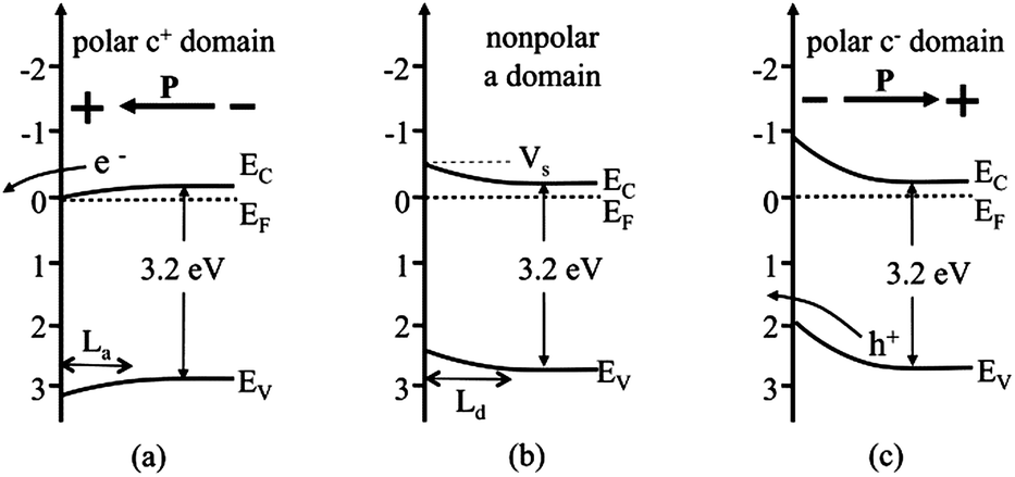 | ||
| Fig. 10 Energy level diagrams for BaTiO3 in aqueous solution, without illumination. The energies on the vertical axes are on the standard hydrogen electrode scale. EV is the valence band edge, EF is the Fermi level, EC is the conduction band edge, Vs is the surface potential, Ld is the width of the space charge layer in depletion, and La is the width of the space charge layer in accumulation. Band bending (a) for a c+ domain, (b) for an a domain, and (c) for a c− domain. | ||
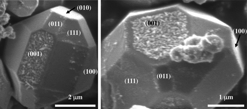
Many experiments have confirmed that dipolar fields in the ferroelectrics influence the locations of photochemical reactions.99,101,102 These experiments have employed so-called marker reactions that leave insoluble products at the reaction site to determine the correlation between polarization and reactivity. For example, Ag+ cations from a silver nitrate solution can be reduced to silver metal and Pb2+ cations from a lead acetate solution can be oxidized to form PbO2. The atomic force microscope (AFM) images in Fig. 11 show the surface of a BaTiO3 ceramic before (11(a and b)) and after (11(c and d)) using the surface to photocatalyze these reactions.63 The dark contrast in Fig. 11(b) corresponds to positive domains and the white contrast corresponds to negative domains. The image in Fig. 11(c) shows that silver was reduced on the positive domains and the image in 11(d) shows that lead is oxidized on negative domains, indicating that ferroelectric polarization determines the site of the redox reaction and separates the two half reactions to different domains. This same process can occur in microcrystals, as shown in Fig. 12.49 These images show that silver is preferentially reduced on {001} facets perpendicular to the direction of ferroelectric polarization.
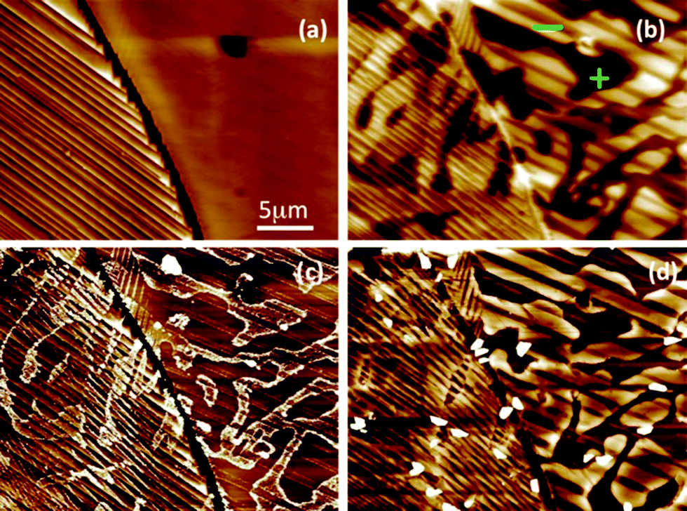 | ||
| Fig. 11 (a) Topographic AFM images of BaTiO3 surface before reaction and (b), a surface potential image recorded at the same time. (c) Topographic image after reaction in a silver nitrate solution for 3 s. (d) Topographic image after reaction in a lead acetate solution for 3 min. The black-to-white contrast in images a–d are 100 nm, 175 mV, 60 nm, and 60 nm, respectively (reproduced from ref. 63). | ||
 | ||
| Fig. 12 SEM images of the faceted BaTiO3 crystals after reaction with AgNO3. The speckled white contrast corresponds to silver containing deposits. The patterns of silver indicate that the particles have a single domain (reproduced from ref. 49). | ||
The effects of ferroelectric polarization on photochemical properties are also observed on materials other than BaTiO3. Inoue et al. demonstrated that a positively poled ferroelectric Pb(Zr,Ti)O3 (PZT) produced 10–40 times more hydrogen during photolysis than negatively poled PZT.124 Different metal salts have also been photochemically reacted on the surface of PZT, and the location of the product is correlated to the domain structure.125 Photochemical silver reduction is spatially separated on domains of PZT and different reactivities are observed in different domains.126–131 Similar spatially selective reduction of Ag occurs on the surface of LiNbO3.132 Because of the spatial separation of the redox reactions, LiNbO3 exhibited a high rate of decolorization of organic dyes.133 Another narrow bandgap ferroelectric, BiFeO3, also preferentially reduces Ag on domains with the polarization directed towards the surface under visible light irradiation.134 BiFeO3 nanoparticles synthesized by different methods also show photocatalytic activity for organic dye degradation.135–140 A number of single-phase ferroelectrics have shown photocatalytic activity either for decomposing organic contamination, carbon monoxide reduction, water splitting, or hydrogen production.141–150
Ferroelectric polarization also can influence the reactivity of a thin non-ferroelectric coating. Inoue et al. reported that the photocatalytic activity of TiO2 or NiO films supported by poled ferroelectric LiNbO3 was enhanced for one type of domain polarization (positive or negative).151,152 If the ferroelectric field from the substrate cannot be screened by carriers at the interface or in the coating, it will influence charge carriers on the surface of the coating.99 As shown in Fig. 13, photogenerated charge carriers separated by ferroelectric polarization will participate in redox reactions (silver reduction and lead oxide oxidation) on different domains of the ferroelectric surface and this influence can extended to the surface of a thin coating.153,154 AFM images of the (001) oriented BaTiO3 surface and the same orientation coated with 15 nm of anatase are shown in Fig. 11(c) and 13(d), respectively. It is clear that the patterns of reduced silver on the bare surface and on the coating are similar, confirming the idea that the ferroelectric polarization also can influence the reactivity of the supported coating.153,154 In addition to the effect from the substrate, the thickness of the film and the orientation relationship also influence photocatalytic activity.153,154 The influence of the substrate is diminished as the film thickness increases and it eventually disappears for films thicker than 100 nm. Beyond this thickness, the reactivity of the film is similar to bulk titania.154 The photochemical reduction of silver by 15 nm thick TiO2 films supported by BaTiO3 substrates is independent of the phase and orientation, which is contrary to bulk titania.154 Similar spatially selective photochemical reactions have been observed on TiO2 supported on BiFeO3.155 The patterns of silver reduced from an aqueous silver nitrate solution on a 10 nm thick TiO2 film mimic the domain structure of the BiFeO3 substrate. This reaction was initiated with visible light, which is not absorbed by the TiO2 coating. This result provides direct evidence that the electrons and holes separated by ferroelectric polarization can transfer from the substrate to the surface of the coating.
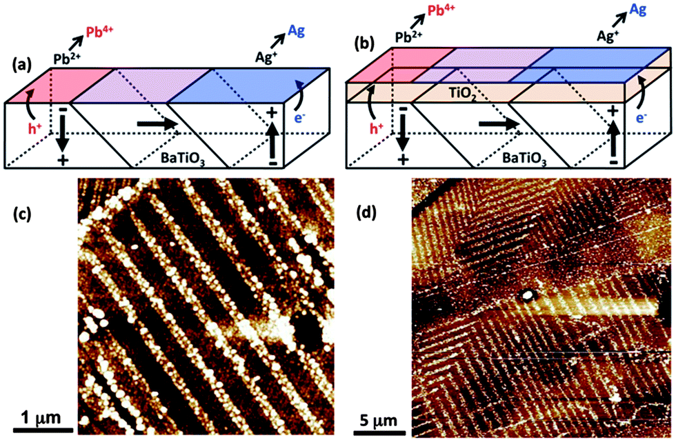 | ||
| Fig. 13 A schematic illustrating that the ferroelectric domains in the substrate promote the redox reactions on both (a) the bare substrate and (b) films surfaces. The AFM images of (c) (100) oriented BaTiO3 substrate and (d) 15 nm thick anatase film supported by (100) oriented BaTiO3 substrate after the photochemical reaction in aqueous silver nitrate solution. (The white contrast in (c) and (d) refers to the solid silver after photochemical reduction). | ||
The application of heterostructured ferroelectric photocatalysts for water splitting, organic dye degradation, and other uses has also been reported. For example, PZT/TiO2 nanostructured heterojunctions show enhanced photocatalytic activity for decomposition of ethylene under visible light illumination.156 Nanostructured composites of BaTiO3/TiO2 are also reported to show an increased antibacterial photocatalytic activity.60 Ag-loaded BaTiO3/TiO2 nanotubes enhanced charge carrier separation and showed higher photocatalytic reacvitity for methylene blue degradation than their components.157 Ferroelectric PbTiO3, when coated with nanostructured TiO2, exhibits improved photocatalytic decomposition of methylene blue under visible light irradiation.50 BiFeO3–TiO2 core–shell nanostructured composites fabricated by the hydrothermal method show a higher photocatalytic activity for the photodegradation of Congo red.158 Currently, more and more attention is focused on the application of polarizable semiconductors to control photochemical reactions, and this approach provides a new strategy for heterostructured photocatalyst design.16
The use of a ferroelectric internal field within a hierarchically structured photocatalyst provides a reasonable method to create more efficient photocatalysts. Micron-sized BaTiO3 cores coated with nanostructured TiO2 showed enhanced photocatalytic activity for hydrogen production compared to the parent phases.58 The internal field arising from the micron-sized ferroelectric core, which is also the primary component for light absorption, separates the photogenerated charge carriers. Electrons and holes are transferred through the interface to the nanostructured TiO2 coating, where the charge carriers participate in the redox reaction with water. For this composite, the structural integrity of the interface is important for charge transfer to the coating. At the same time, the high surface area coating provides a large amount of active sites for the reactions. Note that the design of these two phase hierarchically structured materials can improve the stability of the catalyst by protecting a phase susceptible to corrosion with a more stable coating.59 By manipulating the processing conditions, hierarchically structured catalysts can also be fabricated to improve their physicochemical properties, such as surface area and porosity.159
4.2. Internal fields at phase boundaries
 | ||
| Fig. 14 A schematic illustration of a p–n junction between two semiconductors without an externally applied voltage. | ||
The design of heterostructured photocatalysts consisting of p-type and n-type semiconductor components is one of the most common methods to make composite photocatalysts with improved photocatalytic activity. TiO2, the most common photocatalyst studied, is an n-type semiconductor and is self-doped by oxygen vacancies.89,90,169 The electronic conductivity of titania is determined by a combination of impurities and the composition of the gas in which it was equilibrated at high temperature. While titania is n-type in nearly all conditions, p-type TiO2 was recently prepared by creating titanium vacancies at elevated temperature and pressure, followed by quenching.170 TiO2 has been coupled with different p-type metal oxide photocatalysts, such as Cu2O,171–175 Ag2O,176–178 Co3O4,179 CuAlO2,180 CuBi2O4,181 NiO,182,183 BiOX (X = Cl, Br, I),184–186 FeTiO3,187,188 and ZnMn2O4,172 to design efficient heterostructured photocatalysts. Graphene oxide also can be prepared with p-type electrical conductivity.189 TiO2 was coupled with graphene oxide to form a p–n junction and degraded methylene blue under visible light with wavelengths longer than 510 nm.190 Similar enhancements of the photocatalytic activity of graphene oxide with TiO2 have been reported by others.191–193 Other photochemically active p–n junction combinations, not using TiO2, that have been reported include NiO/ZnO,194 CaFe2O4/Ag3VO4,195 Co3O4/BiVO4,196,197 CuBi2O4/WO3,198 BiOI/(BiO)2CO3,199,200 Cu2O/In2O3,201 Cu2O/BiVO4,41 Cu2O/WO3,202 and Ag3PO4/BiPO4.203 These nanosized particulate photocatalysts with designs similar to photoelectrochemical and photovoltaic cells show enhanced photocatalytic activity for water splitting and organic dye degradation under UV and visible light. Photocatalytic nanodiodes made up of p-type CaFe2O4 interfaced with an n-type perovskite PbBi2Nb1.9W0.1O9 show enhanced photocatalytic activities for oxygen evolution and the degradation of organic pollutants compared to TiO2−xNx under visible light irradiation (λ > 420 nm).204
A p–n junction in the same material also can be achieved through the spatial control of doping. For example, it has been reported that p-type TiO2 has been prepared by doping with metal ions, such as Fe3+,205,206 Cr3+,207,208 Co3+,207,209–212 V,213 and N.214 It has also been reported that p-type TiO2 also can be prepared by co-doping C and W.215 The p–n contact formed at the junction has been confirmed to assist the separation of photogenerated charge carriers and thus increase the photocatalytic activity of the material.209,216,217 It should be noted that though TiO2 can be doped to be a p-type semiconductor, n-type doping is more common. The ability to achieve n-type or p-type doping depends on the positions of the conduction and valance bands.215,218 Lower conduction band energies make it easier to dope a material n-type and higher valence band energies make it easier to dope a material p-type.215 For example, ZnO, ZnS, CdS and CdTe are easily doped n-type, while ZnTe is more easily doped p-type.215,219–223 The p–n junction design has also been applied to the design of photoelectrochemical cells for the enhancement of water splitting. A 20 nm film of p-type hematite doped by Mg was coated with n-type hematite by atomic layer deposition (ALD) and the homojunction showed a 200 mV turn-on voltage shift in the cathodic direction.224 The rapid open circuit voltage decay for the Fe2O3 p–n junction indicates the built-in internal fields help to separate charge in the water splitting conditions. The media is also important for adjusting the electrical conductivity of semiconductors. The dominant charge carrier type can be affected by the pH of the electrolyte and can be tunable from n-type to p-type when prepared in acid or alkaline solutions.225–227 As shown in Fig. 15, a Cu2O p–n junction film was prepared by a two-step electrodeposition in acid and subsequent alkaline or neutral solution. The final result shows that the p-Cu2O(pH = 9)/n-Cu2O(pH = 4.9) has the largest interfacial electric field and high charge separation efficiency.228
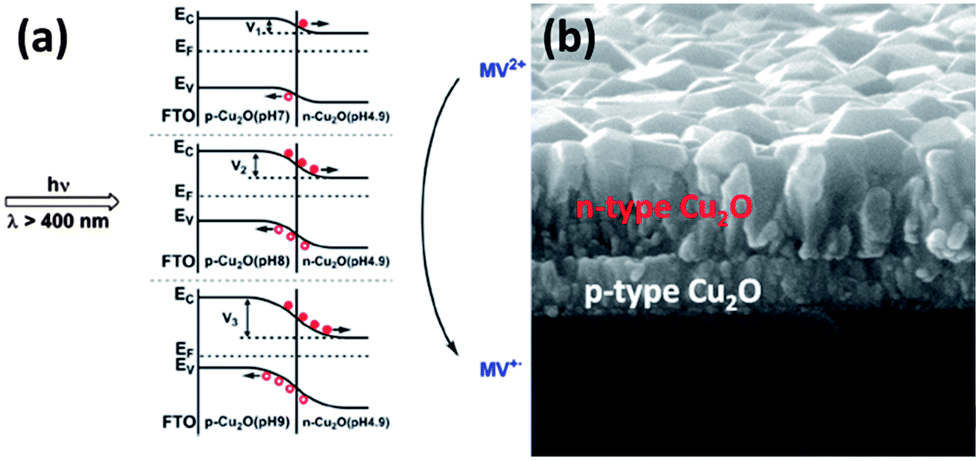 | ||
| Fig. 15 Energy level diagram and charge transfer process for Cu2O p–n homojunction prepared by electrodeposition with different pH conditions for methyl viologen (MV2+) photo-reduction to the reduced form (MV+), and thus with different magnitude of interfacial electric field. (b) SEM cross section image of Cu2O p–n homojunction film (reproduced from ref. 228). | ||
Note that a stable interface with a small structural discontinuity between the components at the junctions is important for photogenerated charge carrier transfer. Charge transfer between semiconductor interfaces is finished within picoseconds,40,229 and this fast transfer rate requires the interface to provide the smallest penetration barrier. The fabrication of a high quality interfaces in heterostructured catalysts is attracting more and more attention.229–231 Previous results showed that micron scale ATiO3 (A = Pb, Fe) coated with nanostructured TiO2 had a higher reactivity for photodecomposition of methylene blue than AFeO3 (A = Bi, La, Y)/TiO2 processed at the same conditions.232 The photocatalytic activity enhancement of titanate/TiO2 material over ferrite/TiO2 material is attributed to the continuity of bonding at the interface between the titanate core and shell.
Hierarchically structured photocatalysts with p–n junctions have also been designed and used for photochemical reactions. TiO2 nanoparticles were deposited on the surface of hierarchical flowerlike NiO and the composites show enhanced photodegradation for p-chlorophenol compared to the components prepared using the same conditions.233 The enhanced photocatalytic activity is attributed to the p–n junction formation, which provides an internal field for charge separation, and the hierarchical structure, which decreases the aggregation of TiO2 and promotes the transport of reactants and products. Double shell Bi2O3/Bi2WO6 hollow spheres show higher photocatalytic activity than the component phases.234 In addition to the formation of a p–n junction, the increase of light harvesting in the hierarchical structure leads to an increase of the photocatalytic reactivity. Other hierarchical structures with nanobelt,235 nanorod,236 and nanobrush237 morphologies are widely reported to form p–n junctions and promote increased the photocatalytic reactivity.
Polar surface terminations, even if they only occur locally, can create fields that will influence the photochemical activity of materials. For example, the photochemical reduction of Ag+ and oxidation of Pb2+ on the surface of SrTiO3 is anisotropic.43 The internal field created by a polar surface termination can promote the separation of photogenerated charge carriers and spatially selective oxidation and reduction. The two AFM images in Fig. 16(a) and (b) are the topography of a (111)-oriented SrTiO3 single crystal before and after photochemical reduction of Ag. The result shows that silver is only reduced on specific terraces, which means the photochemical reduction is spatially separated. This was shown to be correlated to the terminations of the different terraces. The ideal bulk-truncated (111) surface of SrTiO3 can only be terminated by a negatively charged SrO34− layer or by a positively charged Ti4+ layer, as shown in Fig. 16(c) and (d). These charged surfaces promote spatially selective oxidation and reduction reactions, similar to those that occur on the different domains of a ferroelectric. The same experiment was performed on (100) surfaces, which can only be terminated by non-polar SrO or TiO2 surfaces. In this case, the silver was reduced uniformly on all terraces. It has also been reported that non-ferroelectric SrTiO3 can show ferroelectricity on its surface or under strained/unstrained conditions.239–242 SrTiO3/TiO2 is reported to show higher photocatalytic activity for organic dye degradation243 and hydrogen production than its components.59,244,245 Hierarchically structured SrTiO3/TiO2 nanofibers have also been used for photocatalytic water splitting.246
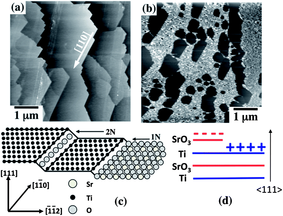 | ||
| Fig. 16 The influence of dipolar field created by polar surface termination on the photochemical reactivity of SrTiO3. Topographic AFM images of the (111) surface of a SrTiO3 single crystal. (a) Before the reactions. (b) The same surface after illumination in an aqueous AgNO3 solution. The white contrast corresponds to silver. The ranges of the vertical black-to-white contrast in (a) and (b) are 60 nm and 200 nm respectively. Schematic drawing of the possible SrTiO3(111) surface terminations. The left hand terrace has a Ti4+ termination. Traversing an even-N step does not change the chemical termination while traversing an odd-N step changes the chemical termination to SrO34− (right terrace). Note that the step edges are {100} type. Layer spacing (N) = √3a/6 = 1.12 Å.43 | ||
For example, four different polymorphs of TiO2 have been reported, namely, anatase (tetragonal, space group I41/amd), rutile (tetragonal, space group P42/mnm), brookite (orthorhombic, space group Pbca), and TiO2 (B) (monoclinic, space group C2/m). While only one of the phases is in equilibrium at a specific temperature and pressure, all four can be metastable in ambient conditions.74,249–253 Note that when heating is used to transform one phase to another, this also changes the particle size, crystallinity, porosity, and the surface OH− concentration, and all of these factors can also affect the photochemical activity.59,79,80,254 The photocatalytic activity of those four phases has been compared in a number of experiments.255–258 Anatase is generally considered to be more photoactive than rutile, even though it has a relatively larger bandgap.75,78,249,259 However, it has also been shown that if a sensitizing dye is used to inhibit recombination, the photoactivity of rutile is similar to anatase.77
It has been shown that combining titania polymorphs can lead to enhanced photocatalytic activity. One of the representative examples for this is the commercial product Degussa P25. P25 is composed of anatase and rutile and it has shown to be more photocatalytically activity than its pure phase components.78,260,261 Nanosized patches of anatase (smaller than 20 nm) are supported on the surface of rutile with a larger particle size (25–30 nm) in P25.262 Hurum et al. investigated P25 with EPR spectroscopy and attributed the enhanced photocatalytic activity to the stabilization of charge separation by electron transfer between anatase and rutile.78 The different conduction and valance band positions lead to the formation of a potential difference between the component phases and assist the migration of charge carriers between phases. In addition, the different band gap energy and particle size also can extend the range of light absorption to the visible region and more electrons can transfer between the interface of anatase and rutile. Other mixtures of TiO2 phases also show improved photocatalytic activity for solar energy conversion. TiO2 (B) in different morphologies, such as nanofibers, coupled with anatase, has been reported to show high photocatalytic activity.47,249,263,264 Yang et al. fabricated TiO2 (B) nanofibers coated with anatase shells and the heterostructured materials were used for the degradation of the organic pollutant sulforhodamine B.249 The TiO2 (B)/anatase composite was more photocatalytically reactive than its components and had a reactivity similar to Degussa P25, as shown in Fig. 17. TiO2 (B) has a narrower band gap and lower conduction band position than anatase. The difference in band gap positions induces a potential difference, and part of electrons and holes from the anatase will migrate to the TiO2 (B). Because of the faster transfer rate of hole transfer (1–4 ps) to TiO2 (B) than electrons (>40–160 ps), the recombination rate of those charge carriers can be decreased for the heterostructured materials. Meanwhile, the similarity in crystallographic registry between anatase and TiO2 (B) can increase the structural stability and the operation time of the photocatalyst. Anatase coated on the surface of rutile, a configuration similar to P25, produces four times more photocatalytic H2 than pure rutile TiO2.265 Anatase/rutile structures with controlled microstructure and thickness were used for dye decoloration and CH3CHO oxidation.266,267 The controlled combinations of those two TiO2 polymorph junctions affected the formation of Schottky potential barriers and the charge separation distances. The enhancement of photocatalytic activity in the structures compared to their components was attributed to the transfer of photogenerated charge carriers between the different phases, which decreases recombination. Brookite and anatase composites were also found to have high photocatalytic activity, for example, for the oxidation of CH3CHO, and this was also attributed to electron transfer between the phases.268,269 Anatase/brookite nanoparticle mixtures also showed higher photocatalytic hydrogen production from methanol–water solutions than anatase alone, even though the surface area was smaller.270 The combination of brookite and rutile was also confirmed to be highly effective for RhB photo-decolorization and its reactivity was about six times of that of P25.271 A triple phase mixture of anatase, rutile and brookite also showed higher photocatalytic activity for 4-nitrophenol degradation than the single phases.272
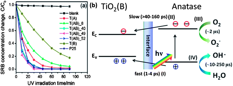 | ||
| Fig. 17 (a) Photocatalytic degradation of SRB with various TiO2 photocatalysts (T(A) stands for anatase TiO2, T(B) for TiO2 (B) and T(AB) for the composite of anatase and TiO2 (B)). (b) Schematic of electron–hole separation between TiO2 (B) and anatase in the composite nanofibers under UV illumination (reproduced from ref. 249). | ||
A similar polymorphic junction was also observed for Ga2O3. Ga2O3, which is n-type, has five polymorph phases,273 of which the α-Ga2O3 (rhombohedral) and β-Ga2O3 (monoclinic) phases are considered as more photocatalytically active for hydrogen production by water splitting, organic dye degradation, nonoxidative coupling of CH4, and the reduction of CO2 than the other phases.274–282 β-Ga2O3 is reported to show the highest photocatalytic activity because of the long lifetime of photogenerated charge carriers in this phase, which are separated by the local internal fields induced from the coexistence of distorted tetrahedral and octahedral units.280 Wang et al. has successfully prepared α-Ga2O3 and β-Ga2O3 junctions through the phase transformation from α-Ga2O3 at elevated temperature.247 The β phase is more thermally stable than the α-phase and its fraction of the total increased with the annealing temperature. Therefore, the fraction of α-Ga2O3 and β-Ga2O3 can be tuned by adjusting the processing temperature from 863–903 K. The α–β phase junction was prepared with well-matched lattice fringes, as shown in Fig. 18, and showed much higher photocatalytic activity for water splitting under UV-light irradiation than the pure α or β phases. The enhanced photocatalytic activity is attributed to the junction formed at the interface between two phases. The difference in the conduction band position leads to internal fields that facilitate the transfer of electrons and holes between the phases and decreases the recombination of photogenerated charge carriers.
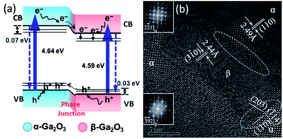 | ||
| Fig. 18 (a) Illustration of α–β phase junction for charge separation and enhanced photocatalytic activity and (b) HRTEM image of the interface between α and β-Ga2O3 phase. (The figure is reproduced from ref. 247). | ||
Considering that many semiconductors are polymorphic, polymorph junctions might provide a mechanism for the efficient separation of charge carriers and, therefore, a path for increasing the efficiency of the photocatalysts. The fact that the composition on both sides of the interface is the same provides continuity of the bonding across the polymorph boundary, which may facilitate the charge transfer across the interface. The polymorph junction approach may provide a new strategy for the efficient photocatalysts design, as well as other solar energy conversion devices, such as photovoltaic and photoelectrochemical devices.
5 Prospective and summary
In the current review, we focused on the use of electric fields within semiconductors to separate photogenerated charge carriers and modify photocatalytic properties. Four internal field sources have been described: ferroelectric polarization, polar surfaces, p–n junctions and polymorph junctions, as illustrated schematically in Fig. 19. The presence of the internal field changes the band bending at interfaces and provides a driving force for the separation of photogenerated electrons and holes. The distribution and direction of internal fields can be controlled so that redox reactions will occur in different places, which also decrease the back reaction of the intermediates. The manipulation of internal fields within photochemically active materials is a promising strategy for the improvement of photocatalysts.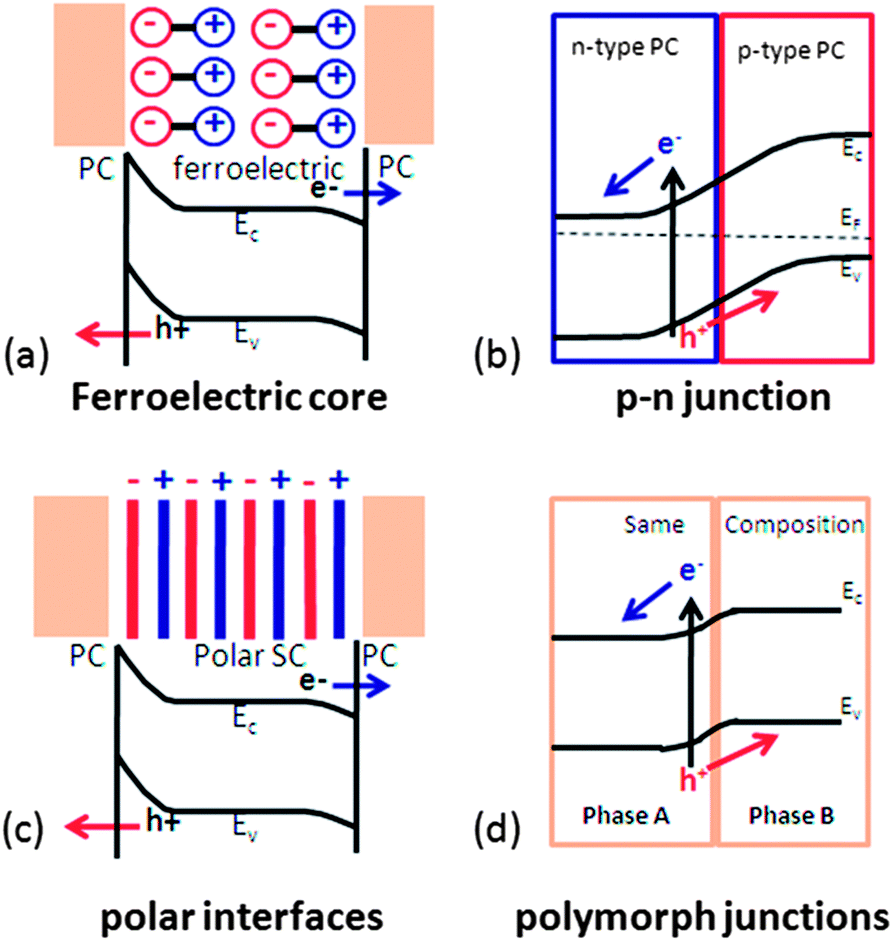 | ||
| Fig. 19 The internal field enhanced photogenerated charge carrier separation: (a) ferroelectric polarization; (b) p–n junctions; (c) polar surfaces; and (d) polymorph junctions. (PC: photocatalytic active materials; SC: semiconductor). | ||
One method for simultaneously controlling interface fields and the density of active sites is to create hierarchically structured composite materials. For example, visible light responsive materials can be coupled with materials that have internal fields and extend the performance of heterostructured photocatalysts to the visible light range. Other methods, such as doping and dye sensitization, can be combined with internal fields to design efficient visible light photocatalysts. For heterostructured photocatalysts, interface quality is important. A low defect density and chemically strong bonds across interfaces with large contact areas is preferred for electron and hole transfer. Therefore, processing techniques to engineer the interface integrity are needed. It must also be recognized that internal fields are size dependent. For example, ferroelectric polarization has been confirmed to decrease greatly below crystal sizes of about 100 nm. On the other hand, the relationship between surface area and catalytic activity means smaller sizes are preferred for photochemical processes. Therefore, the particle size for photocatalytic materials must be selected to simultaneously optimize the positive effects of internal fields and surface area. Considering those factors, it is concluded that the manipulation of internal fields and hierarchical structures may lead to improved catalysts for water splitting and other solar energy conversion processes.
Acknowledgements
This work was supported by National Science Foundation grant DMR 1206656 and the PA DCED.Notes and references
- A. Fujishima, X. Zhang and D. A. Tryk, Int. J. Hydrogen Energy, 2007, 32, 2664–2672 CrossRef CAS.
- A. Kudo, Int. J. Hydrogen Energy, 2006, 31, 197–202 CrossRef CAS.
- D. Y. C. Leung, X. L. Fu, C. F. Wang, M. Ni, M. K. H. Leung, X. X. Wang and X. Z. Fu, ChemSusChem, 2010, 3, 681–694 CrossRef CAS PubMed.
- C. Chen, W. Ma and J. Zhao, Chem. Soc. Rev., 2010, 39, 4206–4219 RSC.
- A. J. Esswein and D. G. Nocera, Chem. Rev., 2007, 107, 4022–4047 CrossRef CAS PubMed.
- A. Kudo and Y. Miseki, Chem. Soc. Rev., 2009, 38, 253–278 RSC.
- K. Maeda, K. Teramura, D. L. Lu, T. Takata, N. Saito, Y. Inoue and K. Domen, Nature, 2006, 440, 295–295 CrossRef CAS PubMed.
- K. Maeda, K. Teramura, D. Lu, N. Saito, Y. Inoue and K. Domen, Angew. Chem., Int. Ed., 2006, 45, 7806–7809 CrossRef CAS PubMed.
- S. Y. Reece, J. A. Hamel, K. Sung, T. D. Jarvi, A. J. Esswein, J. J. H. Pijpers and D. G. Nocera, Science, 2011, 334, 645–648 CrossRef CAS PubMed.
- H. Kato, K. Asakura and A. Kudo, J. Am. Chem. Soc., 2003, 125, 3082–3089 CrossRef CAS PubMed.
- J. F. Reber and K. Meier, J. Phys. Chem., 1984, 88, 5903–5913 CrossRef CAS.
- X. Chen, L. Liu, P. Y. Yu and S. S. Mao, Science, 2011, 331, 746–750 CrossRef CAS PubMed.
- R. Asahi, T. Morikawa, T. Ohwaki, K. Aoki and Y. Taga, Science, 2001, 293, 269–271 CrossRef CAS PubMed.
- Z. G. Zou, J. H. Ye, K. Sayama and H. Arakawa, Nature, 2001, 414, 625–627 CrossRef CAS PubMed.
- Y. Inoue, Energy Environ. Sci., 2009, 2, 364–386 CAS.
- D. Tiwari and S. Dunn, J. Mater. Sci., 2009, 44, 5063–5079 CrossRef CAS.
- Z. Zhang and J. T. Yates, Chem. Rev., 2012, 112, 5520–5551 CrossRef CAS PubMed.
- F. E. Osterloh, Chem. Mater., 2008, 20, 35–54 CrossRef CAS.
- F. E. Osterloh, Chem. Soc. Rev., 2013, 42, 2294–2320 RSC.
- X. Chen, S. Shen, L. Guo and S. S. Mao, Chem. Rev., 2010, 110, 6503–6570 CrossRef CAS PubMed.
- X. Chen, C. Li, M. Gratzel, R. Kostecki and S. S. Mao, Chem. Soc. Rev., 2012, 41, 7909–7937 RSC.
- G. N. Schrauzer and T. D. Guth, J. Am. Chem. Soc., 1977, 99, 7189–7193 CrossRef CAS.
- B. Kraeutler and A. J. Bard, J. Am. Chem. Soc., 1978, 100, 4317–4318 CrossRef CAS.
- K. Masao and O. Ichiro, Photocatalysis Science and Technology, Springer, 2002 Search PubMed.
- D. A. Tryk, A. Fujishima and K. Honda, Electrochim. Acta, 2000, 45, 2363–2376 CrossRef CAS.
- K. Domen, in Surface Photochemistry, ed. M. Anpo, J. Wiley & Sons, Chichester, 1996, pp. 1–18 Search PubMed.
- W. J. Albery and N. B. Philip, J. Electrochem. Soc., 1984, 131, 315–325 CrossRef CAS.
- M. D. Hernandez-Alonso, F. Fresno, S. Suarez and J. M. Coronado, Energy Environ. Sci., 2009, 2, 1231–1257 CAS.
- K. Maeda and K. Domen, J. Phys. Chem. Lett., 2010, 1, 2655–2661 CrossRef CAS.
- M. C. A. G. Rufino, M. Navarro Yerga, F. del Valle, J. A. Villoria de la Mano and J. L. G. Fierro, ChemSusChem, 2009, 2, 471–485 CrossRef PubMed.
- U. A. Joshi, A. Palasyuk, D. Arney and P. A. Maggard, J. Phys. Chem. Lett., 2010, 1, 2719–2726 CrossRef CAS.
- T. Tachikawa, M. Fujitsuka and T. Majima, J. Phys. Chem. C, 2007, 111, 5259–5275 CAS.
- K. Rajeshwar, J. Appl. Electrochem., 2007, 37, 765–787 CrossRef CAS.
- K. Maeda, K. Teramura, D. L. Lu, T. Takata, N. Saito, Y. Inoue and K. Domen, J. Phys. Chem. B, 2006, 110, 13753–13758 CrossRef CAS PubMed.
- K. Maeda, T. Takata, M. Hara, N. Saito, Y. Inoue, H. Kobayashi and K. Domen, J. Am. Chem. Soc., 2005, 127, 8286–8287 CrossRef CAS PubMed.
- S. R. Morrison, Electrochemistry at semiconductor and oxidized metal electrodes, Plenum Press, New York, 1980 Search PubMed.
- A. L. Linsebigler, G. Lu and J. T. Yates, Chem. Rev., 1995, 95, 735–758 CrossRef CAS.
- A. J. Nozik and R. Memming, J. Phys. Chem., 1996, 100, 13061–13078 CrossRef CAS.
- J. Yang, D. Wang, H. Han and C. Li, Acc. Chem. Res., 2013, 46, 1900–1909 CrossRef CAS PubMed.
- P. V. Kamat, J. Phys. Chem. Lett., 2012, 3, 663–672 CrossRef CAS PubMed.
- W. Wang, X. Huang, S. Wu, Y. Zhou, L. Wang, H. Shi, Y. Liang and B. Zou, Appl. Catal., B, 2013, 134–135, 293–301 CrossRef CAS.
- X. Lin, J. Xing, W. Wang, Z. Shan, F. Xu and F. Huang, J. Phys. Chem. C, 2007, 111, 18288–18293 CAS.
- J. L. Giocondi and G. S. Rohrer, J. Am. Ceram. Soc., 2003, 86, 1182–1189 CrossRef CAS.
- Y. Matsumoto, T. Ohsawa, R. Takahashi and H. Koinuma, Thin Solid Films, 2005, 486, 11–14 CrossRef CAS.
- N. Kislov, J. Lahiri, H. Verma, D. Y. Goswami, E. Stefanakos and M. Batzill, Langmuir, 2009, 25, 3310–3315 CrossRef CAS PubMed.
- G. Liu, J. C. Yu, G. Q. Lu and H.-M. Cheng, Chem. Commun., 2011, 47, 6763–6783 RSC.
- W. Li, C. Liu, Y. Zhou, Y. Bai, X. Feng, Z. Yang, L. Lu, X. Lu and K.-Y. Chan, J. Phys. Chem. C, 2008, 112, 20539–20545 CAS.
- G. Tian, H. Fu, L. Jing, B. Xin and K. Pan, J. Phys. Chem. C, 2008, 112, 3083–3089 CAS.
- J. L. Giocondi and G. S. Rohrer, Top. Catal., 2008, 49, 18–23 CrossRef CAS.
- L. Li, Y. Zhang, A. M. Schultz, X. Liu, P. A. Salvador and G. S. Rohrer, Catal. Sci. Technol., 2012, 2, 1945–1952 CAS.
- Y. Gou, D. Chen and Z. Su, Appl. Catal., A, 2004, 261, 15–18 CrossRef CAS.
- R. Qiu, D. Zhang, Y. Mo, L. Song, E. Brewer, X. Huang and Y. Xiong, J. Hazard. Mater., 2008, 156, 80–85 CrossRef CAS PubMed.
- H.-C. Liang and X.-Z. Li, Appl. Catal., B, 2009, 86, 8–17 CrossRef CAS.
- K. Hashimoto, H. Irie and A. Fujishima, Jpn. J. Appl. Phys., 2005, 44, 8269–8285 CrossRef CAS.
- M. Kitano and M. Hara, J. Mater. Chem., 2010, 20, 627–641 RSC.
- J. F. Reber and M. Rusek, J. Phys. Chem., 1986, 90, 824–834 CrossRef CAS.
- N. Buhler, K. Meier and J. F. Reber, J. Phys. Chem., 1984, 88, 3261–3268 CrossRef.
- L. Li, G. S. Rohrer and P. A. Salvador, J. Am. Ceram. Soc., 2012, 95, 1414–1420 CrossRef CAS.
- L. Li, X. Liu, Y. Zhang, P. A. Salvador and G. S. Rohrer, Int. J. Hydrogen Energy, 2013, 38, 6948–6959 CrossRef CAS.
- S. E. Stanca, R. Muller, M. Urban, A. Csaki, F. Froehlich, C. Krafft, J. Popp and W. Fritzsche, Catal. Sci. Technol., 2012, 2, 1472–1479 CAS.
- Z. Zhang, C.-C. Wang, R. Zakaria and J. Y. Ying, J. Phys. Chem. B, 1998, 102, 10871–10878 CrossRef CAS.
- D. Beydoun, R. Amal, G. Low and S. McEvoy, J. Nanopart. Res., 1999, 1, 439–458 CrossRef CAS.
- A. Bhardwaj, N. V. Burbure, A. Gamalski and G. S. Rohrer, Chem. Mater., 2010, 22, 3527–3534 CrossRef CAS.
- W. J. Albery and P. N. Bartlett, J. Electrochem. Soc., 1984, 131, 315–325 CrossRef CAS.
- U. Banin, Y. W. Cao, D. Katz and O. Millo, Nature, 1999, 400, 542–544 CrossRef CAS.
- X. G. Peng, L. Manna, W. D. Yang, J. Wickham, E. Scher, A. Kadavanich and A. P. Alivisatos, Nature, 2000, 404, 59–61 CrossRef CAS PubMed.
- Y. Wang and N. Herron, J. Phys. Chem., 1991, 95, 525–532 CrossRef CAS.
- J. Pan, G. Liu, G. Q. Lu and H.-M. Cheng, Angew. Chem., Int. Ed., 2011, 50, 2133–2137 CrossRef CAS PubMed.
- G. Liu, C. Sun, H. G. Yang, S. C. Smith, L. Wang, G. Q. M. Lu and H.-M. Cheng, Chem. Commun., 2010, 46, 755–757 RSC.
- J. Giocondi, P. Salvador and G. Rohrer, Top. Catal., 2007, 44, 529–533 CrossRef CAS.
- R. Li, F. Zhang, D. Wang, J. Yang, M. Li, J. Zhu, X. Zhou, H. Han and C. Li, Nat. Commun., 2013, 4, 1432 CrossRef PubMed.
- W. E. Farneth, R. S. McLean, J. D. Bolt, E. Dokou and M. A. Barteau, Langmuir, 1999, 15, 8569–8573 CrossRef CAS.
- P. A. Morris Hotsenpiller, J. D. Bolt, W. E. Farneth, J. B. Lowekamp and G. S. Rohrer, J. Phys. Chem. B, 1998, 102, 3216–3226 CrossRef.
- H. Z. Zhang and J. F. Banfield, J. Phys. Chem. B, 2000, 104, 3481–3487 CrossRef CAS.
- A. Sclafani and J. M. Herrmann, J. Phys. Chem., 1996, 100, 13655–13661 CrossRef CAS.
- L. Kavan, M. Grätzel, S. E. Gilbert, C. Klemenz and H. J. Scheel, J. Am. Chem. Soc., 1996, 118, 6716–6723 CrossRef CAS.
- N. G. Park, J. van de Lagemaat and A. J. Frank, J. Phys. Chem. B, 2000, 104, 8989–8994 CrossRef CAS.
- D. C. Hurum, A. G. Agrios, K. A. Gray, T. Rajh and M. C. Thurnauer, J. Phys. Chem. B, 2003, 107, 4545–4549 CrossRef CAS.
- C. K. Chan, J. F. Porter, Y. G. Li, W. Guo and C. M. Chan, J. Am. Ceram. Soc., 1999, 82, 566–572 CrossRef CAS.
- Q. H. Zhang, L. Gao and J. K. Guo, Appl. Catal., B, 2000, 26, 207–215 CrossRef CAS.
- L. Gao and Q. H. Zhang, Scr. Mater., 2001, 44, 1195–1198 CrossRef CAS.
- R. M. Noyes, J. Am. Chem. Soc., 1962, 84, 513–522 CrossRef CAS.
- S. Trasatti, J. Electroanal. Chem., 1974, 52, 313–329 CrossRef CAS.
- W. N. Hansen and D. M. Kolb, J. Electroanal. Chem., 1979, 100, 493–500 CrossRef CAS.
- M. A. Butler and D. S. Ginley, J. Electrochem. Soc., 1978, 125, 228–232 CrossRef CAS.
- A. J. Nozik, Annu. Rev. Phys. Chem., 1978, 29, 189–222 CrossRef CAS.
- H. Luth, Solid Surfaces, Interfaces and Thin Films, Springer Berlin Heidelberg, New York, 2010 Search PubMed.
- M. Gratzel, Nature, 2001, 414, 338–344 CrossRef CAS PubMed.
- T. Bak, J. Nowotny, M. Rekas and C. C. Sorrell, J. Phys. Chem. Solids, 2003, 64, 1043–1056 CrossRef CAS.
- M. K. Nowotny, T. Bak and J. Nowotny, J. Phys. Chem. B, 2006, 110, 16270–16282 CrossRef CAS PubMed.
- J. Liqiang, S. Xiaojun, S. Jing, C. Weimin, X. Zili, D. Yaoguo and F. Honggang, Sol. Energy Mater. Sol. Cells, 2003, 79, 133–151 CrossRef.
- W. Monch, Electronic Properties of Semiconductor Interfaces, Springer-Verlag, New York, 2004 Search PubMed.
- A. Fujishima, T. N. Rao and D. A. Tryk, J. Photochem. Photobiol., C, 2000, 1, 1–21 CrossRef CAS.
- A. Beer, Phys. Chem., 1852, 86, 78 Search PubMed.
- H. A. Liebhafsky and H. G. Pfeiffer, J. Chem. Educ., 1953, 30, 450 CrossRef CAS.
- H. Tang, F. Levy, H. Berger and P. E. Schmid, Phys. Rev. B: Condens. Matter Mater. Phys., 1995, 52, 7771–7774 CrossRef CAS.
- Y. R. Park and K. J. Kim, Thin Solid Films, 2005, 484, 34–38 CrossRef CAS.
- S. P. Albu, A. Ghicov, J. M. Macak, R. Hahn and P. Schmuki, Nano Lett., 2007, 7, 1286–1289 CrossRef CAS PubMed.
- N. V. Burbure, P. A. Salvador and G. S. Rohrer, J. Am. Ceram. Soc., 2006, 89, 2943–2945 CAS.
- A. J. Nozik, Appl. Phys. Lett., 1977, 30, 567–569 CrossRef CAS.
- J. L. Giocondi and G. S. Rohrer, J. Phys. Chem. B, 2001, 105, 8275–8277 CrossRef CAS.
- J. L. Giocondi and G. S. Rohrer, Chem. Mater., 2001, 13, 241–242 CrossRef CAS.
- K. M. Rabe, C. H. Ahn and J.-M. Triscone, Physics of Ferroelectrics: A Modern Perspective, Springer, 2007 Search PubMed.
- M. E. Lines and A. M. Glass, Principles and applications of ferroelectrics and related materials, Clarendon Press, Oxford, 1977 Search PubMed.
- D. Damjanovic, Rep. Prog. Phys., 1998, 61, 1267–1324 CrossRef CAS.
- C. H. Ahn, K. M. Rabe and J. M. Triscone, Science, 2004, 303, 488–491 CrossRef CAS PubMed.
- M. E. Lines and A. M. Glass, Principles and Applications of Ferroelectrics and Related Materials, Clarendon Press, Oxford, 2001 Search PubMed.
- N. Braithwaite and G. Weaver, Materials in action series – electronic materials inside electronic devices, Alden Press (London & Northampton) Ltd, London, 1998 Search PubMed.
- T. Mitsui, I. Tatsuzaki and E. Nakamura, An Introduction to the Physics of Ferroelectris, Gordon and Breach Science Publishers, 1976 Search PubMed.
- E. K. Akdogan, C. J. Rawn, W. D. Porter, E. A. Payzant and A. Safari, J. Appl. Phys., 2005, 97, 084305 CrossRef.
- M. Yashima, T. Hoshina, D. Ishimura, S. Kobayashi, W. Nakamura, T. Tsurumi and S. Wada, J. Appl. Phys., 2005, 98, 014313 CrossRef.
- K. Uchino, E. Sadanaga and T. Hirose, J. Am. Ceram. Soc., 1989, 72, 1555–1558 CrossRef CAS.
- X. P. Li and W. H. Shih, J. Am. Ceram. Soc., 1997, 80, 2844–2852 CrossRef CAS.
- Naumov II, L. Bellaiche and H. X. Fu, Nature, 2004, 432, 737–740 CrossRef PubMed.
- M. J. Polking, M.-G. Han, A. Yourdkhani, V. Petkov, C. F. Kisielowski, V. V. Volkov, Y. Zhu, G. Caruntu, A. Paul Alivisatos and R. Ramesh, Nat. Mater., 2012, 11, 700–709 CrossRef CAS PubMed.
- L. Zhang, W. L. Zhong, C. L. Wang, Y. P. Peng and Y. G. Wang, Eur. Phys. J. B, 1999, 11, 565–573 CrossRef CAS.
- A. M. Glass, D. von der Linde and T. J. Negran, Appl. Phys. Lett., 1974, 25, 233–235 CrossRef CAS.
- O. Ambacher, J. Smart, J. R. Shealy, N. G. Weimann, K. Chu, M. Murphy, W. J. Schaff, L. F. Eastman, R. Dimitrov, L. Wittmer, M. Stutzmann, W. Rieger and J. Hilsenbeck, J. Appl. Phys., 1999, 85, 3222–3233 CrossRef CAS.
- R. C. Casella and S. P. Keller, Phys. Rev., 1959, 116, 1469–1473 CrossRef CAS.
- M. Cardona, Phys. Rev., 1965, 140, A651–A655 CrossRef.
- H. H. Kung, H. S. Jarrett, A. W. Sleight and A. Ferretti, J. Appl. Phys., 1977, 48, 2463–2469 CrossRef CAS.
- C. N. Berglund and H. J. Braun, Phys. Rev., 1967, 164, 790 CrossRef.
- A. J. Bard and L. R. Faulkner, Electrochemical methods: fundamentals and applications, John Wiley & Sons, Inc., New York, 2001 Search PubMed.
- Y. Inoue, K. Sato, K. Sato and H. Miyama, J. Phys. Chem., 1986, 90, 2809–2810 CrossRef CAS.
- P. M. Jones, D. E. Gallardo and S. Dunn, Chem. Mater., 2008, 20, 5901–5906 CrossRef CAS.
- S. Dunn, P. M. Jones and D. E. Gallardo, J. Am. Chem. Soc., 2007, 129, 8724–8728 CrossRef CAS PubMed.
- P. M. Jones and S. Dunn, Nanotechnology, 2007, 18, 185702 CrossRef.
- S. Dunn, S. Sharp and S. Burgess, Nanotechnology, 2009, 20, 115604 CrossRef CAS PubMed.
- P. M. Jones and S. Dunn, J. Phys. D: Appl. Phys., 2009, 42, 065408 CrossRef.
- S. V. Kalinin, D. A. Bonnell, T. Alvarez, X. Lei, Z. Hu, J. H. Ferris, Q. Zhang and S. Dunn, Nano Lett., 2002, 2, 589–593 CrossRef CAS.
- J. Chen, H. Lu, H.-J. Liu, Y.-H. Chu, S. Dunn, A. Gruverman and N. Valanoor, Appl. Phys. Lett., 2013, 102, 182904 CrossRef.
- X. Liu, K. Kitamura, K. Terabe, H. Hatano and N. Ohashi, Appl. Phys. Lett., 2007, 91, 044101 CrossRef.
- M. Stock and S. Dunn, J. Phys. Chem. C, 2012, 116, 20854–20859 CAS.
- A. M. Schultz, Y. Zhang, P. A. Salvador and G. S. Rohrer, ACS Appl. Mater. Interfaces, 2012, 3, 1562–1567 Search PubMed.
- Z. Liu, Y. Qi and C. Lu, J. Mater. Sci.: Mater. Electron., 2010, 21, 380–384 CrossRef CAS.
- F. Gao, X. Y. Chen, K. B. Yin, S. Dong, Z. F. Ren, F. Yuan, T. Yu, Z. Zou and J. M. Liu, Adv. Mater., 2007, 19, 2889–2892 CrossRef CAS.
- X. Lu, J. Xie, Y. Song and J. Lin, J. Mater. Sci., 2007, 42, 6824–6827 CrossRef CAS.
- C. M. Cho, J. H. Noh, I. S. Cho, J. S. An, K. S. Hong and J. Y. Kim, J. Am. Ceram. Soc., 2008, 91, 3753–3755 CrossRef CAS.
- S. Li, Y.-H. Lin, B.-P. Zhang, C.-W. Nan and Y. Wang, J. Appl. Phys., 2009, 105, 056105 CrossRef.
- S. Li, Y.-H. Lin, B.-P. Zhang, Y. Wang and C.-W. Nan, J. Phys. Chem. C, 2010, 114, 2903–2908 CAS.
- H. van Damme and W. K. Hall, J. Catal., 1981, 69, 371–383 CrossRef CAS.
- K. Domen, A. Kudo, A. Shinozaki, A. Tanaka, K. Maruya and T. Onishi, J. Chem. Soc., Chem. Commun., 1986, 356–357 RSC.
- Q. Wu, D. Li, L. Wu, J. Wang, X. Fu and X. Wang, J. Mater. Chem., 2006, 16, 1116–1117 RSC.
- Y. Inoue, I. Yoshioka and K. Sato, J. Phys. Chem., 1984, 88, 1148–1151 CrossRef CAS.
- A. Kudo, A. Tanaka, K. Domen, K. Maruya, K. Aika and T. Onishi, J. Catal., 1988, 111, 67–76 CrossRef CAS.
- Y. Inoue, K. Sato and K. Sato, J. Chem. Soc., Faraday Trans. 1, 1989, 85, 1765–1774 RSC.
- T. Takata, Y. Furumi, K. Shinohara, A. Tanaka, M. Hara, J. N. Kondo and K. Domen, Chem. Mater., 1997, 9, 1063–1064 CrossRef CAS.
- S. Ikeda, M. Hara, J. N. Kondo, K. Domen, H. Takahashi, T. Okubo and M. Kakihana, Chem. Mater., 1998, 10, 72–77 CrossRef CAS.
- A. Kudo, H. Kato and S. Nakagawa, J. Phys. Chem. B, 1999, 104, 571–575 CrossRef.
- H. G. Kim, O. S. Becker, J. S. Jang, S. M. Ji, P. H. Borse and J. S. Lee, J. Solid State Chem., 2006, 179, 1214–1218 CrossRef CAS.
- Y. Inoue, M. Okamura and K. Sato, J. Phys. Chem., 1985, 89, 5184–5187 CrossRef CAS.
- Y. Inoue, K. Sato and S. Suzuki, J. Phys. Chem., 1985, 89, 2827–2831 CrossRef CAS.
- N. V. Burbure, P. A. Salvador and G. S. Rohrer, Chem. Mater., 2010, 22, 5831–5837 CrossRef CAS.
- N. V. Burbure, P. A. Salvador and G. S. Rohrer, Chem. Mater., 2010, 22, 5823–5830 CrossRef CAS.
- Y. Zhang, A. M. Schultz, P. A. Salvador and G. S. Rohrer, J. Mater. Chem., 2011, 21, 4168–4174 RSC.
- H. J. Huang, D. Z. Li, Q. Lin, Y. Shao, W. Chen, Y. Hu, Y. B. Chen and X. Z. Fu, J. Phys. Chem. C, 2009, 113, 14264–14269 CAS.
- Q. Li, R. Li, L. Zong, J. He, X. Wang and J. Yang, Int. J. Hydrogen Energy, 2013, 38, 12977–12983 CrossRef CAS.
- S. Li, Y. H. Lin, B. P. Zhang, J. F. Li and C. W. Nan, J. Appl. Phys., 2009, 105, 054310 CrossRef.
- O. Ruzimuradov, G. Hasegawa, K. Kanamori and K. Nakanishi, J. Am. Ceram. Soc., 2011, 94, 3335–3339 CrossRef CAS.
- J. J. Loferski, J. Appl. Phys., 1956, 27, 777–784 CrossRef CAS.
- F. Huber, J. Electrochem. Soc., 1963, 110, 846–847 CrossRef CAS.
- R. L. Cummerow, Phys. Rev., 1954, 95, 16–21 CrossRef CAS.
- B. Parida, S. Iniyan and R. Goic, Renewable Sustainable Energy Rev., 2011, 15, 1625–1636 CrossRef CAS.
- M. A. Green, Englewood Cliffs, Prentice-Hall, Inc., NJ, 1982, vol. 1, p. 288 Search PubMed.
- A. Shah, P. Torres, R. Tscharner, N. Wyrsch and H. Keppner, Science, 1999, 285, 692–698 CrossRef CAS PubMed.
- A. Goetzberger, C. Hebling and H. W. Schock, Mater. Sci. Eng., R, 2003, 40, 1–46 CrossRef.
- P. V. Kamat, K. Tvrdy, D. R. Baker and J. G. Radich, Chem. Rev., 2010, 110, 6664–6688 CrossRef CAS PubMed.
- O. Khaselev and J. A. Turner, Science, 1998, 280, 425–427 CrossRef CAS PubMed.
- R. G. Breckenridge and W. R. Hosler, Phys. Rev., 1953, 91, 793 CrossRef CAS.
- M. K. Nowotny, P. Bogdanoff, T. Dittrich, S. Fiechter, A. Fujishima and H. Tributsch, Mater. Lett., 2010, 64, 928–930 CrossRef CAS.
- L. Yang, S. Luo, Y. Li, Y. Xiao, Q. Kang and Q. Cai, Environ. Sci. Technol., 2010, 44, 7641–7646 CrossRef CAS PubMed.
- Y. Bessekhouad, D. Robert and J. V. Weber, Catal. Today, 2005, 101, 315–321 CrossRef CAS.
- K. Lalitha, G. Sadanandam, V. D. Kumari, M. Subrahmanyam, B. Sreedhar and N. Y. Hebalkar, J. Phys. Chem. C, 2010, 114, 22181–22189 CAS.
- D. Barreca, G. Carraro, A. Gasparotto, C. Maccato, O. I. Lebedev, A. Parfenova, S. Turner, E. Tondello and G. Van Tendeloo, Langmuir, 2011, 27, 6409–6417 CrossRef CAS PubMed.
- T.-Y. Tsai, S.-J. Chang, T.-J. Hsueh, H.-T. Hsueh, W.-Y. Weng, C.-L. Hsu and B.-T. Dai, Nanoscale Res. Lett., 2011, 6, 1–7 Search PubMed.
- D. Sarkar, C. K. Ghosh, S. Mukherjee and K. K. Chattopadhyay, ACS Appl. Mater. Interfaces, 2013, 5, 331–337 CAS.
- W. Zhou, H. Liu, J. Wang, D. Liu, G. Du and J. Cui, ACS Appl. Mater. Interfaces, 2010, 2, 2385–2392 CAS.
- W. Zhou, H. Liu, J. Wang, D. Liu, G. Du, S. Han, J. Lin and R. Wang, Phys. Chem. Chem. Phys., 2010, 12, 15119–15123 RSC.
- G. Dai, S. Liu, Y. Liang and T. Luo, Appl. Surf. Sci., 2012, 264, 157–161 CrossRef.
- R. Brahimi, Y. Bessekhouad, A. Bouguelia and M. Trari, J. Photochem. Photobiol., A, 2007, 186, 242–247 CrossRef CAS.
- L. Wei, C. Shifu, Z. Sujuan, Z. Wei, Z. Huaye and Y. Xiaoling, J. Nanopart. Res., 2010, 12, 1355–1366 CrossRef.
- C. Shifu, Z. Sujuan, L. Wei and Z. Wei, J. Hazard. Mater., 2008, 155, 320–326 CrossRef PubMed.
- L. C. Sim, K. W. Ng, S. Ibrahim and P. Saravanan, Int. J. Photoenergy, 2013, 2013, 10 CrossRef.
- X. Zhang, L. Zhang, T. Xie and D. Wang, J. Phys. Chem. C, 2009, 113, 7371–7378 CAS.
- X. Zhang, Z. Ai, F. Jia and L. Zhang, J. Phys. Chem. C, 2008, 112, 747–753 CAS.
- G. Dai, J. Yu and G. Liu, J. Phys. Chem. C, 2011, 115, 7339–7346 CAS.
- Y. J. Kim, B. Gao, S. Y. Han, M. H. Jung, A. K. Chakraborty, T. Ko, C. Lee and W. I. Lee, J. Phys. Chem. C, 2009, 113, 19179–19184 CAS.
- B. Gao, Y. J. Kim, A. K. Chakraborty and W. I. Lee, Appl. Catal., B, 2008, 83, 202–207 CrossRef CAS.
- S. Gilje, S. Han, M. Wang, K. L. Wang and R. B. Kaner, Nano Lett., 2007, 7, 3394–3398 CrossRef CAS PubMed.
- C. Chen, W. Cai, M. Long, B. Zhou, Y. Wu, D. Wu and Y. Feng, ACS Nano, 2010, 4, 6425–6432 CrossRef CAS PubMed.
- F. Wang and K. Zhang, J. Mol. Catal. A: Chem., 2011, 345, 101–107 CrossRef CAS.
- J. Liu, H. Bai, Y. Wang, Z. Liu, X. Zhang and D. D. Sun, Adv. Funct. Mater., 2010, 20, 4175–4181 CrossRef CAS.
- G. Jiang, Z. Lin, C. Chen, L. Zhu, Q. Chang, N. Wang, W. Wei and H. Tang, Carbon, 2011, 49, 2693–2701 CrossRef CAS.
- Z. Zhang, C. Shao, X. Li, C. Wang, M. Zhang and Y. Liu, ACS Appl. Mater. Interfaces, 2010, 2, 2915–2923 CAS.
- C. Shifu, Z. Wei, L. Wei, Z. Huaye, Y. Xiaoling and C. Yinghao, J. Hazard. Mater., 2009, 172, 1415–1423 CrossRef PubMed.
- M. Long, W. Cai, J. Cai, B. Zhou, X. Chai and Y. Wu, J. Phys. Chem. B, 2006, 110, 20211–20216 CrossRef CAS PubMed.
- C. Long and H. Kisch, J. Phys. Chem. C, 2007, 112, 548–554 Search PubMed.
- T. Arai, M. Yanagida, Y. Konishi, Y. Iwasaki, H. Sugihara and K. Sayama, J. Phys. Chem. C, 2007, 111, 7574–7577 CAS.
- J. Cao, X. Li, H. Lin, S. Chen and X. Fu, J. Hazard. Mater., 2012, 239–240, 316–324 CrossRef CAS PubMed.
- L. Chen, S.-F. Yin, S.-L. Luo, R. Huang, Q. Zhang, T. Hong and P. C. T. Au, Ind. Eng. Chem. Res., 2012, 51, 6760–6768 CrossRef CAS.
- L. Wei and C. Shifu, J. Electrochem. Soc., 2010, 157, H1029–H1035 CrossRef CAS.
- C.-C. Hu, J.-N. Nian and H. Teng, Sol. Energy Mater. Sol. Cells, 2008, 92, 1071–1076 CrossRef CAS.
- H. Lin, H. Ye, B. Xu, J. Cao and S. Chen, Catal. Commun., 2013, 37, 55–59 CrossRef CAS.
- H. G. Kim, P. H. Borse, W. Choi and J. S. Lee, Angew. Chem., 2005, 117, 4661–4665 CrossRef.
- A. R. Bally, E. N. Korobeinikova, P. E. Schmid, F. Levy and F. Bussy, J. Phys. D: Appl. Phys., 1998, 31, 1149 CrossRef CAS.
- J. Chen, P. Rulis, L. Ouyang, S. Satpathy and W. Y. Ching, Phys. Rev. B: Condens. Matter Mater. Phys., 2006, 74, 235207 CrossRef.
- Y. Li, W. Wlodarski, K. Galatsis, S. H. Moslih, J. Cole, S. Russo and N. Rockelmann, Sens. Actuators, B, 2002, 83, 160–163 CrossRef CAS.
- A. Ruiz, A. Cornet, G. Sakai, K. Shimanoe, J. R. Morante and N. Yamazoe, Chem. Lett., 2002, 31, 892–893 CrossRef.
- C. Shifu, L. Wei, Z. Sujuan and C. Yinghao, J. Sol-Gel Sci. Technol., 2010, 54, 258–267 CrossRef.
- C. Kim, K.-S. Kim, H. Y. Kim and Y. S. Han, J. Mater. Chem., 2008, 18, 5809–5814 RSC.
- P. T. Moseley and D. E. Williams, Polyhedron, 1989, 8, 1615–1618 CrossRef CAS.
- A. M. Ruiz, G. Sakai, A. Cornet, K. Shimanoe, J. R. Morante and N. Yamazoe, Sens. Actuators, B, 2003, 93, 509–518 CrossRef CAS.
- S. Liu, T. Xie, Z. Chen and J. Wu, Appl. Surf. Sci., 2009, 255, 8587–8592 CrossRef CAS.
- D. J. Mowbray, J. I. Martinez, J. M. Garcia Lastra, K. S. Thygesen and K. W. Jacobsen, J. Phys. Chem. C, 2009, 113, 12301–12308 CAS.
- D. Wang, Y. Zou, S. Wen and D. Fan, Appl. Phys. Lett., 2009, 95, 012106 CrossRef.
- C. Shifu, Y. Xiaoling, Z. Huaye and L. Wei, J. Electrochem. Soc., 2010, 157, K96–K102 CrossRef.
- J. Zhang, X. Tang and D. Li, J. Phys. Chem. C, 2011, 115, 21529–21534 CAS.
- S.-H. Wei, Comput. Mater. Sci., 2004, 30, 337–348 CrossRef CAS.
- J. Li, S.-H. Wei, S.-S. Li and J.-B. Xia, Phys. Rev. B: Condens. Matter Mater. Phys., 2006, 74, 081201 CrossRef.
- D. J. Chadi, Phys. Rev. B: Condens. Matter Mater. Phys., 1999, 59, 15181–15183 CrossRef CAS.
- A. Garcia and J. E. Northrup, Phys. Rev. Lett., 1995, 74, 1131–1134 CrossRef PubMed.
- P. J. George, A. Sanchez, P. K. Nair and M. T. S. Nair, Appl. Phys. Lett., 1995, 66, 3624–3626 CrossRef CAS.
- S.-H. Wei and S. B. Zhang, Phys. Rev. B: Condens. Matter Mater. Phys., 2002, 66, 155211 CrossRef.
- Y. Lin, Y. Xu, M. T. Mayer, Z. I. Simpson, G. McMahon, S. Zhou and D. Wang, J. Am. Chem. Soc., 2012, 134, 5508–5511 CrossRef CAS PubMed.
- W. Wang, D. Wu, Q. Zhang, L. Wang and M. Tao, J. Appl. Phys., 2010, 107, 123717 CrossRef.
- C. M. McShane and K.-S. Choi, J. Am. Chem. Soc., 2009, 131, 2561–2569 CrossRef CAS PubMed.
- H. M. Wei, H. B. Gong, L. Chen, M. Zi and B. Q. Cao, J. Phys. Chem. C, 2012, 116, 10510–10515 CAS.
- T. Jiang, T. Xie, W. Yang, L. Chen, H. Fan and D. Wang, J. Phys. Chem. C, 2013, 117, 4619–4624 CAS.
- P. A. Sant and P. V. Kamat, Phys. Chem. Chem. Phys., 2002, 4, 198–203 RSC.
- B. Jiang, S. Zhang, X. Guo, B. Jin and Y. Tian, Appl. Surf. Sci., 2009, 255, 5975–5978 CrossRef CAS.
- I. Robel, M. Kuno and P. V. Kamat, J. Am. Chem. Soc., 2007, 129, 4136–4137 CrossRef CAS PubMed.
- L. Li, X. Liu, Y. Zhang, N. T. Nuhfer, K. Barmak, P. A. Salvador and G. S. Rohrer, ACS Appl. Mater. Interfaces, 2013, 5, 5064–5071 CAS.
- J. Yu, W. Wang and B. Cheng, Chem.–Asian J., 2010, 5, 2499–2506 CrossRef CAS PubMed.
- X. Li, R. Huang, Y. Hu, Y. Chen, W. Liu, R. Yuan and Z. Li, Inorg. Chem., 2012, 51, 6245–6250 CrossRef CAS PubMed.
- J. Lin, J. Shen, R. Wang, J. Cui, W. Zhou, P. Hu, D. Liu, H. Liu, J. Wang, R. I. Boughton and Y. Yue, J. Mater. Chem., 2011, 21, 5106–5113 RSC.
- Y. Li, J. Gong and Y. Deng, Sens. Actuators, A, 2010, 158, 176–182 CrossRef CAS.
- M. Deo, D. Shinde, A. Yengantiwar, J. Jog, B. Hannoyer, X. Sauvage, M. More and S. Ogale, J. Mater. Chem., 2012, 22, 17055–17062 RSC.
- W. Hebenstreit, M. Schmid, J. Redinger, R. Podloucky and P. Varga, Phys. Rev. Lett., 2000, 85, 5376–5379 CrossRef CAS PubMed.
- N. Bickel, G. Schmidt, K. Heinz and K. Muller, Phys. Rev. Lett., 1989, 62, 2009 CrossRef CAS PubMed.
- J. H. Haeni, P. Irvin, W. Chang, R. Uecker, P. Reiche, Y. L. Li, S. Choudhury, W. Tian, M. E. Hawley, B. Craigo, A. K. Tagantsev, X. Q. Pan, S. K. Streiffer, L. Q. Chen, S. W. Kirchoefer, J. Levy and D. G. Schlom, Nature, 2004, 430, 758–761 CrossRef CAS PubMed.
- H. W. Jang, A. Kumar, S. Denev, M. D. Biegalski, P. Maksymovych, C. W. Bark, C. T. Nelson, C. M. Folkman, S. H. Baek, N. Balke, C. M. Brooks, D. A. Tenne, D. G. Schlom, L. Q. Chen, X. Q. Pan, S. V. Kalinin, V. Gopalan and C. B. Eom, Phys. Rev. Lett., 2010, 104, 197601 CrossRef CAS PubMed.
- Y. S. Kim, D. J. Kim, T. H. Kim, T. W. Noh, J. S. Choi, B. H. Park and J. G. Yoon, Appl. Phys. Lett., 2007, 91, 042908 CrossRef.
- T. P. Cao, Y. J. Li, C. H. Wang, C. L. Shao and Y. C. Liu, Langmuir, 2011, 27, 2946–2952 CrossRef CAS PubMed.
- J.-H. Yan, Y.-R. Zhu, Y.-G. Tang and S.-Q. Zheng, J. Alloys Compd., 2009, 472, 429–433 CrossRef CAS.
- H. Bai, Z. Liu and D. D. Sun, J. Am. Ceram. Soc., 2012, 96, 942–949 CrossRef.
- H. Bai, J. Juay, Z. Liu, X. Song, S. S. Lee and D. D. Sun, Appl. Catal., B, 2012, 125, 367–374 CrossRef CAS.
- X. Wang, Q. Xu, M. Li, S. Shen, X. Wang, Y. Wang, Z. Feng, J. Shi, H. Han and C. Li, Angew. Chem., Int. Ed., 2012, 51, 13089–13092 CrossRef CAS PubMed.
- R. Hengerer, L. Kavan, P. Krtil and M. Gratzel, J. Electrochem. Soc., 2000, 147, 1467–1472 CrossRef CAS.
- D. Yang, H. Liu, Z. Zheng, Y. Yuan, J.-C. Zhao, E. R. Waclawik, X. Ke and H. Zhu, J. Am. Chem. Soc., 2009, 131, 17885–17893 CrossRef CAS PubMed.
- S. Bakardjieva, V. Stengl, L. Szatmary, J. Subrt, J. Lukac, N. Murafa, D. Niznansky, K. Cizek, J. Jirkovsky and N. Petrova, J. Mater. Chem., 2006, 16, 1709–1716 RSC.
- B. Ohtani, Y. Ogawa and S.-i. Nishimoto, J. Phys. Chem. B, 1997, 101, 3746–3752 CrossRef CAS.
- R. A. Spurr and H. Myers, Anal. Chem., 1957, 29, 760–762 CrossRef CAS.
- P. I. Gouma and M. J. Mills, J. Am. Ceram. Soc., 2001, 84, 619–622 CrossRef CAS.
- J. T. Carneiro, T. J. Savenije, J. A. Moulijn and G. Mul, J. Phys. Chem. C, 2010, 114, 327–332 CAS.
- S. Bakardjieva, J. Subrt, V. Stengl, M. J. Dianez and M. J. Sayagues, Appl. Catal., B, 2005, 58, 193–202 CrossRef CAS.
- G. Riegel and J. R. Bolton, J. Phys. Chem., 1995, 99, 4215–4224 CrossRef CAS.
- J.-G. Li, T. Ishigaki and X. Sun, J. Phys. Chem. C, 2007, 111, 4969–4976 CAS.
- V. Luca, J. Phys. Chem. C, 2009, 113, 6367–6380 CAS.
- A. R. Armstrong, G. Armstrong, J. Canales and P. G. Bruce, Angew. Chem., Int. Ed., 2004, 43, 2286–2288 CrossRef CAS PubMed.
- R. I. Bickley, T. Gonzalez-Carreno, J. S. Lees, L. Palmisano and R. J. D. Tilley, J. Solid State Chem., 1991, 92, 178–190 CrossRef CAS.
- T. Ohno, K. Sarukawa, K. Tokieda and M. Matsumura, J. Catal., 2001, 203, 82–86 CrossRef CAS.
- A. Kubacka, M. Fernandez-Garcia and G. Colon, Chem. Rev., 2012, 112, 1555–1614 CrossRef CAS PubMed.
- C.-H. Lin, J.-H. Chao, C.-H. Liu, J.-C. Chang and F.-C. Wang, Langmuir, 2008, 24, 9907–9915 CrossRef CAS PubMed.
- H.-L. Kuo, C.-Y. Kuo, C.-H. Liu, J.-H. Chao and C.-H. Lin, Catal. Lett., 2007, 113, 7–12 CrossRef CAS.
- J. Zhang, Q. Xu, Z. Feng, M. Li and C. Li, Angew. Chem., Int. Ed., 2008, 47, 1766–1769 CrossRef CAS PubMed.
- P. Romero-Gomez, A. Borras, A. Barranco, J. P. Espinos and A. R. Gonzalez-Elipe, ChemPhysChem, 2011, 12, 191–196 CrossRef CAS PubMed.
- T. Kawahara, Y. Konishi, H. Tada, N. Tohge, J. Nishii and S. Ito, Angew. Chem., 2002, 114, 2935–2937 CrossRef.
- T. Ozawa, M. Iwasaki, H. Tada, T. Akita, K. Tanaka and S. Ito, J. Colloid Interface Sci., 2005, 281, 510–513 CrossRef CAS PubMed.
- S. Ardizzone, C. L. Bianchi, G. Cappelletti, S. Gialanella, C. Pirola and V. Ragaini, J. Phys. Chem. C, 2007, 111, 13222–13231 CAS.
- T. A. Kandiel, A. Feldhoff, L. Robben, R. Dillert and D. W. Bahnemann, Chem. Mater., 2010, 22, 2050–2060 CrossRef CAS.
- H. Xu and L. Zhang, J. Phys. Chem. C, 2009, 113, 1785–1790 CAS.
- A. Di Paola, G. Cufalo, M. Addamo, M. Bellardita, R. Campostrini, M. Ischia, R. Ceccato and L. Palmisano, Colloids Surf., A, 2008, 317, 366–376 CrossRef CAS.
- R. Roy, V. G. Hill and E. F. Osborn, J. Am. Chem. Soc., 1952, 74, 719–722 CrossRef CAS.
- Y. Hou, X. Wang, L. Wu, Z. Ding and X. Fu, Environ. Sci. Technol., 2006, 40, 5799–5803 CrossRef CAS PubMed.
- T. Yanagida, Y. Sakata and H. Imamura, Chem. Lett., 2004, 33, 726–727 CrossRef CAS.
- H. Yang, R. Shi, J. Yu, R. Liu, R. Zhang, H. Zhao, L. Zhang and H. Zheng, J. Phys. Chem. C, 2009, 113, 21548–21554 CAS.
- L. Yuliati, T. Hattori, H. Itoh and H. Yoshida, J. Catal., 2008, 257, 396–402 CrossRef CAS.
- L. Yuliati, H. Itoh and H. Yoshida, Chem. Phys. Lett., 2008, 452, 178–182 CrossRef CAS.
- H. Tsuneoka, K. Teramura, T. Shishido and T. Tanaka, J. Phys. Chem. C, 2010, 114, 8892–8898 CAS.
- Y. Hou, L. Wu, X. Wang, Z. Ding, Z. Li and X. Fu, J. Catal., 2007, 250, 12–18 CrossRef CAS.
- M. Muruganandham, R. Amutha, M. S. M. A. Wahed, B. Ahmmad, Y. Kuroda, R. P. S. Suri, J. J. Wu and M. E. T. Sillanpaa, J. Phys. Chem. C, 2011, 116, 44–53 Search PubMed.
- L.-C. Tien, W.-T. Chen and C.-H. Ho, J. Am. Ceram. Soc., 2011, 94, 3117–3122 CrossRef CAS.
| This journal is © The Royal Society of Chemistry 2014 |