 Open Access Article
 This Open Access Article is licensed under a
 Creative Commons Attribution 3.0 Unported Licence
Spatial atmospheric atomic layer deposition: a new laboratory and industrial tool for low-cost photovoltaics
David
Muñoz-Rojas
*abc and
Judith
MacManus-Driscoll
c
aInstituto de Ciencia de Materiales de Barcelona, ICMAB-CSIC, Campus de la UAB, Bellaterra, 08193, Spain. E-mail: davidmunozrojas@gmail.com
bLaboratoire des Matériaux et du Génie Physique (LMGP), UMR 5628 CNRS – Grenoble INP Minatec, 3, Parvis Louis Néel MINATEC CS 50257, 38016 Grenoble Cedex 1, France
cDepartment of Materials Science and Metallurgy, University of Cambridge, 27 Charles Babbage Road, Cambridge, CB3 0FS, UK
First published on 6th February 2014
Abstract
Recently, a new approach to atomic layer deposition (ALD) has been developed that doesn't require vacuum and is much faster than conventional ALD. This is achieved by separating the precursors in space rather than in time. This approach is most commonly called Spatial ALD (SALD). In our lab we have been using/developing a novel atmospheric SALD system to fabricate active components for new generation solar cells, showing the potential of this novel technique for the fabrication of high quality materials that can be integrated into devices. In this minireview we will introduce the basics of SALD and illustrate its great potential by highlighting recent results in the field of photovoltaics.
 David Muñoz-Rojas | David Muñoz-Rojas received his degree in Organic Chemistry at the Instituto Químico de Sarrià (IQS, 1999) and his PhD in Materials Science (2004) at the Instituto de Ciencia de Materiales de Barcelona. Thereafter, he worked as a postdoc at the Laboratoire de Réactivité et Chimie des Solides in Amiens, the Research Centre for Nanoscience and Nanotechnology in Barcelona and at the University of Cambridge (Device Materials Group). He is currently a permanent researcher at the Laboratoire des Matériaux et du Génie Physique in Grenoble. His research focuses on using and developing cheap and scalable chemical approaches for the fabrication of novel functional materials for electronic and optoelectronic applications. |
 Judith MacManus-Driscoll | Judith MacManus-Driscoll is a professor of materials science in the department of materials science and metallurgy of the University of Cambridge (UK). Her research focuses on the properties of complex oxide materials and nanostructures with wide-ranging functions. During the last 25 years of her career, she has published more than 300 papers in this area. She is editor of APL Materials, a fellow of the American Physical Society and the Institute of Physics (UK), a member of the Materials Research Society, and a long-term visiting staff member at Los Alamos National Laboratory. |
Atomic layer deposition: unique pros, significant cons
Atomic Layer Deposition (ALD) is a powerful deposition technique offering unique assets: deposition of high quality films at low temperatures, very precise control over film thickness and highly conformal coatings, i.e. complete and uniform coating of high aspect ratio features. These properties have rendered ALD the technique of choice in the microelectronics industry (e.g. deposition of gap dielectrics for magnetic heads, high-k oxide dielectrics and metal electrodes for dynamic random-access memories, DRAM).1–4 But the burst of nanoscience and nanotechnology in the last decades has also brought an associated boom of ALD popularity, since it allows the nanoengineering of surfaces with precise nanoscale control. As an example, the first report on the homogenous coating of nanoparticles by ALD dates from 2000.5 In the case of nanoparticles, a fluidized bed reactor is more convenient.6 This increase in the use of ALD is testified by the publication of 7 general reviews dedicated to ALD in the last decade.3,7–12 Apart from those, reviews have been written covering the application of ALD in specific areas such as nanotechnology,13,14 the environment15 and energy (lithium batteries,16 fuel cells17 and photovoltaics18,19), and medical and biologic applications.20 Despite this increasing success, ALD still faces two main drawbacks which compromise both its generalised use in the laboratory and its implementation in large scale, high throughput production lines. First, ALD is a very slow technique (up to 2 orders of magnitude slower than chemical vapour deposition (CVD)) and, second, it usually involves processing in vacuum, thus making it complicated and expensive to scale up.Both the unique advantages and drawbacks of ALD are the consequence of how it works: ALD is a particular case of CVD in which the reaction is restricted to the sample surface, thus being self-limited. This is achieved by exposing the sample to the reactants at different time,21i.e. in a sequence of pulses (Fig. 1a). In this way, the metal precursors (e.g. Al(CH3)3 in the case of fabrication of Al2O3) are supplied and react with the surface, ideally forming a monolayer. Excess precursor is then purged, usually by evacuation. The second precursor (e.g. H2O) is then injected and reacts with the chemisorbed layer forming a monolayer of the desired material (i.e. Al2O3) plus by-products (CH4) that have to be purged along with the excess precursor. The cycle is then repeated the necessary number of times to obtain a very precise film thickness. Thus, the unique advantages and drawbacks of conventional ALD are a consequence of separating the different precursors in time (Fig. 1a, conventional ALD is thus also called temporal ALD).
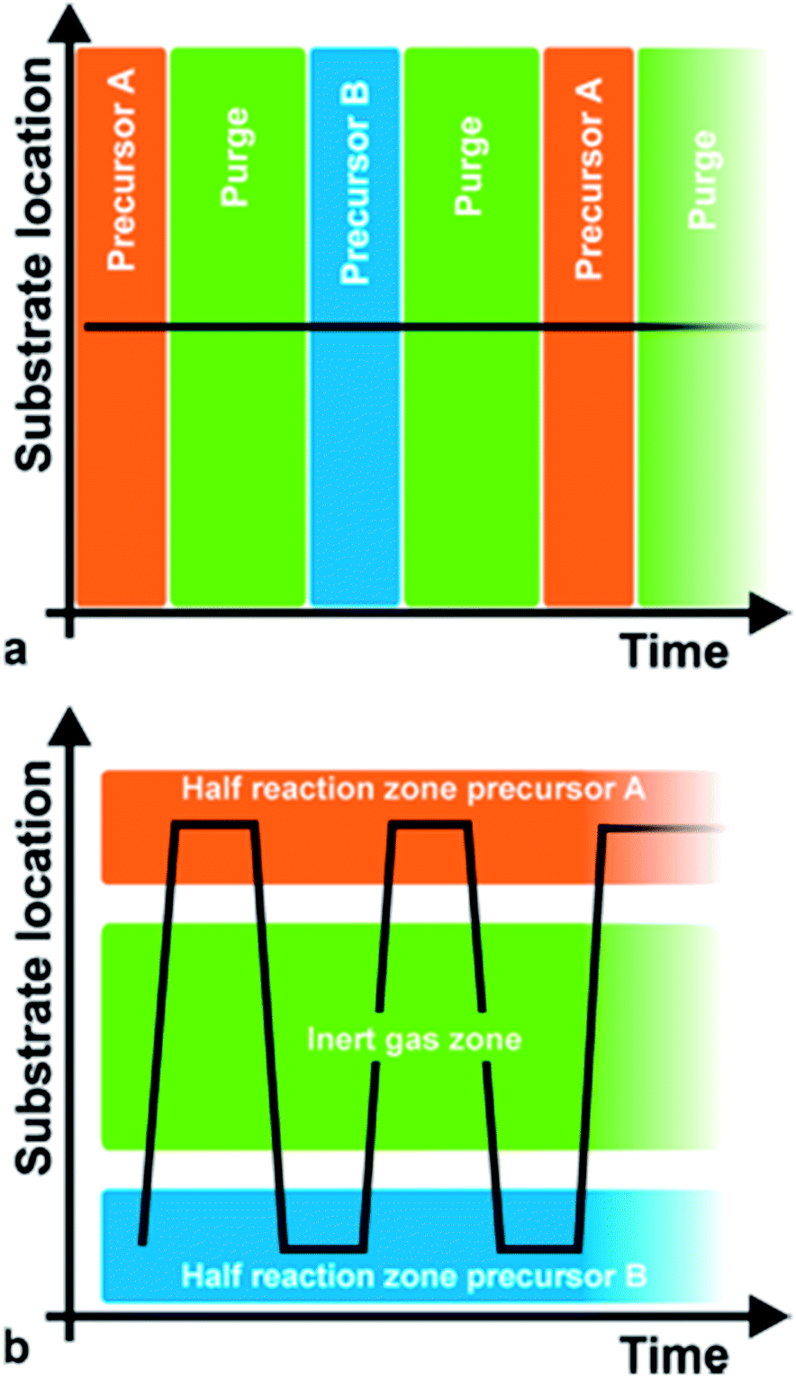 | ||
| Fig. 1 (a and b) Temporal vs. spatial ALD. Copyright 2011, AIP Publishing LLC; reprinted with permission from ref. 22. | ||
The key to atmospheric, high throughput ALD: from temporal to spatial
Although there have been several approaches to realizing ALD without the need of a high vacuum, Spatial ALD (SALD) has been the most popular in the last years due to its conceptual simplicity and the high deposition rates that can be achieved, and thus has also been called Atmospheric ALD (AALD).23 Conversely, atmospheric temporal ALD approaches based on fluidized reactors show comparable deposition rates with conventional vacuum ALD since those still rely on injection-purge cycles.24–27 The key idea allowing high throughput atmospheric spatial ALD is not new and was indeed patented in 1977 and 1983 by Suntola et al.28,29 It simply consists in separating the precursors in space rather than in time (Fig. 1b), as opposed to temporal ALD. Thus, in SALD the different precursors are supplied constantly in between inert gas regions. Films are then grown by alternatively exposing the substrate from one precursor region to the other going across the inert gas regions (Fig. 1b). In this way, the oscillation of the substrate (or of the gases injector) from one precursor zone to the second one, going across the inert gas regions, reproduces the classical temporal ALD scheme: the first metal precursor reacts with the surface forming a monolayer while any unreacted precursor is swept away and purged in the inert region; then the second precursor reacts with the previous monolayer forming a layer of material; finally the sample returns to the first precursor region again going across the inert region where any by-products and excess precursor are purged. This approach allows much faster deposition rates, which are mainly limited by the precursor reaction kinetics, so that a full reaction can take place while the sample is within the precursor zones. As recently reviewed by Poodt et al.,22 from 2008 there has been a variety of SALD designs exploiting this idea, some of them already being commercialized. The versatility of Suntola's approach can be appreciated by the multiple designs and configurations presented so far.22,30One of the approaches used in several of the recent SALD designs is the use of a short distance between the precursor delivery zone and the substrate (typically below 100 μm, Fig. 2a). In this configuration, referred to as “close proximity SALD”, the different gas regions are located along alternative channels where the gases flow parallel to each other, as illustrated in Fig. 2a. The close distance of the substrate, i.e. the small gap between injector and substrate, prevents the different precursors from mixing since the inert gas channel acts as an effective barrier. This approach has several advantages including: (i) the possibility of having smaller designs since the precursor regions are very small; (ii) simpler designs which are compatible with roll-to-roll processing; (iii) the possibility of using gas-bearings.22 Although several patents on close-proximity SALD were filed from 2008 to 2011,22 Levy et al. from Kodak were the first ones to present and publish their results on the deposition of ZnO thin film transistors, thus showing the suitability of SALD for fabricating device components.31 Later Poodt et al. also demonstrated high quality Al2O3 films obtained by SALD. These films were used to passivate the surface of conventional silicon solar cells.32 The design used by Levy et al. consists of a deposition head in which the different gas flows are distributed along the parallel channels (see scheme in Fig. 2b). This design is very simple and can be made very small, being indeed reminiscent of a printer head. Furthermore it is very easy to scale up, modify and customize. Finally, it is readily compatible with roll-to-roll processing. Such an approach is therefore very readily applicable both in laboratory and industrial settings. A similar approach has already been commercialized for the deposition of Al2O3 passivation layers on silicon and Cu(In, Ga)Se2 thin-film solar cells.22,33
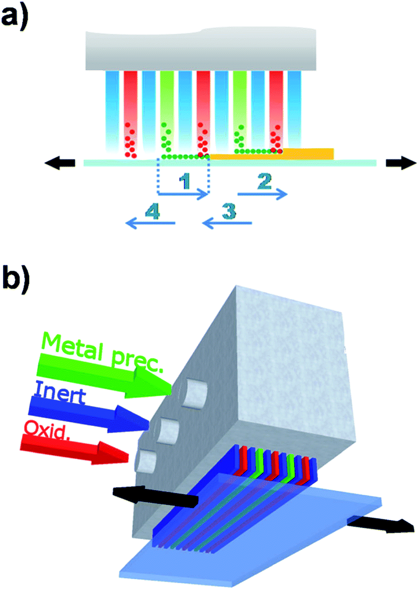 | ||
| Fig. 2 (a) Close-proximity SALD approach. The sample oscillates under the different flows reproducing the cycles in conventional ALD (numbered arrows); (b) scheme of the deposition head designed by Kodak. Copyright 2013 John Wiley & Sons, Ltd. Adapted with permission from ref. 23. | ||
The potential of SALD: fabrication of active components for low-cost solar cells
During the last years, in our group we have been using and developing a Kodak close-proximity SALD system, pioneering the deposition, study and implementation of high quality SALD films in low-cost/new generation photovoltaic devices.23,34–40 Our results include: (i) the demonstration of the feasibility of using SALD for the ultra-fast deposition of high-quality films that can be integrated in devices; (ii) the deposition of materials with superior properties compared to other low temperature and scalable methods; (iii) the fundamental studies of new-generation solar cells by using doped oxide films; and (iv) the nano-engineering of surfaces with SALD thin films to improve solar cells efficiencies. These results are succinctly reviewed next.In the first example we used SALD to grow high quality TiO2 blocking layers for organic (poly(3-hexylthiophene-2,5-diyl):[6,6]-phenyl-C61-butyric acid methyl ester (P3HT:PCBM)) solar cells.23 Dense, uniform thin TiO2 films were grown at temperatures as low as 100 °C in only 37 s (∼20 nm min−1 growth rate). Incorporation of these films in P3HT-PCBM-based solar cells showed performances comparable with cells made using TiO2 films deposited with much longer processing times and/or higher temperatures (SALD at 350 °C and spray pyrolysis at 450 °C). The high quality of the amorphous films obtained at 100 °C allowed the use of only 12 nm thick blocking layers, thus compensating for the lower conductivity of amorphous TiO2 with respect to crystalline TiO2, and resulting in two orders of magnitude faster deposition than other low-temperature scalable methods (Fig. 3a). We also studied thin ZnO (<200 nm) films grown by SALD in a matter of minutes as a hole-blocking layer in P3HT:PCBM based inverted solar cells. Despite the very rapid, open atmosphere growth method, the performances of the cells were comparable with the best cells of the same type reported in the literature. The performances were also maintained after 200 days of storage in air in the dark (Fig. 3b),34 showing the high stability of the ZnO films made by SALD.
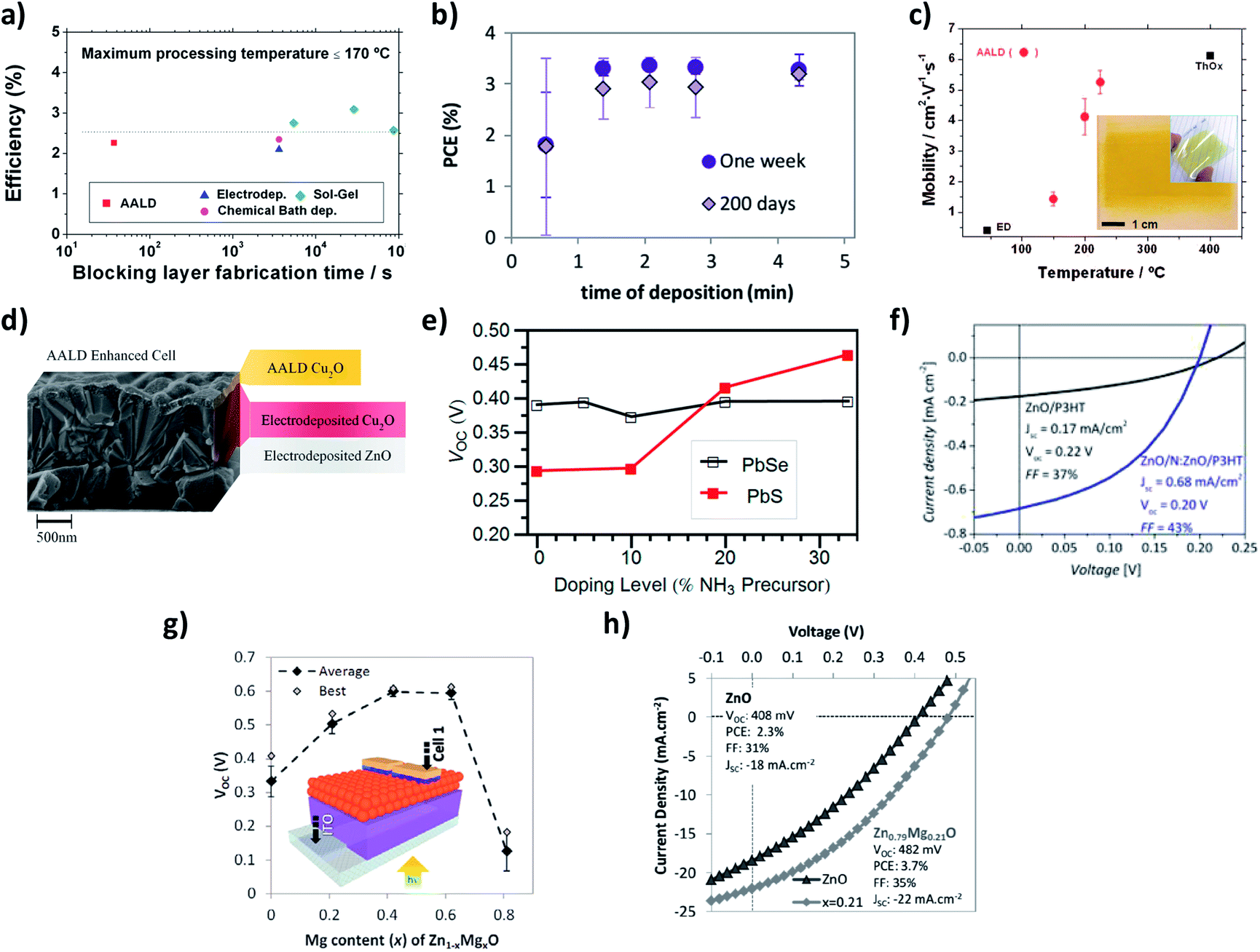 | ||
| Fig. 3 (a) Best SALD cell efficiency compared with equivalent cells from the literature in terms of blocking layer fabrication time; Copyright 2013 John Wiley & Sons, Ltd. Reprinted with permission from ref. 23. (b) Efficiency of devices with SALD ZnO hole-blocking layers measured one week after manufacture and 200 days after manufacture; Copyright 2013, Elsevier. Reprinted from ref. 34. (c) Mobility values as a function of temperature for SALD Cu2O films compared to reported values for other non-vacuum methods (ED: electrodeposition, ThOx: thermal oxidation); inset: optical photographs of Cu2O films deposited at 150 °C on 6.3 × 6.3 cm2 glass and flexible PEN substrates; Copyright 2012, American Institute of Physics. Licensed under Creative Commons Attribution 3.0 Unported. Reprinted from ref. 35. (d) Cross section SEM image of an SALD Cu2O-enhanced electrodeposited ZnO/Cu2O cell; Copyright 2013 Wiley-VCH Verlag GmbH & Co. KGaA. Reproduced with permission from ref. 36. (e) Open-circuit voltage of PbX (X = S, Se)/ZnO:N cells as a function of nitrogen-doping precursor fraction; Copyright 2013, American Chemical Society. Reprinted with permission from ref. 37. (f) Photovoltaic measurement of hybrid ZnO/P3HT devices employing approximately 60 nm ZnO films with and without a ZnO:N coating approximately 20 nm thick; Copyright 2014 Wiley-VCH Verlag GmbH & Co. KGaA. Reproduced with permission from ref. 39. (g) Open-circuit voltage (with device structure inset) for the Zn1−xMgxO/PbSe cells over a doping series. (h) Light J–V curves comparing the highest efficiency Zn1−xMgxO–PbSe CQDSC with the most efficient ZnO–PbSe CQDSC ones. Copyright 2013 Wiley-VCH Verlag GmbH & Co. KGaA. Reproduced from ref. 40. | ||
Secondly, we successfully deposited phase pure Cu2O films of thickness 50–120 nm using our SALD system at temperatures between 125 and 225 °C (Fig. 3c, inset).35 Growth rates were ∼1 nm min−1, which is two orders of magnitude faster than conventional ALD. The films grown at 225 °C had carrier mobility values above 5 cm2 V−1 s−1. Good carrier concentrations of around 1016 cm−3 were obtained for all deposition temperatures. The mobility values achieved were much higher than those obtained for electrodeposited films and approached the obtained for thermally oxidized films grown at 400 °C (Fig. 3c). Subsequently, we demonstrated SALD grown p+ Cu2O films on top of electrodeposited ZnO/Cu2O solar cells (Fig. 3d) to build in the electric field, thereby permitting the use of a thinner (∼1 mm compared to ∼3 mm) electrodeposited Cu2O layer. This thinner cell design gave reduced recombination losses and increased charge collection from both incident light and light reflected off the back electrode, resulting in a 29% increase in efficiency.36
Another of the advantages of SALD is that doping can be achieved very easily by adding precursors to the different precursor lines. As an example, nitrogen doped ZnO (ZnO:N) can be deposited by using an ammonia solution instead of water.41 N doping decreases the carrier concentration of ZnO and this has allowed us to perform fundamental studies of PbX (X = S, Se) quantum dot (QD)/ZnO solar cells. For QDs where there is a significant density of intragap states, recombination at the ZnO/QD interface can be limited by reducing the ZnO carrier concentration through N doping since it prevents the back-transfer of electrons and/or enables the collection of trapped electrons via sub-bandgap states in the ZnO. As a result, both the cell open circuit voltage (VOC) and efficiency increased with increasing N dopant level (Fig. 3e).37 We have also used SALD to engineer the surface of ZnO by depositing a 20 nm coating of N:ZnO on plain ZnO. The reduction in electron concentration in the surface results in enhanced exciton dissociation in ZnO/P3HT cells due to an improved light-induced de-trapping of electrons at the ZnO:N surface. This enhances exciton dissociation and electron transfer from the P3HT to the oxide, resulting in 4 times higher short circuit density (Fig. 3f).39 Finally, Mg doped ZnO has been successfully deposited using SALD, allowing a continuous tuning of the ZnO bandgap from 3.3 eV to 5.5 eV by adjusting the Mg percentage in Zn1−xMgxO. We then used Zn1−xMgxO in PbSe/ZnO solar cells, increasing the VOC from 408 mV up to 608 mV at a Zn1−xMgxO bandgap of 3.55 eV, the highest VOC reported to date for this type of cell (Fig. 3g and h).40
Future challenges for SALD: towards a materials printer
SALD is a technique that has only just recently begun to be used for the deposition of high quality materials in functional devices. Indeed, the first theoretical42–44 and kinetic45,46 studies on SALD have been published in just the last months and reports evaluating the effect of deposition conditions on the properties of SALD ZnO and Al2O3 were also published recently.47–49 To date, Al2O3, Cu2O, TiO2 and ZnO (including doping such as Al:ZnO, Mg:ZnO and ZnO:N) have already been demonstrated (Table 1 presents a summary of these materials and the application to solar cells detailed above). Hence, while it is early days, it is clear that there is tremendous potential for SALD, as briefly discussed in this minireview. The emergence and importance of SALD has also been recognized by the inclusion of a dedicated symposium on high throughput ALD at the AVS60 meeting (Fall 2013).| Material | Precursor | Growth rate/nm s−1 | Growth rate/nm per cycle | Deposition temperature/°C | Reactor | Sample size | Use in solar cells | Type of solar cell | Ref. |
|---|---|---|---|---|---|---|---|---|---|
| a Abbreviations: AZO: aluminium doped zinc oxide, TMA: tetramethyl aluminium, DEZ: diethyl zinc, L: laboratory system, n.t.: not tested in solar cells, Mg(CpEt)2: bis(ethylcyclopentadienyl)magnesium, TNO: Netherlands Organisation for Applied Scientific Research TNO, KCP: Kodak close proximity system; the growth rate per cycle refers to conventional ALD cycles, i.e. exposure to metal precursor followed by exposure to oxidant precursor. The relation between nn per cycle and nn per s depends both on each particular system and the deposition parameters used. | |||||||||
| AZO | TMA, DEZ | 0.20, 0.33 | 0.12, 0.2 | 200 | L:TNO circular | 3 cm | n.t. | 50 | |
| Al2O3 | TMA | 0.16 | 0.12 | 100 | L:web coater | 4 m × 100 mm | n.t. | 30 | |
| TMA | 1.20 | 0.12 | 200 | L:TNO circular | 3 cm | Barrier layer | Si, Cu(In, Ga)Se2 | 32 and 33 | |
| ZnO | DEZ | 0.90 | 0.18 | 75–250 | L:TNO circular | 3 cm | n.t. | 49 | |
| DEZ | 0.63 | 0.25 | 150 | L:KCP | Up to 15 cm2 | Hole blocking layer | Organic bulk heterojunction (P3HT/PCBM) | 34 | |
| Mg:ZnO | DEZ, Mg(CpEt)2 | 0.28 | 0.2 | 150 | L:KCP | Up to 15 cm2 | n-type | Quantum dot (ZnO/PbSe) | 40 |
| ZnO:N | DEZ, NH3 | 0.36 | 0.16 | 150 | L:KCP | Up to 15 cm2 | n-type | Quantum dot (ZnO/PbX, X = S, Se) | 37 |
| Hybrid (ZnO/P3HT) | 39 | ||||||||
| Cu2O | Cupraselect | 0.02 | 0.006 | 150–225 | L:KCP | Up to 15 cm2 | p-type, hole doping | Inorganic (ZnO/Cu2O) | 35 and 36 |
| TiO2 | TiCl4 | 0.32 | 0.15 | 100–350 | L:KCP | Up to 15 cm2 | Hole blocking layer | Organic bulk heterojunction (P3HT/PCBM) | 23 |
Despite this success, the ultimate challenge is to create a versatile materials printer based on the SALD approach where all the characteristics, materials and applications that are currently achievable with ALD can also be obtained with SALD, while maintaining the vacuum-free environment, use of simple equipment, and the orders of magnitude faster deposition rates. One of the main limitations of SALD compared to ALD is that only relatively high volatility precursors can be used in order to have a sufficient amount of precursor molecules in the carrier gas.
As the technique becomes more popular, we expect novel precursors to be designed specifically for SALD systems with higher volatility and reactivity. Of course, the price of novel SALD precursors will need to be reasonable in order not to compromise the low cost associated to SALD. But in this sense, SALD is intrinsically more efficient in terms of precursor utilisation, thus allowing the use of precursors with slightly higher prices than conventional ALD/CVD precursors. Other limitations that will have to be overcome include the ability to maintain the high deposition rates of SALD when high aspect ratio features have to be coated, since precursor diffusion plays a key role in these cases (particularly in the case of high aspect ratio cavities, such as supported alumina templates51,52). The coating of freeform samples will require novel SALD designs, especially in the case of the close proximity approach. Additionally, while plasmas have already been implemented in some SALD systems,22 their use in atmospheric systems will have to be developed by implementing atmospheric plasmas. Finally, the deposition of complex materials such as multicomponent oxides remains to be explored using SALD.
One of the main advantages of SALD is that it is based on a very simple idea that allows for freedom of design modification, and that it is a very simple and cost-effective research tool, implementable in many different laboratory settings. Thus, customized systems for specific materials or substrates will surely be developed in the coming years. We expect that over the next years we will see a proliferation in the utilization of SALD, both in terms of the number of system designs and applications targeted – the areas of flextronics and barrier layer coatings being primary examples.
Acknowledgements
DMR acknowledges funding from the Marie Curie Actions (FP7/2007-2013, grant agreement number 219332), the Ramon y Cajal 2011 programme from the Spanish MICINN and the European Social Fund, and the Comissionat per a Universitats i Recerca (CUR) del DIUE de la Generalitat de Catalunya, Spain. JLMD acknowledges the support of the European Research Council (ERC-2009-AdG 247276 NOVOX).References
- R. G. Gordon, in Atomic Layer Deposition for Semiconductors, ed. C. S. Hwang, Springer, 2013, p. 15 Search PubMed.
- T. Kääriäinen, D. Cameron, M.-L. Kääriäinen and A. Sherman, in Atomic Layer Deposition: Principles, Characteristics, and Nanotechnology Applicatons, Wiley-Scrivener, 2nd edn, 2013, p. 215 Search PubMed.
- W. M. M. (Erwin) Kessels and M. Putkonen, MRS Bull., 2011, 36, 907–913 CrossRef.
- G. N. Parsons, J. W. Elam, S. M. George, S. Haukka, H. Jeon, W. M. M. (Erwin) Kessels, M. Leskelä, P. Poodt, M. Ritala and S. M. Rossnagel, J. Vac. Sci. Technol., A, 2013, 31, 050818 Search PubMed.
- J. Ferguson, A. Weimer and S. George, Thin Solid Films, 2000, 371, 95–104 CrossRef CAS.
- E. Rauwel, O. Nilsen, P. Rauwel, J. C. Walmsley, H. B. Frogner, E. Rytter and H. Fjellvåg, Chem. Vap. Deposition, 2012, 18, 315–325 CrossRef CAS.
- M. Leskelä and M. Ritala, Thin Solid Films, 2002, 409, 138–146 CrossRef.
- M. Leskelä and M. Ritala, Angew. Chem., Int. Ed., 2003, 42, 5548–5554 CrossRef PubMed.
- R. L. Puurunen, J. Appl. Phys., 2005, 97, 121301 CrossRef PubMed.
- G. Clavel, E. Rauwel, M.-G. Willinger and N. Pinna, J. Mater. Chem., 2009, 19, 454 RSC.
- S. M. George, Chem. Rev., 2010, 110, 111–131 CrossRef CAS PubMed.
- V. Miikkulainen, M. Leskelä, M. Ritala and R. L. Puurunen, J. Appl. Phys., 2013, 113, 021301 CrossRef PubMed.
- M. Knez, K. Nielsch and L. Niinistö, Adv. Mater., 2007, 19, 3425–3438 CrossRef CAS.
- D. M. King, X. Liang and A. W. Weimer, Powder Technol., 2012, 221, 13–25 CrossRef CAS PubMed.
- C. Marichy, M. Bechelany and N. Pinna, Adv. Mater., 2012, 24, 1017–1032 CrossRef CAS PubMed.
- X. Meng, X.-Q. Yang and X. Sun, Adv. Mater., 2012, 24, 3589–3615 CrossRef CAS PubMed.
- M. Cassir, A. Ringuedé and L. Niinistö, J. Mater. Chem., 2010, 20, 8987 RSC.
- J. R. Bakke, K. L. Pickrahn, T. P. Brennan and S. F. Bent, Nanoscale, 2011, 3, 3482–3508 RSC.
- J. A. van Delft, D. Garcia-Alonso and W. M. M. Kessels, Semicond. Sci. Technol., 2012, 27, 074002 CrossRef.
- S. A. Skoog, J. W. Elam and R. J. Narayan, Int. Mater. Rev., 2013, 58, 113–129 CrossRef CAS PubMed.
- M. Ritala and M. Leskelä, in Handbook of Thin Film Materials, ed. H. S. Nalwa, Academic Press, 2002, pp. 103–159 Search PubMed.
- P. Poodt, D. C. Cameron, E. Dickey, S. M. George, V. Kuznetsov, G. N. Parsons, F. Roozeboom, G. Sundaram and A. Vermeer, J. Vac. Sci. Technol., A, 2012, 30, 010802 Search PubMed.
- D. Muñoz-Rojas, H. Sun, D. C. Iza, J. Weickert, L. Chen, H. Wang, L. Schmidt-Mende and J. L. MacManus-Driscoll, Progress in Photovoltaics: Research and Applications, 2013, 21, 393–400 Search PubMed.
- A. Hunter and A. H. Kitai, J. Cryst. Growth, 1988, 91, 111–118 CrossRef CAS.
- R. Beetstra, U. Lafont, J. Nijenhuis, E. M. Kelder and J. R. van Ommen, Chem. Vap. Deposition, 2009, 15, 227–233 CrossRef CAS.
- J. S. Jur and G. N. Parsons, ACS Appl. Mater. Interfaces, 2011, 3, 299–308 CAS.
- A. Goulas and J. Ruud van Ommen, J. Mater. Chem. A, 2013, 1, 4647 CAS.
- T. S. Suntola, A. J. Pakkala and S. G. Lindfors, 1983, US Pat., 4,389,973.
- T. S. Suntola and J. Antson, 1977, US Pat., 4,058,430.
- A. S. Yersak, Y. C. Lee, J. A. Spencer and M. D. Groner, J. Vac. Sci. Technol., A, 2014, 32, 01A130 Search PubMed.
- D. H. Levy, D. Freeman, S. F. Nelson, P. J. Cowdery-Corvan and L. M. Irving, Appl. Phys. Lett., 2008, 92, 192101 CrossRef PubMed.
- P. Poodt, A. Lankhorst, F. Roozeboom, K. Spee, D. Maas and A. Vermeer, Adv. Mater., 2010, 22, 3564–3567 CrossRef CAS PubMed.
- A. Illiberi, F. Grob, C. Frijters, P. Poodt, R. Ramachandra, H. Winands, M. Simor and P. J. Bolt, Progress in Photovoltaics: Research and Applications, 2013, 21, 1559–1566 CrossRef CAS.
- R. L. Z. Hoye, D. Muñoz-Rojas, D. C. Iza, K. P. Musselman and J. L. MacManus-Driscoll, Sol. Energy Mater. Sol. Cells, 2013, 116, 197–202 CrossRef CAS PubMed.
- D. Muñoz-Rojas, M. Jordan, C. Yeoh, A. T. Marin, A. Kursumovic, L. Dunlop, D. C. Iza, A. Chen, H. Wang and J. L. MacManus-driscoll, AIP Adv., 2012, 2, 042179 CrossRef PubMed.
- A. T. Marin, D. Muñoz-Rojas, D. C. Iza, T. Gershon, K. P. Musselman and J. L. MacManus-Driscoll, Adv. Funct. Mater., 2013, 23, 3413–3419 CrossRef CAS.
- B. Ehrler, K. P. Musselman, M. L. Böhm, F. S. F. Morgenstern, Y. Vaynzof, B. J. Walker, J. L. MacManus-Driscoll and N. C. Greenham, ACS Nano, 2013, 7, 4210–4220 CrossRef CAS PubMed.
- R. L. Z. Hoye, K. P. Musselman and J. L. MacManus-Driscoll, APL Mater., 2013, 1, 060701 CrossRef PubMed.
- K. P. Musselman, S. Albert-Seifried, R. L. Z. Hoye, A. Sadhanala, D. Muñoz-Rojas, J. L. Macmanus-Driscoll and R. H. Friend, Adv. Funct. Mater., 2014 DOI:10.1002/adfm.201303994.
- R. L. Z. Hoye, B. Ehrler, M. L. Böhm, D. Muñoz-Rojas, R. M. Altamimi, A. Y. Alyamani, Y. Vaynzof, A. Sadhanala, G. Ercolano, N. C. Greenham, R. H. Friend, J. L. MacManus-Driscoll and K. P. Musselman, Adv. Energy Mater., 2014 DOI:10.1002/aenm.201301544.
- L. Dunlop, A. Kursumovic and J. L. MacManus-Driscoll, Appl. Phys. Lett., 2008, 93, 172111 CrossRef PubMed.
- S. Suh, S. Park, H. Lim, Y.-J. Choi, C. S. Hwang, H. J. Kim and S.-J. Won, J. Vac. Sci. Technol., A, 2012, 30, 051504 Search PubMed.
- A. Holmqvist, T. Törndahl and S. Stenström, Chem. Eng. Sci., 2013, 96, 71–86 CrossRef CAS PubMed.
- C. D. Travis and R. A. Adomaitis, Chem. Vap. Deposition, 2013, 19, 4–14 CrossRef CAS.
- P. Poodt, J. van Lieshout, A. Illiberi, R. Knaapen, F. Roozeboom and A. van Asten, J. Vac. Sci. Technol., A, 2013, 31, 01A108 Search PubMed.
- P. Poodt, A. Illiberi and F. Roozeboom, Thin Solid Films, 2013, 532, 22–25 CrossRef CAS PubMed.
- M. B. M. Mousa, C. J. Oldham, J. S. Jur and G. N. Parsons, J. Vac. Sci. Technol., A, 2012, 30, 01A155 Search PubMed.
- P. Ryan Fitzpatrick, Z. M. Gibbs and S. M. George, J. Vac. Sci. Technol., A, 2012, 30, 01A136 Search PubMed.
- A. Illiberi, F. Roozeboom and P. Poodt, ACS Appl. Mater. Interfaces, 2012, 4, 268–272 CAS.
- A. Illiberi, R. Scherpenborg, Y. Wu, F. Roozeboom and P. Poodt, ACS Appl. Mater. Interfaces, 2013, 5, 13124–13128 CAS.
- X. Ren, T. Gershon, D. Iza, D. Muñoz-Rojas, K. Musselman and J. L. MacManus-Driscoll, Nanotechnology, 2009, 20, 365604 CrossRef CAS PubMed.
- K. P. Musselman, G. J. Mulholland, A. P. Robinson, L. Schmidt-Mende and J. L. MacManus-Driscoll, Adv. Mater., 2008, 20, 4470–4475 CrossRef CAS.
| This journal is © The Royal Society of Chemistry 2014 |