Growth of SnO2 nanosheet arrays on various conductive substrates as integrated electrodes for lithium-ion batteries†
Lei
Zhang
,
Hao Bin
Wu
and
Xiong (David)
Wen Lou
*
School of Chemical and Biomedical Engineering, Nanyang Technological University, 62 Nanyang Drive, Singapore 637459, Singapore. E-mail: xwlou@ntu.edu.sg; davidlou88@gmail.com; Web: http://www.ntu.edu.sg/home/xwlou/
First published on 26th September 2013
Abstract
A facile template-free solution method combined with a post annealing treatment is successfully developed to grow interconnected SnO2 nanosheets on various conductive substrates. Moreover, a second layer of SnO2 nanosheets can be grown on top of the first layer by simply repeating the procedure. When tested as integrated binder-free electrodes for lithium-ion batteries (LIBs), the electrodes deliver reasonably high specific capacity, excellent cycling stability and good rate capability.
Among the myriad energy-storage technologies, rechargeable lithium-ion batteries (LIBs) are currently the predominant power source for portable electronic devices, and have shown great promise for upcoming large-scale applications of electric vehicles, because of their advantages of high energy density, long lifespan, no memory effect, and environmental benignity.1–4 Tin dioxide (SnO2) has been regarded as a promising candidate as anode materials for LIBs based on the reversible alloying–dealloying reactions between lithium and metallic Sn nanocrystals, which can be described by the following equations:
| SnO2 + 4Li+ + 4e− → Sn + 2Li2O | (1) |
| Sn + xLi+ + xe− ↔ LixSn (0 ≤ x ≤ 4.4).5–8 | (2) |
The first reaction represents the largely irreversible reduction process of SnO2 to metallic Sn. Such an irreversible chemical transformation is partly responsible for the large initial irreversible capacity loss which is usually observed in SnO2-based electrodes.9–12 The second process illustrates the reversible alloying/dealloying process between Sn and Li, which contributes to the high theoretical specific capacity of ∼790 mA h g−1. However, this reversible process is also accompanied by a large volume change of more than 200%, which leads to pulverization of the electrodes and becomes one significant drawback of SnO2-based electrode materials.9–13 To improve the electrochemical performances of SnO2-based anodes, various nanostructured SnO2 materials with different shapes and particle sizes have been synthesized, including zero-dimensional (0D) nanoparticles,14,15 one-dimensional (1D) nanorods/nanowires/nanotubes,16–18 two-dimensional (2D) nanosheets,19,20 and three-dimensional (3D) hollow or porous nanostructures.21–27 It has been suggested that the low-dimensional such as 1D and 2D nanostructures are able to better withstand the huge volume change during the charge–discharge process.9–11,16–20 The void space provided by the hollow or porous structures can also accommodate the structural strain, thus leading to improved lithium storage properties.21–27 Notwithstanding these advances, the rational design and controllable synthesis of nanostructured SnO2 with superior lithium storage performance still remain as significant challenges.
Currently, an emerging new concept is to grow 3D electroactive nanostructures on conductive substrates to be directly used as integrated electrodes for LIBs.28,29 The 3D architectures not only ensure much higher lithium ion flux across the electrode due to the dramatically increased electrode–electrolyte interface, but also serve as the pathway for efficient electron transport. Moreover, the free space within 3D electrodes can better accommodate the volume variation of the entire electrode during lithium insertion/extraction.28,29 Therefore, significant improvements in electrochemical performance can be expected by using SnO2 nanostructures grown directly on conductive substrates. For example, Ko et al. reported the synthesis of SnO2 nanowires on the current collector based on a vapor–liquid–solid mechanism via a thermal evaporation method.30 The integrated single-crystalline SnO2 nanowire electrode demonstrates stable cycling behavior, high specific discharge capacity and superior rate capability. Wang et al. synthesized SnO2 nanotube arrays on a titanium substrate via ZnO nanowire arrays as sacrificial templates.31 The SnO2 nanotube arrays on the titanium substrate feature the large surface area, good electrical conductivity, and adhesion with the current collector, leading to the enhanced performance in LIBs. Liu et al. developed a hydrothermal approach to synthesize SnO2 nanorod arrays on large-area flexible metallic substrates (Fe–Co–Ni alloy and Ni foil), which delivers a high reversible capacity and excellent rate capability.32 Recently, Chen et al. reported a general kinetics-controlled solution growth of aligned mesocrystalline SnO2 nanorod arrays on several substrates for LIBs.33 The hydrolysis process of SnCl4 as well as the nucleation and growth of SnO2 crystals is delicately controlled in the mixed solvents, leading to an exclusively heterogeneous nucleation on the substrate and subsequent growth into mesocrystalline nanorod array. However, one common significant drawback of such integrated electrodes is the low mass loading of electroactive materials, which will limit the energy density of electrodes. In this work, a facile template-free solution method combined with a post annealing treatment is successfully developed to grow interconnected SnO2 nanosheets on various conductive substrates as integrated binder-free electrodes for LIBs. Importantly, a second layer of SnO2 nanosheets can be grown on top of the first layer by simply repeating this procedure. By growth of the SnO2 nanosheets double-layer, the mass loading of SnO2 nanosheets on the conductive substrate can be almost doubled, which provides an effective approach to increase the energy density of the integrated electrodes. These integrated electrodes deliver high specific capacity, excellent cycling stability and good rate capability.
Three different types of conductive substrates (i.e., Ti, Cu foil and flexible graphite paper) are used in this work. Take Ti foil as an example to illustrate the typical synthesis procedure. After the acid treatment to remove the possible impurities/oxide layer on the surface, the X-ray powder diffraction (XRD) pattern shows the high purity of Ti foil (Fig. S1, see ESI†). Interconnected SnO2 nanosheets are synthesized through a simple hydrothermal method coupled with a post-annealing treatment. The detailed preparation procedure can be found in the Experimental section. The crystallographic phase of the interconnected SnO2 nanosheets grown on Ti foil is determined by XRD as shown in Fig. 1. All of the diffraction peaks in the XRD pattern can be unambiguously assigned to tetragonal rutile SnO2 (JCPDS card no. 41-1445; space group P42/mnm, a0 = 4.738 Å, c0 = 3.187 Å) and Ti foil (JCPDS card no. 44-1294, Fig. S1, ESI†). No additional diffraction peaks from possible impurities are detected, indicating the high purity of the product. The optical photograph shows the brown surface color of the Ti foil after reaction, indicating the formation of the SnO2 layer (Fig. S2, ESI†).
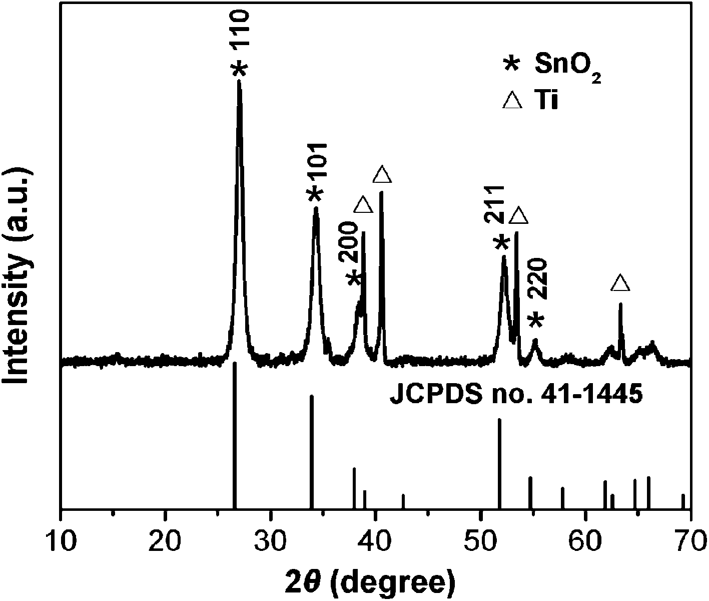 | ||
| Fig. 1 XRD pattern of SnO2 nanosheets double-layer on Ti foil. The standard pattern of SnO2 (JCPDS card no. 41-1445) is also provided for reference. | ||
Fig. 2a and b demonstrate the top-view field-emission scanning electron microscopy (FESEM) images of the interconnected SnO2 nanosheets single-layer grown on Ti foil. The panoramic FESEM image (Fig. 2a) shows that the SnO2 nanosheets are uniformly grown on Ti foil to form a conformal coating on the surface. The magnified FESEM image (Fig. 2b) reveals that the SnO2 layer is composed of perpendicularly oriented nanosheets. It can also be clearly observed that the open space between SnO2 nanosheets is relatively large and the SnO2 layer is constructed by interconnected sheet-like subunits with a thickness of several nanometers. Moreover, the SnO2 nanosheets are interconnected with each other to form a hierarchical network. The cross-section FESEM image shows the homogeneously aligned SnO2 nanosheets and that the thickness of the SnO2 nanosheets single-layer is about 250 nm (Fig. 2c). In average, the mass loading of the SnO2 nanosheets single-layer is about 0.4 mg on 1 cm2 of the conductive substrate.
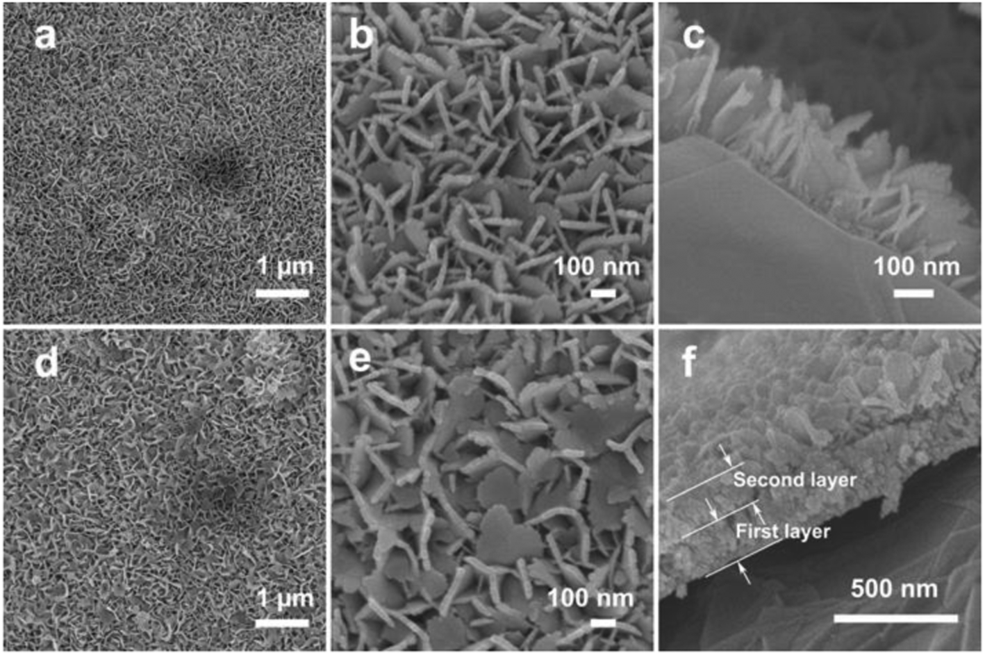 | ||
| Fig. 2 Top-view (a, b, d and e) and cross-section (c and f) FESEM images of SnO2 nanosheets single-layer (a–c) and double-layer (d–f) on Ti foil. | ||
By simply repeating the hydrothermal growth procedure on the SnO2 nanosheets single-layer as the substrate, a second layer of SnO2 nanosheets can be grown on top of the first layer to obtain SnO2 nanosheets double-layer on the conductive substrate. The low-magnification FESEM image shows that the second layer of SnO2 nanosheets is uniformly grown on the first SnO2 nanosheet layer to form a homogeneous coating on the first SnO2 nanosheet surface (Fig. 2d). The enlarged FESEM image shows that the sheet-like nanostructures of the second SnO2 nanosheet layer are as the same as that of the first SnO2 nanosheet layer (Fig. 2e). The cross-sectional FESEM image clearly shows the double-layered structure, and that the thickness of the second SnO2 layer is also about 250 nm (Fig. 2f), which is the same as the first layer. Thus, the total thickness of SnO2 nanosheets double-layer is about 500 nm. Moreover, the second SnO2 layer is robustly adhered to the first SnO2 layer and maintains the integrated structure. By growing SnO2 nanosheets double-layer on the conductive substrate, the mass loading of SnO2 nanosheets will be significantly increased to about 0.8 mg on 1 cm2 of the conductive substrate. Thus, a higher energy density of electrodes could be achieved by simply repeating the growth of a second layer of SnO2 nanosheets.
SnO2 nanosheets are scratched from Ti foil and further characterized by transmission electron microscopy (TEM) as shown in Fig. 3. The low-magnification image in Fig. 3a shows planar or perpendicular thin sheets, with the edge length mostly no more than 100 nm in both dimensions. The magnified image clearly shows that the nanosheets are continuous with a smooth surface (Fig. 3b). The high-resolution TEM (HRTEM) image of a flat lying nanosheet is shown in Fig. 3c. Lattice fringes with a spacing of 0.34 nm can be seen from the HRTEM image, corresponding to the (110) planes of SnO2. From the HRTEM observation of representative cross-sections of nanosheets (Fig. 3d), the thickness of SnO2 nanosheets is about 5 nm. The HRTEM image also shows a crystalline character with a lattice spacing of 0.24 nm, which is close to the interplanar distance of (111) planes of SnO2. Considering the crystallographic structure of SnO2, it might be deduced that the nominal exposed top and bottom planes of these nanosheets should be {111} facets, which is in agreement with that observed in a previous report.34
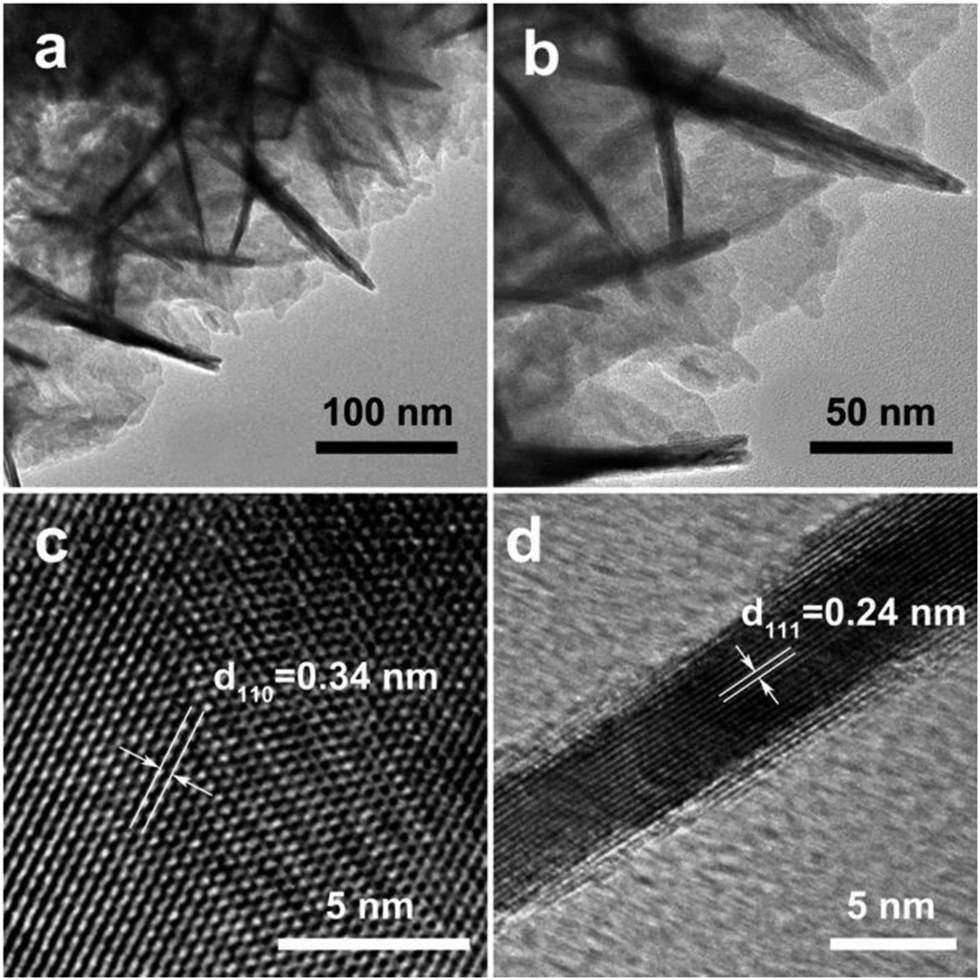 | ||
| Fig. 3 TEM (a and b) and HRTEM (c and d) images of SnO2 nanosheets scratched from Ti foil. | ||
Besides Ti foil, interconnected SnO2 nanosheets can also be well grown on other conductive substrates, such as Cu foil, and even flexible graphite paper, indicating the feasibility and generality of this facile method. As shown in Fig. 4 (also Fig. S2 and S3, see ESI†), SnO2 nanosheets single-layer and double-layer are successfully grown on Cu foil and graphite paper. The facile growth of SnO2 nanosheets on different substrates may endow promising applications in many fields. Moreover, it is worth noting that the successful growth of high-quality electroactive nanostructures on flexible substrates is very important for the fabrication of so-called wearable, light-weight or flexible energy-storage devices, which will find broad applications in many situations.
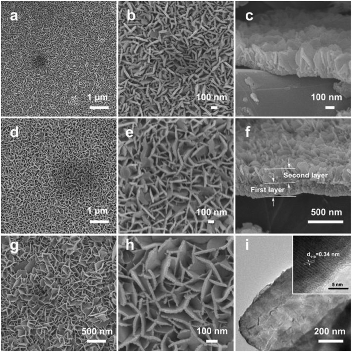 | ||
| Fig. 4 Top-view (a, b, d and e) and cross-section (c and f) FESEM images of SnO2 nanosheets single-layer (a–c) and double-layer (d–f) on graphite paper; top-view FESEM images (g and h), TEM (i) and HRTEM image (inset of i) of SnO2 nanosheets double-layer on Cu foil. | ||
Interconnected SnO2 nanosheets grown on Ti foil are directly used as an integrated electrode for LIBs to highlight the merits of the unique hierarchical structure. Fig. 5a shows the cyclic voltammograms (CV) of SnO2 nanosheets double-layer for the first three consecutive cycles at a scan rate of 0.5 mV s−1 in the voltage window of 2.5–0.005 V. The CV behavior is generally consistent with those of SnO2 reported in the literature, suggesting the same electrochemical reaction pathway.5–18,30–37 Specifically, three pairs of poorly defined redox current peaks can be clearly observed. The two apparent reduction peaks around 0.6 V and 0.7 V should be related to the partially reversible reduction of SnO2 to Sn (see eqn (1) above) and the formation of the solid–electrolyte interface (SEI), which shifts to a higher potential of about 0.9 V and 1.2 V after the first cycle.17 The other redox pair (cathodic, anodic) shown at the potentials (V) of (0.01, 0.7) can be attributed to the alloying (cathodic scan) and dealloying (anodic scan) processes (see eqn (2) above), which is much more pronounced than the other two pairs, marking the major contribution to the total capacity of the cell.30–37 From the second cycle onwards, the CV curves mostly overlap, indicating the good reversibility of the electrochemical reactions. In agreement with this CV result, the charge–discharge voltage profiles (Fig. S4 and S5, see ESI†) are characteristic of SnO2-based materials.5–18,30–37
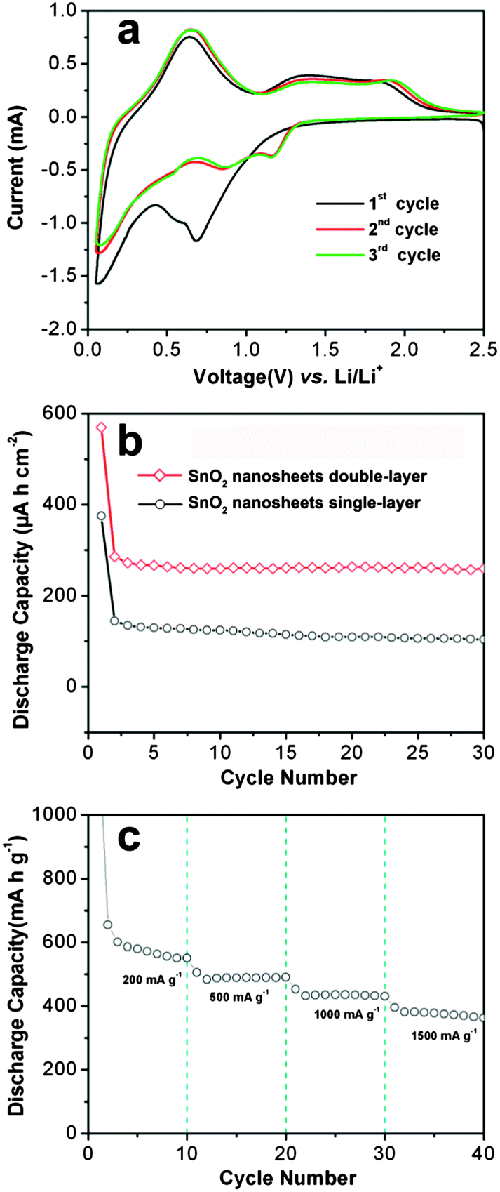 | ||
| Fig. 5 (a) CV profile of SnO2 nanosheets double-layer on Ti foil showing the first three cycles between 0.005 and 2.5 V at a scan rate of 0.5 mV s−1; (b) cycling performance of SnO2 nanosheets single-layer and double-layer on Ti foil over the voltage range of 0.05–1.5 V vs Li/Li+ at the same current density of 200 mA g−1; (c) rate capability of SnO2 nanosheets double-layer on Ti foil between 0.05 and 1.5 V. | ||
Fig. 5b shows the discharge–charge cycling performance of interconnected SnO2 nanosheets evaluated between 0.05 and 1.5 V at a current density of 200 mA g−1. The SnO2 nanosheets single-layer and double-layer deliver high initial discharge capacities of 375 and 570 μA h cm−2 (corresponding to and 1576 and 1196 mA h g−1), respectively. Clearly, there is a large capacity loss in the second cycle, which is mainly attributed to the initial irreversible formation of Li2O in the first cycle, and other irreversible processes such as trapping of some lithium in the lattice, inevitable formation of the SEI layer and electrolyte decomposition, which are common for most anode materials.5–18,30–37 From the second cycle onward, the two samples display excellent cycling stability with almost no fading of capacity over the first 30 cycles. In particular, the SnO2 nanosheet double-layer sample exhibits a high reversible capacity of 260 μA h cm−2 (∼550 mA h g−1; Fig. S5, ESI†) in the 30th cycle, whereas only a low capacity of 111 μA h cm−2 (∼500 mA h g−1; Fig. S4, ESI†) can be delivered by SnO2 nanosheets single-layer. It should be mentioned that the SnO2 nanosheet single-layer and double-layer electrodes show similar discharge capacities calculated based on the weight of SnO2 nanosheets (500–550 mA h g−1). Thus, the enhanced discharge capacity calculated when normalized with the surface area of integrated anodes is attributed to the high mass loading of SnO2 nanosheets in the double-layer sample (∼0.8 mg cm−2), which is almost twice that of the SnO2 nanosheets single-layer sample. By layer-by-layer growth of SnO2 nanosheets, the mass loading of electroactive materials on integrated electrodes could be increased. Thus, a high energy density of integrated electrodes for LIBs can be achieved. Compared with SnO2 nanosheets and nanoparticles,35,36 it is clear that the interconnected SnO2 nanosheets grown on Ti foil manifest significantly enhanced cycling performance. After cycling for 30 cycles, we have carried out the post-mortem study by FESEM examination (Fig. S6, see ESI†). Even though the SnO2 nanosheets are changed to SnO2 nanoparticles, the uniform interconnected SnO2 layer with open space between SnO2 nanoparticles can be still retained, indicating the good structural stability of this 3D integrated electrode and the unique nanostructure of interconnected SnO2 nanosheets. To evaluate the rate capability, the SnO2 nanosheets double-layer are cycled at various charge–discharge current densities ranging from 200 to 1500 mA g−1 over a voltage window of 0.05–1.5 V (Fig. 5c). The SnO2 nanosheet double-layer electrode experiences only small decrease in capacity as the current density increases. As an example, at a high current density of 1500 mA g−1, the SnO2 nanosheets double-layer can still deliver a stable discharge capacity of about 400 mA h g−1. Such a good rate performance is of great importance for fabricating LIBs with improved energy density for future high power applications.
The excellent cycling stability and rate capability of these SnO2-based integrated electrodes might be attributed to the combination of 3D integrated electrode and unique nanostructure of interconnected SnO2 nanosheets. Specifically, the ultrathin 2D sheet-like nanostructures possess a short distance for Li+ ion diffusion and large electrode–electrolyte contact area for high Li+ ion flux across the interface, leading to enhanced rate capability.19,20 Meanwhile, the low-dimensional 2D nanostructures can effectively accommodate the large volume change during the charge–discharge process, thus leading to improved lithium storage properties.19,20 Also, the interconnected SnO2 nanosheet array maintains all the advantageous features of building 2D nanostructure arrays on conductive metal substrates, such as the short diffusion length and facile strain relaxation, good structural buffer against volume change offered by the interval space between interconnected SnO2 nanosheets, and fast electron transport owing to the robust adhesion of arrayed nanosheets to the conductive substrates and their large contact area with the electrolyte.28,29 Combining the low-dimensional 2D sheet-like nanostructures, the 3D integrated electrode, and layer-by-layer growth of electroactive materials, the integrated electrode design of interconnected SnO2 nanosheets grown on conductive substrates offers another promising route for improving the cycle life and energy density of SnO2-based electrodes for LIBs.
In summary, we have rationally designed and grown interconnected SnO2 nanosheets on various conductive substrates as integrated binder-free electrodes for lithium-ion batteries. Moreover, a second layer of SnO2 nanosheets can be grown on top of the first layer of SnO2 nanosheets by simply repeating the growth procedure, which provides an effective approach to increase the energy density of the integrated electrodes. The obtained integrated electrode manifests high specific capacity, excellent cycling stability and good rate capability. Such highly integrated binder- and additive-free electrodes made by directly growing electroactive nanostructured materials on conductive substrates might hold some potential to develop a new class of high-performance electrodes for high-energy lithium-ion batteries.
Experimental section
Materials synthesis
In a typical synthesis, a conductive substrate (graphite paper, Ti or Cu foil, 2 cm × 4 cm in rectangular shape) was immersed in a 3 M HCl solution for 5 min to clear the surface layer before reaction. Urea (Sigma-Aldrich, 0.5 g), mercaptoacetic acid (Sigma-Aldrich, 10 μL), and HCl solution (37 wt%, Merck, 0.5 mL) were dissolved into 40 mL of H2O at room temperature to form a clear solution, followed by the addition of tin dichloride dehydrate (SnCl2·2H2O; Sigma-Aldrich, 0.1 g). After stirring for 2 min, the reaction mixture was then transferred into a 60 mL polytetrafluoroethylene (Teflon)-lined stainless-steel autoclave, and the pretreated conductive substrate was placed in the autoclave. Afterwards, the autoclave was heated to 120 °C in an electric oven. After reaction for 6 h, the substrate was taken out and then cleaned by ultrasonication to remove the loosely attached products on the surface before being fully dried in air at 60 °C. To grow a second SnO2 nanosheet layer on the conductive substrate, the same procedure was repeated by using the conductive substrate with SnO2 nanosheets single-layer. In order to get crystallized SnO2 sheets, the conductive substrate with the as-grown precursor was annealed in N2 at 500 °C with a temperate ramp of 1 °C min−1 for 6 h. The mass loadings of SnO2 were calculated based on the weight difference before and after growth of SnO2. 10 pieces of conductive substrates were weighed to calculate the average mass loadings of SnO2. In average, the mass loading of the SnO2 nanosheets single-layer is ∼0.4 mg on 1 cm × 1 cm of the conductive substrate, carefully weighed after calcination. By growing SnO2 nanosheets double-layer on the conductive substrate, the loaded amount of SnO2 nanosheets is increased to ∼0.8 mg on 1 cm × 1 cm of the conductive substrate.Materials characterization
X-ray diffraction (XRD) patterns were collected on a Bruker D8 Advanced X-ray Diffractometer with Ni filtered Cu Kα radiation (λ = 1.5406 Å) at a voltage of 40 kV and a current of 40 mA. Field-emission scanning electron microscopy (FESEM) images were acquired on a JEOL JSM 6700F microscope operated at 5 kV. Transmission electron microscopy (TEM) images were taken on JEOL 2010 and JEOL 2100F microscopes.Electrochemical measurements
The electrochemical tests were carried out using two-electrode Swagelok-type cells with pure lithium foil as the counter and reference electrodes at room temperature. The conductive substrate supported SnO2 nanosheets were directly applied as the working electrode without an ancillary binder or conductive agent. The electrolyte was 1.0 M LiPF6 in a 50![[thin space (1/6-em)]](https://www.rsc.org/images/entities/char_2009.gif) :50 (w/w) mixture of ethylene carbonate and diethyl carbonate. Cell assembly was carried out in an Ar-filled glovebox with both moisture and oxygen concentrations below 1.0 ppm. The galvanostatic charging–discharging tests were performed on a NEWARE battery tester with a cut-off voltage window of 0.05–1.5 V vs. Li+/Li.
:50 (w/w) mixture of ethylene carbonate and diethyl carbonate. Cell assembly was carried out in an Ar-filled glovebox with both moisture and oxygen concentrations below 1.0 ppm. The galvanostatic charging–discharging tests were performed on a NEWARE battery tester with a cut-off voltage window of 0.05–1.5 V vs. Li+/Li.
References
- J. M. Tarascon and M. Armand, Nature, 2001, 414, 359–367 CrossRef CAS PubMed.
- Y. K. Sun, Z. H. Chen, H. J. Noh, D. J. Lee, H. G. Jung, Y. Ren, S. Wang, C. S. Yoon, S. T. Myung and K. Amine, Nat. Mater., 2012, 11, 942–947 CrossRef CAS PubMed.
- F. Y. Cheng, J. Liang, Z. L. Tao and J. Chen, Adv. Mater., 2011, 23, 1695–1715 CrossRef CAS PubMed.
- Y. J. Zhang, Z. Schnepp, J. Y. Cao, S. X. Ouyang, Y. Li, J. H. Ye and S. Q. Liu, Sci. Rep., 2013, 3, 2163 Search PubMed.
- Y. Idota, T. Kubota, A. Matsufuji, Y. Maekawa and T. Miyasaka, Science, 1997, 276, 1395–1397 CrossRef CAS.
- R. Demir-Cakan, Y. S. Hu, M. Antonietti, J. Maier and M. M. Titirici, Chem. Mater., 2008, 20, 1227–1229 CrossRef CAS.
- D. Deng, M. G. Kim, J. Y. Lee and J. Cho, Energy Environ. Sci., 2009, 2, 818–837 CAS.
- X. S. Zhou, L. J. Wan and Y. G. Guo, Adv. Mater., 2013, 25, 2152–2157 CrossRef CAS PubMed.
- J. S. Chen and X. W. Lou, Mater. Today, 2012, 15, 246–254 CrossRef CAS.
- J. S. Chen and X. W. Lou, Small, 2013, 9, 1877–1893 CrossRef CAS PubMed.
- H. B. Wu, J. S. Chen, H. H. Hng and X. W. Lou, Nanoscale, 2012, 4, 2526–2542 RSC.
- L. W. Ji, Z. Lin, M. Alcoutlabi and X. W. Zhang, Energy Environ. Sci., 2011, 4, 2682–2699 CAS.
- D. Larcher, S. Beattie, M. Morcrette, K. Edstroem, J. C. Jumas and J. M. Tarascon, J. Mater. Chem., 2007, 17, 3759–3772 RSC.
- W. M. Zhang, J. S. Hu, Y. G. Guo, S. F. Zheng, L. S. Zhong, W. G. Song and L. J. Wan, Adv. Mater., 2008, 20, 1160–1165 CrossRef CAS.
- K. T. Lee, Y. S. Jung and S. M. Oh, J. Am. Chem. Soc., 2003, 125, 5652–5653 CrossRef CAS PubMed.
- L. Zhang, G. Q. Zhang, H. B. Wu, L. Yu and X. W. Lou, Adv. Mater., 2013, 25, 2589–2593 CrossRef CAS PubMed.
- M. S. Park, G. X. Wang, Y. M. Kang, D. Wexler, S. X. Dou and H. K. Liu, Angew. Chem., Int. Ed., 2007, 46, 750–753 CrossRef CAS PubMed.
- Y. Wang, H. C. Zeng and J. Y. Lee, Adv. Mater., 2006, 18, 645–649 CrossRef CAS.
- C. Wang, G. H. Du, K. Stahl, H. X. Huang, Y. J. Zhong and J. Z. Jiang, J. Phys. Chem. C, 2012, 116, 4000–4011 CAS.
- J. S. Chen, M. F. Ng, H. B. Wu, L. Zhang and X. W. Lou, CrystEngComm, 2012, 14, 5133–5136 RSC.
- X. W. Lou, L. A. Archer and Z. C. Yang, Adv. Mater., 2008, 20, 3987–4019 CrossRef CAS.
- X. W. Lou, C. M. Li and L. A. Archer, Adv. Mater., 2009, 21, 2536–2539 CrossRef CAS.
- X. W. Lou, Y. Wang, C. L. Yuan, J. Y. Lee and L. A. Archer, Adv. Mater., 2006, 18, 2325 CrossRef CAS.
- Z. Y. Wang, L. Zhou and X. W. Lou, Adv. Mater., 2012, 24, 1903–1911 CrossRef CAS PubMed.
- J. Fan, T. Wang, C. Z. Yu, B. Tu, Z. Y. Jiang and D. Y. Zhao, Adv. Mater., 2004, 16, 1432–1436 CrossRef CAS.
- S. J. Han, B. C. Jang, T. Kim, S. M. Oh and T. Hyeon, Adv. Funct. Mater., 2005, 15, 1845–1850 CrossRef CAS.
- Z. H. Wen, Q. Wang, Q. Zhang and J. H. Li, Adv. Funct. Mater., 2007, 17, 2772–2778 CrossRef CAS.
- J. Jiang, Y. Y. Li, J. P. Liu, X. T. Huang, C. Z. Yuan and X. W. Lou, Adv. Mater., 2012, 24, 5166–5180 CrossRef CAS PubMed.
- B. Liu, X. F. Wang, H. T. Chen, Z. R. Wang, D. Chen, Y. B. Cheng, C. W. Zhou and G. Z. Shen, Sci. Rep., 2013, 3, 1622 Search PubMed.
- Y. D. Ko, J. G. Kang, J. G. Park, S. Lee and D. W. Kim, Nanotechnology, 2009, 20, 455701 CrossRef PubMed.
- J. Z. Wang, N. Du, H. Zhang, J. X. Yu and D. R. Yang, J. Phys. Chem. C, 2011, 115, 11302–11305 CAS.
- J. P. Liu, Y. Y. Li, X. T. Huang, R. M. Ding, Y. Y. Hu, J. Jiang and L. Liao, J. Mater. Chem., 2009, 19, 1859–1864 RSC.
- S. Chen, M. Wang, J. F. Ye, J. G. Cai, Y. R. Ma, H. H. Zhou and L. M. Qi, Nano Res., 2013, 6, 243–252 CrossRef CAS.
- H. B. Wu, J. S. Chen, X. W. Lou and H. H. Hng, J. Phys. Chem. C, 2011, 115, 24605–24610 CAS.
- S. J. Ding and X. W. Lou, Nanoscale, 2011, 3, 3586–3588 RSC.
- S. J. Ding, D. Y. Luan, F. Y. C. Boey, J. S. Chen and X. W. Lou, Chem. Commun., 2011, 47, 7155–7157 RSC.
- Q. Kuang, T. Xu, Z. X. Xie, S. C. Lin, R. B. Huang and L. S. Zheng, J. Mater. Chem., 2009, 19, 1019–1023 RSC.
Footnote |
| † Electronic supplementary information (ESI) available. See DOI: 10.1039/c3mh00077j |
| This journal is © The Royal Society of Chemistry 2014 |