Production of heavily n- and p-doped CVD graphene with solution-processed redox-active metal–organic species†
Sergio A.
Paniagua
a,
Jose
Baltazar
b,
Hossein
Sojoudi
c,
Swagat K.
Mohapatra‡
a,
Siyuan
Zhang
a,
Clifford L.
Henderson
b,
Samuel
Graham
c,
Stephen
Barlow
a and
Seth R.
Marder
*a
aSchool of Chemistry and Biochemistry and Center for Organic Photonics and Electronics, Georgia Institute of Technology, Atlanta, GA 30332-0400, USA. E-mail: seth.marder@chemistry.gatech.edu
bSchool of Chemical and Biomolecular Engineering, Georgia Institute of Technology, Atlanta, GA 30332-0100, USA
cWoodruff School of Mechanical Engineering and Center for Organic Photonics and Electronics, Georgia Institute of Technology, Atlanta, GA 30332-0405, USA
First published on 3rd September 2013
Abstract
CVD graphene has been n- and p-doped using redox-active, solution-processed metal–organic complexes. Electrical measurements, photoemission spectroscopies, and Raman spectroscopy were used to characterise the doped films and give insights into the changes. The work function decreased by as much as 1.3 eV with the n-dopant, with contributions from electron transfer and surface dipole, and the conductivity significantly increased.
Adsorption of dopants onto graphene can be used to tailor its electrical properties1 by increasing the number of charge carriers2 and/or opening a band gap.3 A potential application for chemical-vapour-deposited (CVD) graphene is as transparent conductive electrodes,4 performance of which in organic electronic devices already rivals that of ITO.5,6 Doping can be used to modulate the work function (WF) and decrease the sheet resistance by introduction of charge carriers, thus potentially lowering contact resistances and leading to further improvements.7 Although adsorption of gases can lead to n- or p-doping8 through charge-transfer complex formation,9 the interaction is rather weak,10 and dedoping can readily occur.11 Alkali metals deposited in vacuum n-dope graphene, but can cause damage,12 while the resulting metal cations act as charge scatterers that significantly reduce the mobility.13
Molecules that form large, stable ions are potentially advantageous over alkali-metal ions since their lower charge densities decrease their ability to act as electrostatic charge traps. One of the most effective n-dopants used to date for graphene doping is an air-stable benzoimidazole derivative (MeO-DMBI), which gives a significant increase in conductivity and a WF decrease of 0.7 eV.14 The most widely used p-dopant has been 2,3,5,6-tetrafluoro-7,7,8,8-tetracyanoquinodimethane (F4-TCNQ, with an electron affinity, EA, of 5.24 eV15), generally vapour-deposited. An increase in WF of 1.3 eV has been reported for epitaxial graphene on SiC.16 However, F4-TCNQ is very volatile, interdiffuses in organic films,17 and is poorly soluble.
We have recently reported that the essentially air-stable dimers of certain organometallic compounds act as “masked” forms of the highly reducing monomers, readily losing two electrons to form two monomeric cations.18,19 We were interested in doping graphene with these dimers since the H˙ (or H−) transfer reactions possible for MeO-DMBI alongside, or in competition with, electron transfer are not anticipated; moreover, the dimers are known to be considerably stronger reductants, n-doping materials with EAs as low as ca. 3.0 eV through both vacuum and solution processing.
Here we use one of the above-mentioned dimers, 12,20,21 to n-dope CVD graphene films. The thermodynamics of doping depend on the strength of the dimer's central C–C bond and the monomer's ionisation potential (IP). The bond in 12 is estimated from experiment (ΔGdiss(12) < 0.24 eV) and theory to be particularly weak,21 meaning that, although the solid-state IP of 12 is estimated to be ca. 3.8 eV, the estimated IP of 1 (2.7 eV, ESI†) is a better gauge of its reducing ability. We also use a more soluble analogue of molybdenum tris-[1,2-bis(trifluoromethyl)ethane-1,2-dithiolene], Mo(tfd)3 – the new compound 2 (ESI†) – to p-dope graphene, since it offers the advantages of larger size, lower volatility, and higher electron affinity (5.6 eV) than F4-TCNQ.22,23 In both cases, we use multiple techniques to confirm doping and to understand the phenomena observed. Chemical structures and estimated energy levels are shown in Fig. 1.
 | ||
| Fig. 1 Schematic representation of n- and p-doping of graphene by 12 (in equilibrium with 1, 10 min dip) and 2 (overnight dip), with associated energy levels. IP, EA and WF (ϕ) values were estimated from electrochemical and UPS data (ESI†). The pristine graphene ϕ depended on the batch (4.1 eV for the sample before n-doping and 3.9 eV before p-doping). After treatment, the ϕ is affected by electron transfer (ET) between dopant and graphene, shifting the Fermi level (EF) relative to the Dirac point (ED), and the induced surface dipoles (SD) from the resulting charges, which change the local vacuum level (VL). | ||
As explained in detail in the ESI,† all sample modifications and characterizations were done without exposure to air. CVD-grown graphene was transferred onto patterned SiO2 and annealed inside a glovebox until the neutrality point (VNP) was zero (from here on referred to as pristine). Samples were then exposed to toluene solutions of dopants for various times, followed by rinsing with additional toluene to remove any weakly physisorbed material. Fig. 2 shows the transfer characteristics of a back-gated/bottom-contact graphene field-effect transistor (GFET) before and after successive treatments with 12. A short immersion time (ca. 1 s) in a low concentration solution (0.025 mM) gave a significant shift of the neutrality point to negative voltage (VNP = −66 V), consistent with n-doping. Eqn (1) was used to estimate the electron density in the conduction band,24n, from VNP and the capacitance per unit area of the gate dielectric (300 nm SiO2, CG = 115 aF μm−2), resulting in a value of n = 4.7 × 10¹² e cm−2.
 | (1) |
 | ||
| Fig. 2 GFET transfer characteristics before and after treatment with 12. The initial on/off ratio (black) and relative increases in current at VG = 0 are shown as dashed lines (VDS = 0.1 V). | ||
Longer treatments (10 s, 10 min) on the same sample with a 2.5 mM solution gave slight additional increases in conductivity (at VG = 0 V), but the neutrality point was no longer observable due to the −100 V limit imposed by the dielectric, precluding determination of n from eqn (1). The increase in conductivity appears to be limited by the on/off ratio of the pristine graphene.
X-ray photoelectron spectroscopy (XPS) was used to investigate the number and nature of dopant-related species present on the surface (without exposure of the samples to air). The ratio of the area of the Rh 3d3/2 and 3d5/2 core ionisations (Fig. 3a) to that of the graphene C 1s peak was used to estimate the surface coverage. A close-packed monolayer of 1+ cations, with their principal axes oriented perpendicular to the graphene surface, is estimated to correspond to ca. 1 Rh atom per 28 graphene carbons (ESI†). The data for the sample dipped in dilute solution suggests ca. 3% of a monolayer, whereas that for samples exposed to 2.5 mM suggest 25% and 75% of a monolayer for 10 s and 10 min immersions respectively (ESI†).
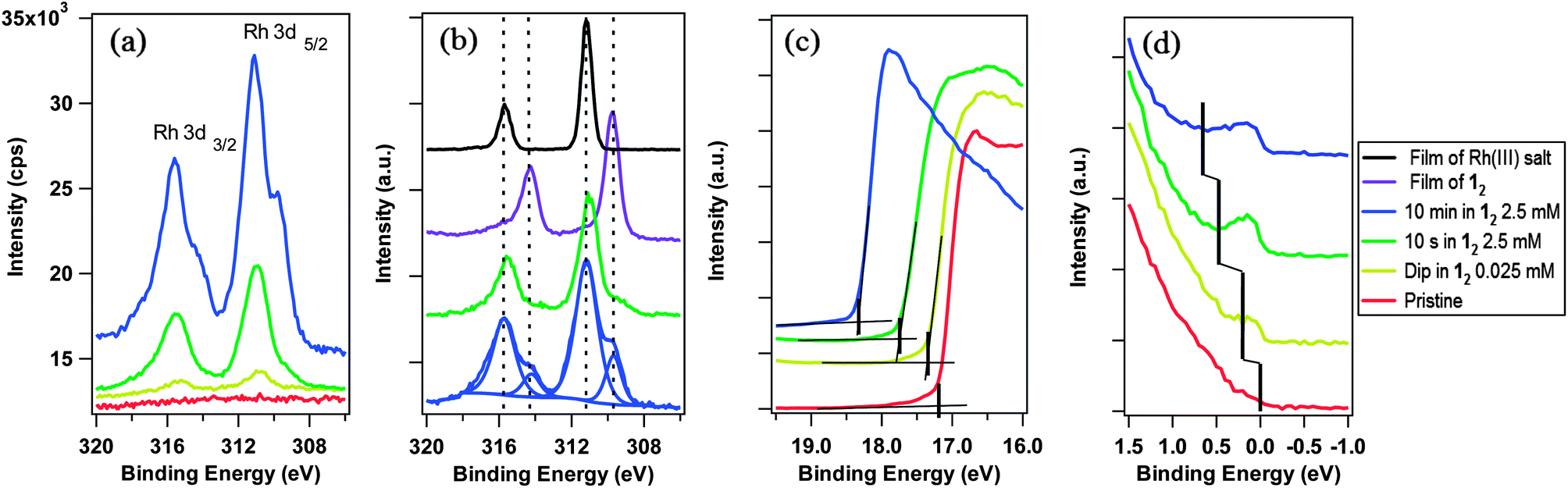 | ||
| Fig. 3 XPS/UPS spectra for pristine and 12-treated graphene. (a) Rh 3d XPS regions, (b) comparison with thick films of 12 and 1+PF6−. Peak fits are shown for graphene treated for 10 min. (c) Representative UPS secondary electron edges for WF determination and (d) UPS valence band region used to track changes in ED–EF. The feature seen close to BE = 0 eV for the doped samples in (d) is attributed to ionisation of electrons from the graphene conduction band, and the minimum in photoemission (marked with a vertical black line) is attributed to the Dirac point. Traces offset vertically for clarity in (b)–(d). | ||
Furthermore, while the sample treated by dipping in dilute solution shows a single pair of Rh 3d ionisations with a 3d5/2 binding energy (BE) of 310.8 eV, increasing exposure of the same sample to 12 leads to the emergence of significant shoulders at lower BE; the lower energy component has an area 23% that of the higher BE component for the sample treated with 2.5 mM 12 for 10 s and 40% in the case of the 10 min sample. Comparison (Fig. 3b) of these signals with XPS data for dropcast films (on SiO2) of 1+PF6− (RhIII) and 12 (RhI) strongly suggest that the higher BE component is attributable to 1+, the expected product of doping, and that the lower BE species is unreacted 12. Thus, after short treatments most of the deposited species appear to be 1+, generated by electron transfer to graphene (as shown in Fig. 1). With increased extent of doping, 12 becomes less reactive towards the substrate, presumably due to band filling, changes in surface dipole, and the electrostatic effect of other 1+ cations already present at the surface, but apparently strongly physisorbs to the graphene. Since the dopant coverages are on the order of a monolayer, the transparency of graphene is maintained at over 95% through the visible region (ESI†); this can be contrasted to some other approaches to graphene doping.25
UV photoelectron spectroscopy (UPS) was used to determine the WF (ϕ = 21.22 eV – ESEE, where SEE denotes the secondary electron edge, Fig. 3c) and position of the Dirac point (ED) relative to the Fermi level (EF, Fig. 3d); the results are summarised in Fig. 4a as a function of adsorbed RhIII (from XPS). The pristine sample used for n-doping had a WF of 4.10 ± 0.08 eV, and the valence band section of the spectrum showed emission extending all the way to EF (BE = 0). The WF decreases slightly (−0.26 eV) with the quick exposure to dilute solution, with a slight dip in the emission at a BE = 0.2 eV, which we attribute to the Dirac point, now shifted relative to EF (still aligned with the spectrometer, at BE = 0) due to filling of the graphene conduction band by electron transfer from 12. 10 s treatment with the 2.5 mM solution leads to a further decrease in WF (−0.66 eV relative to pristine) with a clearly observable Dirac point at BE = 0.5 eV. A 10 min treatment with the concentrated solution gave an additional decrease of −1.29 eV to render a WF of 2.81 ± 0.06 eV, with ED − EF = 0.7 eV. To the best of our knowledge, this is the largest decrease in WF reported for graphene using adsorbed molecular dopants (see ESI† for comparison to some other graphene surface treatments). The contribution to the WF change from filling of the conduction band, ΔϕET = ED − EF, was used to determine the number of charge carriers, n, introduced according to eqn (2) (derived using the band structure of graphene near the K point; νF is the Fermi velocity, ħνF = 5.52 eV Å).26,27 The results are shown in Fig. 4b and compared with XPS estimates, which assume formation of each 1+ cation is accompanied by transfer of one electron to graphene. In general, the UPS and XPS estimates are in good agreement. Moreover, the value of n estimated from eqn (2) for the short immersion in dilute solution,27 (4 ± 1) × 1012 cm−2, agrees well with that obtained from GFET data viaeqn (1) (4.7 × 1012 cm−2).
 | (2) |
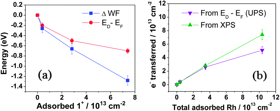 | ||
| Fig. 4 (a) Change in WF and ED (relative to EF) with increase in adsorbed 1+. (b) Charge-carrier density n calculated from eqn (2) using ED–EF (from UPS) compared with estimation from the number of RhIII species present (from XPS). | ||
While the changes in ED − EF can be attributed to band filling, Fig. 4a shows that the change in WF is larger than ΔϕET, consistent with what has previously been seen for some dopants on graphene.16,28,29 This difference can be attributed to the surface dipole resulting from the formation of a layer of 1+ cations on top of a negatively charged graphene sheet, which will contribute ΔϕSD to the total WF change, as shown in eqn (3), where q(z) and εr(z) describe the variation in charge density and effective dielectric constant along the direction normal to the surface.
 | (3) |
Without a detailed knowledge of q(z) and εr(z), we cannot evaluate the integral, but the model is broadly consistent with our data under certain assumptions (see ESI†). Qualitatively, the increasing importance of ΔϕSD relative to ΔϕET (Fig. 4a) is consistent with their predicted respective n and n1/2 dependencies. For the quick-dip sample the WF change is almost entirely due to ΔϕET (ED − EF), whereas in the most heavily doped case the two contributions are of comparable magnitude, as shown schematically on the left side of Fig. 1.
Raman spectra were also acquired without exposure to air30 (Fig. 5a) and compared with data acquired in situ with heavy electrical doping.27,31 The significant decrease in the intensity ratio of the 2D and G peaks (Fig. 5b), the increase of the G peak position, and the decrease in 2D peak position observed after treatment with 12 (Fig. 5c) are all consistent with strong n-doping. By comparing the G peak shift (Fig. 5d) with experimental plots from ref. 27 and 31, the charge-carrier concentration, n, was estimated as ∼5 × 1012 cm−2 for the quick dip in dilute solution (in accordance with our GFET data), and >2 × 1013 cm−2 for successive treatments, again in agreement with the values inferred from photoemission spectroscopy. The values of n for the more heavily doped samples are comparable to, or exceed, those reported for other molecular n-dopants (ESI†).
 | ||
| Fig. 5 (a) Raman spectra of graphene before and after successive 12 treatments. (b) Ratio of intensities of 2D peak to G peak. (c) Raman 2D and G peak positions. | ||
A similar study was performed for the treatment of graphene using p-dopant 2, the results of which are described briefly here and more fully in the ESI.† GFET data show that quick dipping in dilute solution (2 × 2 s, 0.05 M) leads to a positive shift of VNP to ca. +60 V consistent with p-doping and suggesting (viaeqn (1)) a hole density of 4.3 × 1012 cm−2. As with 12, additional immersion times and higher concentrations (10 min and overnight in 5 mM solution) give neutrality points outside the measureable range. XPS data suggest 6%, 26% and 54% of a dopant monolayer to be present after the three different treatments. Consistent with the submonolayer coverages and with what is seen for 12, >95% transparency is maintained in the visible range. UPS shows that successive treatments result in increases in the WF up to 4.6 eV. In the case of p-doping, which will move the Fermi level below the Dirac point, the valence region of the UPS cannot be readily used to separate the WF shift into ΔϕET and ΔϕSD; accordingly, ΔϕET and n were estimated from shifts in the C 1s XPS peak. As in the case of 12-doping, the relative importance of the surface dipole grew with increased extent of doping. Fig. 1 (right) shows schematically how both effects are important in the total WF change observed using UPS after overnight treatment with 2. The values of n estimated in this way suggest that (as in 12 doping) the extent of electron transfer decreases at the highest dopant coverages. Raman spectroscopy is also consistent with p-doping (increased Raman shift for 2D peak) and affords values of n consistent with those inferred from the XPS C 1s core ionisation and (for the quick dip) with GFET data.
We have studied controllable n- and p-doping of graphene using solutions of redox-active metal–organic dopants. Large carrier densities can be achieved and the WF can be tuned over a range of 1.8 eV, controllable through the nature of the dopant, its concentration, and the exposure time. The WF shift is due to a combination of changes in population of the graphene band structure through electron transfer to or from graphene, and the surface dipole created by the charges generated. These dopants can potentially be applied to modulate the electronic properties of graphene for use as transparent conductive electrode in a variety of electronic devices (LEDs, OFETs, organic photovoltaics, etc.) where WF tuning and high conductivity are required.32
We thank the NSF (MRSEC program, DMR-0820382, and CMMI-0927736) and the ONR (N00014-11-1-0313) for funding.
Notes and references
- H. Liu, Y. Liu and D. Zhu, J. Mater. Chem., 2011, 21, 3335 RSC.
- K. S. Novoselov, A. K. Geim, S. V. Morozov, D. Jiang, Y. Zhang, S. V. Dubonos, I. V. Grigorieva and A. A. Firsov, Science, 2004, 306, 666 CrossRef CAS PubMed.
- T. Ohta, A. Bostwick, T. Seyller, K. Horn and E. Rotenberg, Science, 2006, 313, 951 CrossRef CAS PubMed.
- J. Gunho, C. Minhyeok, L. Sangchul, P. Woojin, K. Yung Ho and L. Takhee, Nanotechnology, 2012, 23, 112001 CrossRef PubMed.
- Y. Wang, X. Chen, Y. Zhong, F. Zhu and K. P. Loh, Appl. Phys. Lett., 2009, 95, 063302 CrossRef.
- T.-H. Han, Y. Lee, M.-R. Choi, S.-H. Woo, S.-H. Bae, B. H. Hong, J.-H. Ahn and T.-W. Lee, Nat. Photonics, 2012, 6, 105 CrossRef CAS.
- K. S. Novoselov, V. I. Falko, L. Colombo, P. R. Gellert, M. G. Schwab and K. Kim, Nature, 2012, 490, 192 CrossRef CAS PubMed.
- E. R. Hugo, J. Prasoon, K. G. Awnish, R. G. Humberto, W. C. Milton, A. T. Srinivas and C. E. Peter, Nanotechnology, 2009, 20, 245501 CrossRef PubMed.
- O. Leenaerts, B. Partoens and F. M. Peeters, Microelectron. J., 2009, 40, 860 CrossRef CAS PubMed.
- Z. Yong-Hui, C. Ya-Bin, Z. Kai-Ge, L. Cai-Hong, Z. Jing, Z. Hao-Li and P. Yong, Nanotechnology, 2009, 20, 185504 CrossRef PubMed.
- F. Schedin, A. K. Geim, S. V. Morozov, E. W. Hill, P. Blake, M. I. Katsnelson and K. S. Novoselov, Nat. Mater., 2007, 6, 652 CrossRef CAS PubMed.
- S. Watcharinyanon, C. Virojanadara and L. I. Johansson, Surf. Sci., 2011, 605, 1918 CrossRef CAS PubMed.
- J. H. Chen, C. Jang, S. Adam, M. S. Fuhrer, E. D. Williams and M. Ishigami, Nat. Phys., 2008, 4, 377 CrossRef CAS.
- P. Wei, N. Liu, H. R. Lee, E. Adijanto, L. Ci, B. D. Naab, J. Q. Zhong, J. Park, W. Chen, Y. Cui and Z. Bao, Nano Lett., 2013, 13, 1890 CrossRef CAS PubMed.
- W. Gao and A. Kahn, J. Appl. Phys., 2003, 94, 359 CrossRef CAS.
- W. Chen, S. Chen, D. C. Qi, X. Y. Gao and A. T. S. Wee, J. Am. Chem. Soc., 2007, 129, 10418 CrossRef CAS PubMed.
- S. Duhm, I. Salzmann, B. Broker, H. Glowatzki, R. L. Johnson and N. Koch, Appl. Phys. Lett., 2009, 95, 093305 CrossRef.
- S. Guo, S. B. Kim, S. K. Mohapatra, Y. Qi, T. Sajoto, A. Kahn, S. R. Marder and S. Barlow, Adv. Mater., 2012, 24, 699 CrossRef CAS PubMed.
- Y. Qi, S. K. Mohapatra, S. B. Kim, S. Barlow, S. R. Marder and A. Kahn, Appl. Phys. Lett., 2012, 100, 083305 CrossRef.
- O. V. Gusev, L. I. Denisovich, M. G. Peterleitner, A. Z. Rubezhov, N. A. Ustynyuk and P. M. Maitlis, J. Organomet. Chem., 1993, 452, 219 CrossRef CAS.
- S. Guo, S. K. Mohapatra, A. Romanov, T. V. Timofeeva, K. I. Hardcastle, K. Yesudas, C. Risko, J.-L. Brédas, S. R. Marder and S. Barlow, Chem.–Eur. J., 2012, 18, 14760 CrossRef CAS PubMed.
- Y. Qi, T. Sajoto, S. Barlow, E.-G. Kim, J.-L. Brédas, S. R. Marder and A. Kahn, J. Am. Chem. Soc., 2009, 131, 12530 CrossRef CAS PubMed.
- Y. Qi, T. Sajoto, M. Kröger, A. M. Kandabarow, W. Park, S. Barlow, E.-G. Kim, L. Wielunski, L. C. Feldman, R. A. Bartynski, J.-L. Brédas, S. R. Marder and A. Kahn, Chem. Mater., 2009, 22, 524 CrossRef.
- Y. Zhang, Y.-W. Tan, H. L. Stormer and P. Kim, Nature, 2005, 438, 201 CrossRef CAS PubMed.
- J.-H. Huang, J.-H. Fang, C.-C. Liu and C.-W. Chu, ACS Nano, 2011, 5, 6262 CrossRef CAS PubMed.
- K. S. Novoselov, A. K. Geim, S. V. Morozov, D. Jiang, M. I. Katsnelson, I. V. Grigorieva, S. V. Dubonos and A. A. Firsov, Nature, 2005, 438, 197 CrossRef CAS PubMed.
- S. Pisana, M. Lazzeri, C. Casiraghi, K. S. Novoselov, A. K. Geim, A. C. Ferrari and F. Mauri, Nat. Mater., 2007, 6, 198 CrossRef CAS PubMed.
- C. Coletti, C. Riedl, D. S. Lee, B. Krauss, L. Patthey, K. von Klitzing, J. H. Smet and U. Starke, Phys. Rev. B, 2010, 81, 235401 CrossRef.
- Z. Chen, I. Santoso, R. Wang, L. F. Xie, H. Y. Mao, H. Huang, Y. Z. Wang, X. Y. Gao, Z. K. Chen, D. Ma, A. T. S. Wee and W. Chen, Appl. Phys. Lett., 2010, 96, 213104 CrossRef.
- H. Sojoudi, J. Baltazar, C. Henderson and S. Graham, J. Vac. Sci. Technol. B, 2012, 30, 041213 Search PubMed.
- A. Das, S. Pisana, B. Chakraborty, S. Piscanec, S. K. Saha, U. V. Waghmare, K. S. Novoselov, H. R. Krishnamurthy, A. K. Geim, A. C. Ferrari and A. K. Sood, Nat. Nanotechnol., 2008, 3, 210 CrossRef CAS PubMed.
- Thermal stability can also be important for applications such as these. Preliminary experiments indicate that 10 min annealing at 150 °C led to no significant change in the GFET behavior or XPS signals of a sample of 12-doped graphene.
Footnotes |
| † Electronic supplementary information (ESI) available: Experimental, estimation of IPs and surface coverages, additional XPS, UPS, GFET, Raman data, surface dipole calculations, additional discussion of treatments with 2, and table comparing the present treatments to literature treatments. See DOI: 10.1039/c3mh00035d |
| ‡ Present address: KIIT University, Bhubaneswar, Orissa 751024, India. |
| This journal is © The Royal Society of Chemistry 2014 |