
 Open Access Article
 This Open Access Article is licensed under a Creative Commons Attribution-Non Commercial 3.0 Unported Licence
Large scale patterning of hydrogel microarrays using capillary pinning†
Burcu
Gumuscu
*,
Johan G.
Bomer
,
Albert
van den Berg
and
Jan C. T.
Eijkel
BIOS Lab-on-a-Chip Group, MESA+ Institute for Nanotechnology, MIRA Institute for Biomedical Technology and Technical Medicine, University of Twente, Enschede, The Netherlands. E-mail: b.gumuscu@utwente.nl
First published on 4th December 2014
Abstract
Capillary barriers provide a simple and elegant means for autonomous fluid-flow control in microfluidic systems. In this work, we report on the fabrication of periodic hydrogel microarrays in closed microfluidic systems using non-fluorescent capillary barriers. This design strategy enables the fabrication of picoliter-volume patterns of photopolymerized and thermo-gelling hydrogels without any defects and distortions.
Selective hydrogel patterning offers a novel way to expand the capability of biological and clinical microarrays, gel-based lab-on-a-chip bioassays, cell patterning techniques, and biomolecule separation technologies. A reduction in size to small volumes enables dramatic increases in the number of analyses and throughput of hydrogel microarrays due to faster mass transport and increased surface-to-volume ratios. Despite the large promise of small volume hydrogel microarrays, their fabrication has remained challenging. Here we demonstrate that picoliter volume microarrays of photopolymerizing and thermo-gelling hydrogel types can be robustly and autonomously fabricated by capillary pinning in microfluidic devices. The method enables patterning in closed microfluidic systems entirely manufactured from non-fluorescent materials.
Hydrogels have found widespread use in microfluidic systems due to their unique material properties. They provide excellent sensitivity to chemical and physical stimuli such as pH,1 ionic strength,1 temperature,2 electric field,3 and light.4 Hydrogels have been used for electrokinetic biomolecule separations for over a century, as they provide a dense mesh of a porous three dimensional matrix without a significant effect on electrolyte composition.5 These functionalities have brought hydrogel usage to the fore in wireless biomolecule measurements,6 two dimensional (bio)molecule separation,7 drug delivery,8 microdialysis,9 and biosensing10–13 applications with microfluidic devices. The incorporation of hydrogels in microfluidic systems is commonly accomplished by traditional methods such as optical and soft lithography techniques.14,15 The majority of optical lithography techniques are based on masked photolithography15 and laser patterning.16 Optical lithography has proven to be a well-established and reliable method. However, patterning via conventional photomasks comes at the cost of poor structure resolution in closed platforms due to diffraction of UV light from the microchip walls and uncontrollable free radical diffusion during polymerization.17 Hence, working with conventional lithography photomasks poses serious challenges when the aim is to fabricate hydrogel microarrays on the scale of tens of micrometers without any defects. Soft lithography techniques, including microcontact printing18 and micromolding,19 offer inexpensive, convenient, and scalable templates for patterning. However, these techniques require polymer (polydimethylsiloxane) molds for patterning and therefore are not suitable for hydrogel fabrication in closed microfluidic systems.20
For the hydrogel array applications mentioned above, a high degree of control over the shape and the size distribution of hydrogels down to the micrometer scale is needed. In the past, capillary valves (‘phaseguides’) have been successfully implemented in closed microchips to pattern hydrogel structures by local pinning of the hydrogel precursor on a scale ranging from ~100 of microns to tens of millimeters.21,22 Using this method, a maximum number of ~400 pinned liquid patches, each containing a few microliters of liquid, were patterned. In addition, phaseguide arrays presented in the literature were made of SU-8, a photopatternable polymer, that was chosen for its relatively less hydrophilic character (65 < θ < 85°, θ is the contact angle) in comparison with glass surfaces.23 This approach hinders fluorescence-based biomedical applications because SU-8 is strongly autofluorescent, overlapping with the emission bands of many fluorescent tagging agents.24 Both the large size and the fact that structures are made of SU-8 present limitations on this approach. Further development of the phaseguide technique is thus warranted for applications where large scale patterning of picoliter volume hydrogel patches in large scale areas and/or the use of non-fluorescent polymers in fabrication are necessary.
In this work, we fabricated massively parallel hydrogel patterns by capillary pinning followed by photopolymerization or thermo-gelation in closed microfluidic platforms. Capillary pinning barriers were made of fused silica glass, which is a non-fluorescent material. Despite the fact that fused silica provides hydrophilic surfaces (θ < 25 °C) unfavorable for pinning,22 we show that silanization can enable the production of periodic hydrogel patterns on this material. Capillary barriers allow for autonomous and precisely controlled trapping of the hydrogel precursor solution over large areas (cm2), with high reliability and spatial resolution, and without any defects and distortions. For a proof-of-concept demonstration, we fabricated a closed microchip with an array of ~400k hydrogel patterns, sandwiched between ~400k glass pillars, and ~800k capillary barriers using only a 0.5 μl hydrogel precursor. We showed that large scale microarray patterning by capillary barriers is applicable to both photopolymerized and thermo-gelling hydrogel types.
Microchip fabrication
The microfluidic devices were fabricated in the MESA+ cleanroom facility at the University of Twente. Microchips were structured in fused silica glass wafers and consisted of two plates. The top plate contained capillary barriers, channels, buffer reservoirs, and fluidic inlets and outlets, while the bottom plate remained unprocessed. Fig. 1a and b show an assembled microchip with glass pillars and capillary barriers.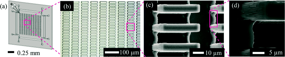 | ||
| Fig. 1 (a) 2D sketch of the microchip with sample inlets (*), microfluidic inlets and outlets, glass pillars and capillary barriers. (b) Optical microscopy image of the glass pillar (rectangle) array, capillary barriers (structures between glass pillars) and air-filled channels (light colored areas). (c) Tilted top view image of the glass capillary barriers between glass pillars under SEM; (d) a closer tilted top view of capillary barriers under SEM. The depth, width, and length of the pillars and capillary barriers are 20 × 4 × 5 μm and 4 × 1 × 3 μm, respectively. | ||
This design was fabricated using two consecutive reactive ion etching (RIE) steps to define glass pillar and capillary barrier height for hydrogel containment. Before each RIE process, an SU-8 layer was spin-coated on the wafer. The SU-8 layer served as a mask during the subsequent dry etching process to fabricate the structures in the underlying wafer. A photolithography step was performed to pattern the structure layout in SU-8. After the postbake step, the exposed layer was developed and dry etched. Subsequently, the SU-8 layer was stripped in a piranha bath. The etch depth of the structures was 15 μm measured after the first RIE step. After the second RIE step, the etch depth was 20 μm for the channels and 15 μm for the capillary barriers. The final capillary barrier structures were uniform, stable and reproducible. Fig. 1c depicts glass pillars, capillary barriers, and channels after the second RIE step. Buffer reservoirs together with fluidic inlets and outlets were opened on the back side of the wafer by powder blasting. To pattern the holes, the wafer was laminated with an Ordyl tape resist (BF410; Tokyo Ohka Kogyo). The foil was then developed using 1% of NaHCO3, powder blasted with Al2O3 particles, and subsequently removed by acetone. Finally, the processed wafer was thermally bonded with a plain fused silica wafer. The minimum feature size obtained by the classical lithography and reactive ion etching processes are emerging as physical limitations on the hydrogel patterning by capillary barriers. This limitation can become an issue in the next-generation microfluidic devices where less than picoliter-volume size hydrogel patterns are needed.
Surface silanization
Silanization allows the hydrogel to covalently bond to the glass surface, increases the mechanical stability of the hydrogel structures in the chip, and decreases the surface wettability of the fused silica.26 The inner walls of the microchip were therefore silanized to enable the formation of covalent bonds between the glass plate and the hydrogel. To achieve this, the microchip was cleaned in 0.1 M NaOH for 30 min in an ultrasonic bath. The microchip was rinsed with DI water and placed in a solution of 2![[thin space (1/6-em)]](https://www.rsc.org/images/entities/char_2009.gif) :3:5 (v/v/v) 3-trimethoxysilyl propyl methacrylate (Sigma):glacial acetic acid (Sigma):DI water for 60 min. After rinsing with DI water and acetone, the microchips were dried at 110 °C to promote covalent siloxane bond formation to the glass surface.25,26 Fig. S1a, ESI,† shows a photopolymerized polyacrylamide hydrogel block firmly adhered to the silanized glass plate.
:3:5 (v/v/v) 3-trimethoxysilyl propyl methacrylate (Sigma):glacial acetic acid (Sigma):DI water for 60 min. After rinsing with DI water and acetone, the microchips were dried at 110 °C to promote covalent siloxane bond formation to the glass surface.25,26 Fig. S1a, ESI,† shows a photopolymerized polyacrylamide hydrogel block firmly adhered to the silanized glass plate.
Hydrogel preparation and patterning
A polyacrylamide hydrogel precursor was prepared by blending 20% acrylamide/bis solution (19:1) (BioRad), 2% 2,2-dimethoxy-2-phenylacetophenone (Invitrogen) and 2% ammonium persulfate (Invitrogen) solutions. A pore size range between 10 and 50 nm was obtained, as shown in the ESI,† Fig. S1b. Preparation, patterning and polymerization of precursor solution were performed under N2 flow due to the oxygen sensitivity of polyacrylamide. Polyethylene glycol diacrylate (PEG DA) (MW, 3400) (Laysan Bio, Inc.) was dissolved in PBS at 15% w/v and combined with 10% 2-hydroxy-1-[4-(2-hydroxyethoxy)phenyl]-2-methyl-1-propane (Irgacure 2959) (Sigma) solution to prepare the PEG DA hydrogel precursor. No special equipment was used in preparation, patterning and polymerization of PEG DA precursor solution. A collagen hydrogel precursor was prepared by blending purified collagen solution (Advanced Biomatrix, Inc.) with 10× PBS, and 1 M NaOH (a collagen:PBS:NaOH ratio of 8:1:1). An agarose hydrogel precursor was prepared by dissolving ultrapure agarose powder (Invitrogen) in 1× TBE buffer at 0.5% w/v in a hot water bath. Preparation and gelation of collagen and agarose precursor solutions were performed under ambient conditions. Patterning of the agarose hydrogel was performed on a hot plate adjusted to 45 °C.
Fig. 2a–f outline the hydrogel fabrication process. Immediately after the silanization (Fig. 2b), the precursor solutions were injected into the closed microchip. The entire void space in the chip was then filled by capillary action owing to the positive pressure applied through pipetting (Fig. 2c). Excess precursor solution was subsequently removed by vacuum suction through the outlets (Fig. 2d). In this stage, the hydrogel precursor remained contained between the pillars due to capillary pinning at the barriers. No air bubbles were trapped in the microchip during filling and emptying. The patterned polyacrylamide and PEG DA hydrogel precursors were then cured by UV light at 400 mW cm−1 for 3 min (Fig. 2e), while the patterned collagen hydrogel precursor was placed in an incubator at 37 °C and the patterned agarose hydrogel precursor was cooled to room temperature for gelation (Fig. 2f). Processed microchips were kept in DI water at room temperature. In this process, ~1.25 pL hydrogel structures with 4 × 20 × 20 μm dimensions were produced for all of the photopolymerized and thermo-gelling hydrogel types, confirming the versatility of the method. The final hydrogel patterns were robust with a patterning consistency of more than 99% as seen in the ESI,† Table S1, Fig. S2 and S3.
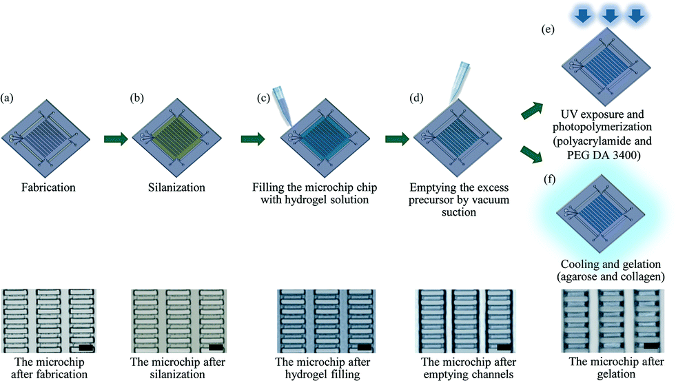 | ||
| Fig. 2 Fabrication process flow for custom hydrogel patterning in a closed microfluidic chip. Scale bars indicate 15 μm for all images. | ||
Contact angles of hydrogels on fused silica surface were measured using the Dataphysics OCA-20 contact angle software. Scanning electron microscopy (SEM) images were taken using a JEOL JSM 5610 field emission scanning electron microscope.
Capillary barrier operating principle
Hydrogel precursor was pinned by the capillary barriers in the channels during vacuum suction. Pinning is attributed to the abrupt expansion in the cross-sectional geometry of the channel at the barriers, hydrogel meniscus alteration and the local Laplace pressure change (Fig. 3a).24 As described in the literature, the Laplace pressure is determined by the angle of expansion and constriction at the abrupt expansion point, channel height, capillary barrier height, and the contact angle, θ, between the channel wall and the hydrogel, requiring 45° < θ < 90° (Fig. 3a).23,27–30 The latter requirement is consistent with our measurements of the contact angle at capillary barriers, which was found to be 62.9° ± 8.4° after silanization. Fig. 3a illustrates the top view of the channel structure and hydrogel pinning during vacuum suction. Hydrogel overflow does not occur at the capillary barriers despite the fact that the hydrogel did not recede with the same speed from neighboring channels during vacuum suction.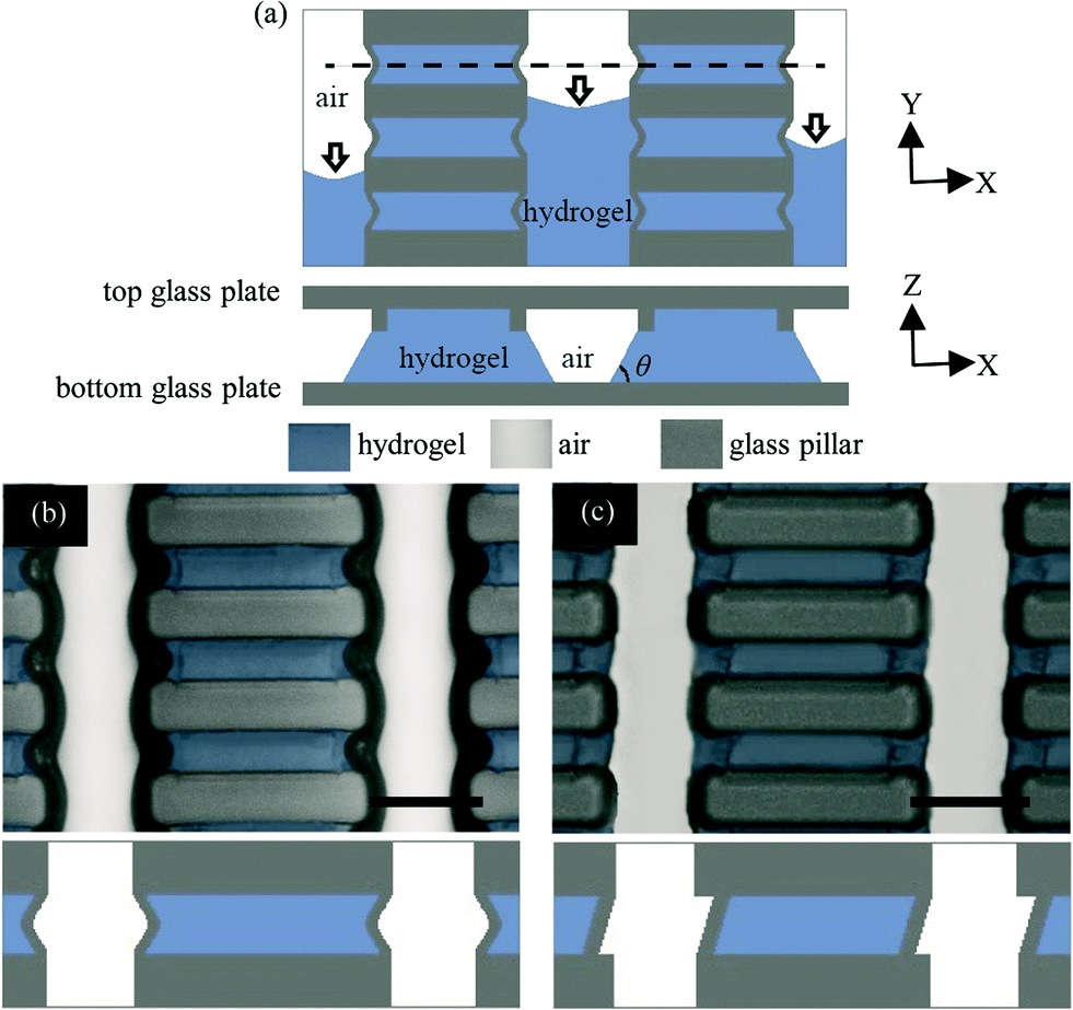 | ||
| Fig. 3 (a) Top and cross-sectional schematic views of meniscus pinning at capillary barriers. Direction of the hydrogel flow in channels during vacuum suction is indicated by arrows and cross-sectional planes are shown by dashed lines. Phase contrast microscopy image of custom patterned polyacrylamide trapped in between glass pillars after photopolymerization using (b) parenthesis-shaped capillary barriers and (c) slash-shaped capillary barriers (the images are artificially colored on the basis of gray scale differences). Scale bars indicate 10 μm for all images. | ||
The pinning performance theoretically improves with the increasing capillary barrier-to-channel height ratio. Barriers with one fourth of the channel height were chosen as optimal in this study.23
We also studied the effect of the capillary barrier shape on hydrogel pinning. Both slash- and parenthesis-shaped capillary barriers were tested for their pinning performance. As depicted in Fig. 3b and c, the barriers in the top view show an acute angle to the pillar walls. A capillary barrier glass pillar wall interface angle of 60° was found to facilitate microchip filling for both parenthesis- and slash-shaped barriers.
The pinning performance of the parenthesis-shaped barrier, slash-shaped barrier and no barrier geometries was evaluated on a passed/failed basis. For this evaluation, three representative images were collected from two opposite corners and the middle part of the arrays. In case of microchips with barriers, full hydrogel occupation between both barriers was counted as passed. In case of microchips without barriers, hydrogel patches covering the entire gap between glass pillars were counted as passed. All other configurations were counted as failed. The pinning performance of the parenthesis-shaped barriers during hydrogel emptying was slightly superior to the slash-shaped ones (P > 0.9). Both parenthesis- and slash-shaped capillary barriers demonstrate statistically significant superiority (P < 0.0001) when compared to the no capillary barrier geometry (ESI,† Fig. S2, Table S1). These findings are in accordance with previous reports, describing that an acute angle at both ends of the barrier provides a minimal meniscus stretching and maximal surface wetting area for the hydrogel precursor.23
Conclusions
In summary, non-fluorescent capillary barriers were used to fabricate high-resolution hydrogel structures over large areas with neither defects nor distortions in closed microchips. Small volumes of different hydrogel types, fabricated with photopolymerization and thermo-gelation, were uniformly patterned using this method. This design strategy allows for robust processing of elaborate microfluidic networks consisting of ~400k periodic picoliter-volume hydrogel patterns. Capillary barrier technology is a highly reliable technique, enabling full control over selective hydrogel patterning and allowing for fluorescence-based analyses. Picoliter volume hydrogel microarray patterning is a promising unique method with great potential for biological and clinical applications, such as subdivided-hydrogel microarrays for bacteria cultures31,32 and 3D cell cultures,33 and enclosed hydrogel microarrays for electrokinetic biomolecule separation purposes.34 Although our demonstration is limited to hydrogel formation, patterning of aqueous solutions would be equally possible, for example enabling massively parallel liquid35 and droplet36 patterning in microfluidic devices, and liquid compartmentalization for sensing and bioassays.37Acknowledgements
This work was funded by the Dutch network for Nanotechnology NanoNext NL in the subprogram “Nanofluidics for Lab-on-a-chip”. The authors thank Wim J. Hendrikson for supplying PEG DA, and Mustafa Akin Sefunc, Allison C.E. Bidulock, Jan van Nieuwkasteele and Paul Vulto for thorough discussions.Notes and references
- G. M. Eichenbaum, P. F. Kiser, S. A. Simon and D. Needham, Macromolecules, 1998, 31, 5084 CrossRef CAS PubMed.
- M. E. Harmon, M. Tang and C. W. Frank, Polymer, 2003, 44, 4547 CrossRef CAS.
- T. Tanaka, I. Nishiq, S. Sun and S. Ueno-Nishio, Science, 1982, 218, 467 CAS.
- A. Suzuki and T. Tanaka, Nature, 1990, 3464, 345 CrossRef.
- B. G. Chung, K. H. Lee, A. Khademhosseini and S. H. Lee, Lab Chip, 2012, 12, 45 RSC.
- M. Lei, A. Baldi, E. Nuxoll, R. A. Siegel and B. Ziaie, Diabetes Technol. Ther., 2006, 1, 112 CrossRef PubMed.
- J. Han and H. G. Craighead, Science, 2000, 5468, 1026 CrossRef.
- S. N. Bhatia and V. A. Liu, Biomed. Microdevices, 2002, 4, 257 CrossRef.
- J. S. Paustian, R. N. Azevedo, S. T. B. Lundin, M. J. Gilkey and T. M. Squires, Phys. Rev. X, 2013, 3, 1 Search PubMed.
- H. D. Jang, S. K. Kim, H. Chang, K. M. Roh, J. W. Choi and J. Huang, Biosens. Bioelectron., 2012, 38, 184 CrossRef CAS PubMed.
- W. G. Koh and M. Pishko, Sens. Actuators, B, 2005, 106, 335 CrossRef CAS PubMed.
- N. Y. Lee, Y. K. Jung and H. G. Park, Biochem. Eng. J., 2006, 29, 103 CrossRef CAS PubMed.
- J. Liu, D. Gao, H. F. Li and J. M. Lin, Lab Chip, 2009, 9, 1301 RSC.
- D. J. Beebe, J. S. Moore, J. M. Bauer, Q. Yu, R. H. Liu, C. Devadoss and B. Jo, Nature, 2000, 404, 588 CrossRef CAS PubMed.
- M. E. Helgeson, S. C. Chapin and P. S. Doyle, Curr. Opin. Colloid Interface Sci., 2011, 16, 106 CrossRef CAS PubMed.
- M. S. Hahn, L. J. Taite, J. J. Moon, M. C. Rowland, K. A. Ruffino and J. L. West, Biomaterials, 2006, 27, 2519 CrossRef CAS PubMed.
- D. Chandra, J. A. Taylor and S. Yang, Soft Matter, 2008, 4, 979 RSC.
- J. Peng, D. Zhao, X. Tang, F. Tong, L. Guan, Y. Wang, M. Zhang and T. Cao, Langmuir, 2013, 29, 11809 CrossRef CAS PubMed.
- G. Eng, B. W. Lee, H. Parsa, C. D. Chin, J. Schneider, G. Linkov, S. K. Sia and G. Vunjak-Novakovic, Proc. Natl. Acad. Sci. U. S. A., 2013, 110, 4551 CrossRef CAS PubMed.
- X. Y. Jiang, J. M. K. Ng, A. D. Stroock, S. K. W. Dertinger and G. M. J. Whitesides, Am. Chem. J., 2003, 125, 5294 CrossRef CAS PubMed.
- S. Podszun, P. Vulto, H. Heinz, S. Hakenberg, C. Hermann, T. Hankemeier and G. A. Urban, Lab Chip, 2012, 12, 451 RSC.
- S. J. Trietsch, G. D. Israëls, J. Joore, T. Hankemeier and P. Vulto, Lab Chip, 2013, 13, 3548 RSC.
- P. Vulto, G. Dame, U. Maier, S. Makohliso, S. Podszun, P. Zahn and G. A. Urban, Lab Chip, 2010, 10, 610 RSC.
- M. Stoneman, M. Fox, C. Zeng and V. Raicu, Lab Chip, 2009, 9, 819 RSC.
- R. N. Lamb and D. N. Furlong, J. Chem. Soc., Faraday Trans., 1982, 78, 61 RSC.
- J. B. Brzoska, I. Ben Azouz and F. Rondelez, Langmuir, 1994, 10, 4367 CrossRef CAS.
- J. Vidič, A. Podgornik and A. Štrancar, J. Chromatogr. A, 2005, 1065, 51 CrossRef PubMed.
- L. J. Yang, T. Yao and Y. C. Tai, J. Micromech. Microeng., 2004, 14, 220 CrossRef.
- P. F. Man, C. H. Mastrangelo, M. A. Burns and D. T. Burke, MEMS’98 Conference Proceeding, 1998, vol. 45 Search PubMed.
- S. Chibbaro, E. Costa, D. I. Dimitrov, F. Diotallevi, A. Milchev, D. Palmieri, G. Pontrelli and S. Succi, Langmuir, 2009, 25, 12653 CrossRef CAS PubMed.
- P. Krsko, J. B. Kaplan and M. Libera, Acta Biomater., 2009, 5, 589 CrossRef CAS PubMed.
- D. Puchberger-Enengl, S. Podszun, H. Heinz, C. Hermann, P. Vulto and G. A. Urban, Biomicrofluidics, 2011, 5, 044111 Search PubMed.
- A. Y. Rubina, A. Kolchinsky, A. A. Makarov and A. S. Zasedatelev, Proteomics, 2008, 8, 817 CrossRef CAS PubMed.
- J. Fu, R. B. Schoch, A. L. Stevens, S. R. Tannenbaum and J. Han, Nat. Nanotechnol., 2007, 2, 121 CrossRef CAS PubMed.
- T. Hossein, A. Jovic, B. Mosadegh, Q. Y. Lee, X. Liu, K. E. Luker, G. D. Luker, S. J. Weiss and S. Takayama, Nat. Mater., 2009, 8, 736 CrossRef PubMed.
- T. Tonooka, K. Sato, T. Osaki, R. Kawano and S. Takeuchi, Small, 2014, 16, 3275 CrossRef PubMed.
- R. R. Pompano, W. Liu, W. Du and R. F. Ismagilov, Annu. Rev. Anal. Chem., 2011, 4, 59 CrossRef CAS PubMed.
Footnote |
| † Electronic supplementary information (ESI) available. See DOI: 10.1039/c4lc01350f |
| This journal is © The Royal Society of Chemistry 2015 |