
 Open Access Article
 This Open Access Article is licensed under a Creative Commons Attribution-Non Commercial 3.0 Unported Licence
A superhydrophobic chip based on SU-8 photoresist pillars suspended on a silicon nitride membrane†
Giovanni
Marinaro
ab,
Angelo
Accardo
b,
Francesco
De Angelis
b,
Thomas
Dane
a,
Britta
Weinhausen
a,
Manfred
Burghammer
ac and
Christian
Riekel
*a
aEuropean Synchrotron Radiation Facility, B.P.220, F-38043 Grenoble Cedex, France. E-mail: riekel@esrf.fr
bIstituto Italiano di Tecnologia, Via Morego 30, Genova 16163, Italy
cDepartment of Analytical Chemistry, Ghent University, Krijgslaan 281, S12B-9000 Ghent, Belgium
First published on 28th July 2014
Abstract
We developed a new generation of superhydrophobic chips optimized for probing ultrasmall sample quantities by X-ray scattering and fluorescence techniques. The chips are based on thin Si3N4 membranes with a tailored pattern of SU-8 photoresist pillars. Indeed, aqueous solution droplets can be evaporated and concentrated at predefined positions using a non-periodic pillar pattern. We demonstrated quantitatively the deposition and aggregation of gold glyconanoparticles from the evaporation of a nanomolar droplet in a small spot by raster X-ray nanofluorescence. Further, raster nanocrystallography of biological objects such as rod-like tobacco mosaic virus nanoparticles reveals crystalline macro-domain formation composed of highly oriented nanorods.
Introduction
The sensitivity for probing low molecular concentrations of molecules or nanoparticles by X-ray scattering techniques can be considerably amplified by evaporating quasi contact-free droplets on superhydrophobic surfaces (SHSs).1 Indeed, assembly processes at the interface of an evaporating droplet or the heterogeneity of its residue can be probed in situ by raster-scan X-ray diffraction (XRD) with μm- or sub-μm step-resolution defined by the focal spot size.1 The absorption of SHSs based on standard silicon wafers of ~500 μm in thickness is, however, ~82% at a λ = 0.1 nm wavelength.2 This poses no problem if the X-ray beam is oriented parallel to the surface when probing a droplet.1 Raster-scan probing of residues in transmission geometry can also often be performed after separating the residue from the substrate.3 This is not possible for fragile residues such as filamentous extensions. Such morphologies are, however, of particular interest for XRD probing due to extensional flow alignment during the pinning transition.1 An alternative is using SHSs based on thin Si-substrates with holes etched between the pillars.4 Although the X-ray absorption of a ~50 μm thick Si-substrate is only ~16%, the correction for variation in absorption due to the presence of holes requires elaborate post-processing software. Our aim was therefore to develop a SHS showing high quasi-homogeneous X-ray transmission and incorporating a periodic as well as non-periodic pillar patterning.5,6 This latter feature can help in keeping the droplet localized during evaporation or predefine the position of a residue speckle for probing by an X-ray beam.6We report here the fabrication of SHS-chips based on a 0.5 μm thick Si3N4 substrate (~99.9% X-ray transmission) and ~12 μm high SU-8 photoresist pillars (~99.8% X-ray transmission) showing also high optical and IR transmission. To explore the solution concentration capability of the chips, we probed a gold glyconanoparticle residue by nanobeam X-ray fluorescence (nanoXRF). As an example of a weakly scattering biomaterial, we studied a tobacco mosaic virus (TMV) residue by nanobeam X-ray diffraction (nanoXRD). The experimental protocol and setup are shown schematically in Fig. 1A and B.
 | ||
| Fig. 1 A: A droplet (about 4 μL) is evaporated on the Si3N4 membrane equipped with superhydrophobic SU-8 micropillars and the solute is concentrated. B: The schematic experimental setup allowing XRD and XRF experiments. The monochromatic beam from an undulator source is focused by refractive lenses7 on a submicron spot on the sample. The residue is raster-scanned through the nanobeam. An XRD pattern and an XRF spectrum (optionally) are recorded at every position. | ||
Materials and methods
Device microfabrication
We fabricated three masks for generating (i) a matrix of Si3N4 membranes, (ii) a periodic hexagonal lattice of 10 μm in diameter SU-8 pillars with a 30 μm pitch8 and (iii) a non-periodic lattice of SU-8 pillars defined by an analytical function with the pillar separation decreasing towards the center of the chip thus inducing a gradient in wettability.5,6 We used a 2 inch <100> oriented silicon wafer with a 0.5 μm Si3N4 layer on both sides. A photolithography step was used to protect the membrane from the following reactive ion etch (RIE) process uncovering the silicon according to the pattern of the 1st mask defining the Si-frames of the membranes of the individual chips. The silicon was removed by wet etching with KOH solution. A layer of SU-8 photoresist was then spin-coated on the wafer and structured by a 2nd photolithography process on the other side of the chip which involved an alignment step to match the pattern of the frames on the opposite side. The pillars and the Si3N4 membrane were covered with a ~20 nm thick Teflon (C4F8) layer by plasma deposition (ESI†).The SHS-chips were characterized by optical microscopy and scanning electron microscopy (SEM) (Fig. 2A, B and 3A, B). We measured a contact angle for a 4 μL water droplet of Θ = 151.2° on a periodic pillar SHS-chip (ESI†).
 | ||
| Fig. 2 A: A scanning electron microscopy (SEM) image of the central part of a non-periodic SU-8 pillar lattice on the Si3N4 substrate. B: A single SU-8 pillar of ~12 μm in height. The pillars and substrate are covered with a ~20 nm layer of Teflon. | ||
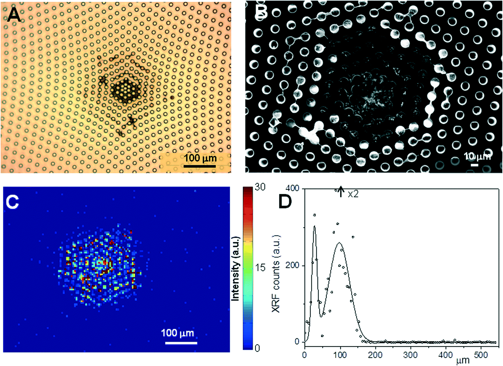 | ||
| Fig. 3 A: An optical image of gold nanoparticles deposited on a non-periodic pillar SHS-chip. B: A SEM image of the inner part of SHS showing pillars interconnected by filaments. C: C-XRF corresponding to a step-resolution of 5 μm based on the Au Lα band. D: A radial XRF profile obtained by azimuthally integrating the C-XRF. Two Gaussian profiles have been fitted as guides to the eye. The center (0 μm) is defined at the highest pillar density (Fig. 2A). | ||
Materials
Colloidal gold nanoparticles (AuNPs) with ligand-functionalized surfaces provide elements for bottom-up assembly of functional nanostructures which are of interest for mimicking biological systems.9 We deposited a ~4 μL droplet of 5 nM gold glyconanoparticles in deionized water on the SHS-chip (Fig. 1A). The ~2.9 nm diameter particles consist of a 1.3 ± 0.3 nm diameter core corresponding on average to 71 gold atoms and were functionalized with a ~0.8 nm carbohydrate shell.10 We will use below the abbreviation Au71NP (ESI†).TMV is a plant-virus that forms filamentous structures.11 The TMV particles have a rod-like shape of ~300 nm in length and ~18 nm in diameter.12 We used a solution of 405 mg ml−1 TMV particles in 1 mM EDTA solution + 0.1% azide, pH 7.2. The solution was diluted by a factor of 100 with deionized water. The deposited droplet volume was set also to ~4 μL.
The SU-8 25 photoresist was obtained from MicroChem.
Synchrotron radiation experiments
A λ = 0.08321 nm monochromatic X-ray beam was focused on a ~170(h) × 130(v) nm2 spot by Si refractive lenses7 with a flux of ~2 × 10⁹ photons s−1 at the sample position. Experiments were performed in transmission geometry with the beam normal to the substrate (Fig. 1B). XRF spectra were recorded in the horizontal scattering plane using a Si-drift detector. XRD data were collected using a CCD camera with an X-ray converter screen and 2K × 2K pixels of 50 × 50 μm2 each. The sample was step-scanned through the beam using an x/y/z piezo stage (ESI†). Background scattering from the substrate was very small and did not contribute discrete peaks or short-range order to the XRD patterns.Results and discussion
NanoXRF probing of gold nanoparticles
Optical and SEM images of the Au71NP residue on the non-periodic SHS-chip are shown in Fig. 3A and B. The composite XRF image (C-XRF) is composed of “pixels” scaled to the local integrated Au Lα band (Fig. 3C). The azimuthally integrated XRF profile is shown in Fig. 3D. Two Gaussian profiles were fitted to the XRF profile suggesting two deposition zones around the chip center (Fig. 3D). The residue deposited close to the center of the gradient pattern extends radially to ~50 μm. This is surrounded by a broader residue distribution extending radially to ~150 μm. We attribute this to nanoparticles deposited at the contact line during the pinning transition. Although a number of pillars are connected by filaments (Fig. 3B), the nanoparticle concentration was not high enough to form a continuous coffee-ring type13 residue. The XRF profile shows complete confinement of the nanoparticles within the two zones. We note that for ultralow concentrations of organic and biological matter, the residue is only deposited in the central zone.5Nanodiffraction probing of TMV nanorods
The optical image of a part of the TMV residue deposited on a periodic, pillared SHS-chip shows the formation of a coffee-ring type residue13 on the pillars (Fig. 4A). A composite XRD (C-XRD) image14 based on a raster scan with 0.5 μm steps is shown in Fig. 4B. Each “pixel” corresponds to a single diffraction pattern as the one shown in Fig. 4C. The observed reflections agree with the hexagonal TMV lattice with the nanorods oriented along the c-axis.15 A helical pitch of 2.202(5) nm derived from the n = 3 layer-line reflections confirms the small pitch reduction for dried TMV residues15 as compared to TMV sols.16 | ||
| Fig. 4 A: An optical image of the TMV residue on periodic pillared SHS-chip. B: A C-XRD image based on an 81 × 81 “pixel” mesh scan with a 0.5 μm step size. C: A single XRD pattern from the outer-rim interface. The positions of the equator (n = 0) and n = 3/−3 layer lines are indicated. The c-axis direction (arrow) corresponds also to the direction of the long axis of the schematically depicted TMV nanorod.15 D: A C-XRD image of the dashed square in (B) with a schematic interface line. The upper display range is limited to the n = 3/−3 layer lines although scattering from the n = 6/−6 layers is also observed. The orientation of the local c-axis, corresponding to the TMV nanorod-axis, is indicated by an arrow. | ||
The limitation of the display range to the strongest low-order reflections on the n = 0 layer-line (Fig. 4C) implies that Ewald’s sphere17 is large with respect to interatomic distances and the reflection conditions are fulfilled for all patterns. Given a quasi-constant microstructure across the scanned area, the C-XRD image reflects in first order the mass density modulations projected on a plane normal to the beam direction.14
The C-XRD image reveals increased deposition around the inner-rim pillar as well as a narrow transition zone between the outer-rim pillar and the outer rim interface (Fig. 4B). There is also increased deposition in the area connecting the inner-rim and outer-rim pillars. We even observe in the optical and C-XRD images a thin residue layer on the outer-rim pillar which is the remnant of the retreating triple contact-line (Fig. 4A, B).
A more detailed microstructural analysis of the local nanorod orientation provides information on the arrested flow pattern of the nanorods. Indeed, we noted the formation of a macrodomain at the outer rim with the nanorod axes aligned parallel to the interface (Fig. 4D). Such an orientation has also been observed for the rim of a TMV coffee-ring on a glass substrate and attributed to capillary effects.15 A more detailed analysis of the arrested nanorod flow pattern is beyond the scope of the present note.
Conclusions
SHS-chips based on a thin Si3N4 membrane with periodic and non-periodic SU-8 photoresist pillar patterns have been fabricated and tested by nanobeam XRF and XRD. Well defined compaction of gold nanoparticles was obtained in the center of a non-periodic pillar pattern. The Si3N4 membrane and the SU-8 pillars show very high X-ray transmission and low background scattering. Weak diffraction signals from highly oriented TMV nanorods at the residue interface could be observed without background correction. Macrodomain formation by flow alignment could be explored for other large anisotropic biological objects in order to induce long-range order.Acknowledgements
We wish to thank F. Gentile (IIT-Genova) and E. Di Fabrizio (KAUST) for very helpful suggestions in the context of the current work. We also thank J. L. Pellequer (CEA Marcoule (IBEB, Service de Biochimie et Toxicologie Nucléaire, Bagnols sur Cèze, France)) for the gift of the TMV particle solution and M. Reynolds (ESRF) for the gold nanoparticle solution. I. Snigireva (ESRF Imaging Laboratory) collected the gold nanoparticle residue SEM image. All other SEM images were recorded at IIT-Genova.Notes and references
- A. Accardo, E. Di Fabrizio, T. Limongi, G. Marinaro and C. Riekel, J. Synchrotron Radiat., 2014, 21, 643–653 CrossRef CAS PubMed.
- B. L. Henke, E. M. Gullikson and J. C. Davis, At. Data Nucl. Data Tables, 1993, 54, 181–342 CrossRef CAS.
- A. Accardo, M. Burghammer, E. D. Cola, M. Reynolds, E. Di Fabrizio and C. Riekel, Langmuir, 2011, 27, 8216–8222 CrossRef CAS PubMed.
- F. Gentile, G. Das, M. L. Coluccio, F. Mecarini, A. Accardo, L. Tirinato, R. Tallerico, G. Cojoc, C. Liberale, P. Candeloro, P. Decuzzi, F. De Angelis and E. Di Fabrizio, Microelectron. Eng., 2010, 87, 798–801 CrossRef CAS PubMed.
- F. Gentile, M. L. Coluccio, E. Rondanina, S. Santoriello, D. Di Mascolo, A. Accardo, M. Francardi, F. De Angelis, P. Candeloro and E. Di Fabrizio, Microelectron. Eng., 2013, 111, 272–276 CrossRef CAS PubMed.
- E. Miele, M. Malerba, M. Dipalo, E. Rondanina, A. Toma and F. De Angelis, Adv. Mater., 2014, 24, 4179–4183 CrossRef PubMed.
- C. G. Schroer, R. Boye, J. M. Feldkamp, J. Patommel, A. Schropp, A. Schwab, S. Stephan, M. Burghammer, S. Schoeder and C. Riekel, Phys. Rev. Lett., 2008, 101, 090801 CrossRef CAS.
- F. De Angelis, F. Gentile, F. Mecarini, G. Das, M. Moretti, P. Candeloro, M. L. Coluccio, G. Cojoc, A. Accardo, C. Liberale, R. P. Zaccaria, G. Perozziello, L. Tirinato, A. Toma, G. Cuda, E. Cingolani and E. Di Fabrizio, Nat. Photonics, 2011, 5, 683–688 CrossRef.
- B. Pelaz, S. Jaber, D. J. de Aberasturi, W. Wulf, T. Aida, J. M. de la Fuente, H. E. Gaub, L. Josephson, C. R. Kagan, N. A. Kotov, L. M. Liz-Marzán, H. Mattoussi, P. Mulvaney, C. B. Murray, A. L. Rogach, P. S. Weiss, I. Willner and W. J. Parak, ACS Nano, 2012, 6, 8468–8483 CrossRef CAS PubMed.
- M. Reynolds, M. Marradi, A. Imberty, S. Penades and S. Perez, Chem. – Eur. J., 2012, 18, 4264–4273 CrossRef CAS PubMed.
- A. Kendall, M. McDonald, W. Bian, T. Bowles, S. C. Baumgarten, J. Shi, P. L. Stewart, E. Bullitt, D. Gore, T. C. Irving, W. M. Havens, S. A. Ghabrial, J. S. Wall and G. Stubbs, J. Virol., 2008, 82, 9546–9554 CrossRef CAS PubMed.
- A. Klug, Philos. Trans. R. Soc., B, 1999, 354, 531–535 CrossRef CAS PubMed.
- R. D. Deegan, O. Bakajin, T. F. Dupont, G. Huber, S. R. Nagel and T. A. Witten, Nature, 1997, 389, 827–829 CrossRef CAS PubMed.
- C. Riekel, M. Burghammer, R. Davies, R. Gebhardt and D. Popov, in Applications of Synchrotron Light to Non-Crystalline Diffraction in Materials and Life Sciences, ed. M. García-Gutiérrez, A. Nogales, M. Gómez and T. A. Ezquerra, Springer, Heidelberg, 2008 Search PubMed.
- R. Gebhardt, J. M. Teulon, J. M. Pellequer, M. Burghammer, J. P. Colletier and C. Riekel, Soft Matter, 2014, 10, 5458–5462 RSC.
- A. Kendall, M. McDonald and G. Stubbs, Virology, 2007, 369, 226–227 CrossRef CAS PubMed.
- Fundamentals of Crystallography, ed. G. Giacovazzo, Oxford University Press, New York, 1992 Search PubMed.
Footnote |
| † Electronic supplementary information (ESI) available. See DOI: 10.1039/c4lc00750f |
| This journal is © The Royal Society of Chemistry 2014 |