 Open Access Article
 This Open Access Article is licensed under a
 Creative Commons Attribution 3.0 Unported Licence
From chip-in-a-lab to lab-on-a-chip: towards a single handheld electronic system for multiple application-specific lab-on-a-chip (ASLOC)
P.
Neužil
*abc,
C. D. M.
Campos
ad,
C. C.
Wong
c,
J. B. W.
Soon
c,
J.
Reboud†
c and
A.
Manz
a
aKIST Europe Forschungsgesellschaft mbH, Campus E7 1, DE-66 123 Saarbrücken, Germany. E-mail: pavel.neuzil@gmail.com
bCentral European Institute of Technology, Brno University of Technology, Technická 3058/10, CZ-616 00 Brno, Czech Republic
cInstitute of Microelectronics, Singapore Science Park II, 11 Science Park Road, 117685 Singapore
dInstituto de Química, Universidade Estadual de Campinas, Caixa Postal 6154, Campinas, SP CEP 13083-97, Brazil
First published on 25th March 2014
Abstract
We present a portable, battery-operated and application-specific lab-on-a-chip (ASLOC) system that can be easily configured for a wide range of lab-on-a-chip applications. It is based on multiplexed electrical current detection that serves as the sensing system. We demonstrate different configurations to perform most detection schemes currently in use in LOC systems, including some of the most advanced such as nanowire-based biosensing, surface plasmon resonance sensing, electrochemical detection and real-time PCR. The complete system is controlled by a single chip and the collected information is stored in situ, with the option of transferring the data to an external display by using a USB interface. In addition to providing a framework for truly portable real-life developments of LOC systems, we envisage that this system will have a significant impact on education, especially since it can easily demonstrate the benefits of integrated microanalytical systems.
Introduction
The first modern microfluidics devices1 were introduced more than 20 years ago, starting an entirely new field known interchangeably as either micro total analysis systems (μTAS) or lab-on-a-chip (LOC). Even though the devices were made by micromachining and their total area was typically between a few square millimeters to centimeters, they required bulky supporting instrumentation such as pumps and water-cooled Argonne lasers for fluorescence excitation and controls; thus, they could also be called chips-in-a-lab. With the advent of modern technology, electronics and light emitting diodes (LED) among many others, these devices are getting smaller and smaller. The area of LOC has continued to grow extensively, as reflected in the number of commercial products and in the rapidly growing number of published scientific papers.2A large area within microfluidics is dedicated to molecular diagnostics. There are several reviews studying different aspects of LOC development2–4 as well as specific applications,5–8 which predict a burgeoning fate to the field. One of the major requirements for LOC devices to be able to make a significant impact on diagnostics is their portability. This would open another area of applications in point-of-care diagnostics (POC), as so far only dip-stick assays have managed to make a commercial impact, due to the challenging cost limitations of the field. Numerous attempts to develop portable instruments have been presented.9–16 They are typically restricted to a single diagnostic method, such as PCR or LAMP,17 and process either a single analyte or a complex sample.
Here we show a versatile LOC system (Fig. 1) that is completely portable and battery-operated, with the unique advantage of enabling different sensing modalities on a single platform.
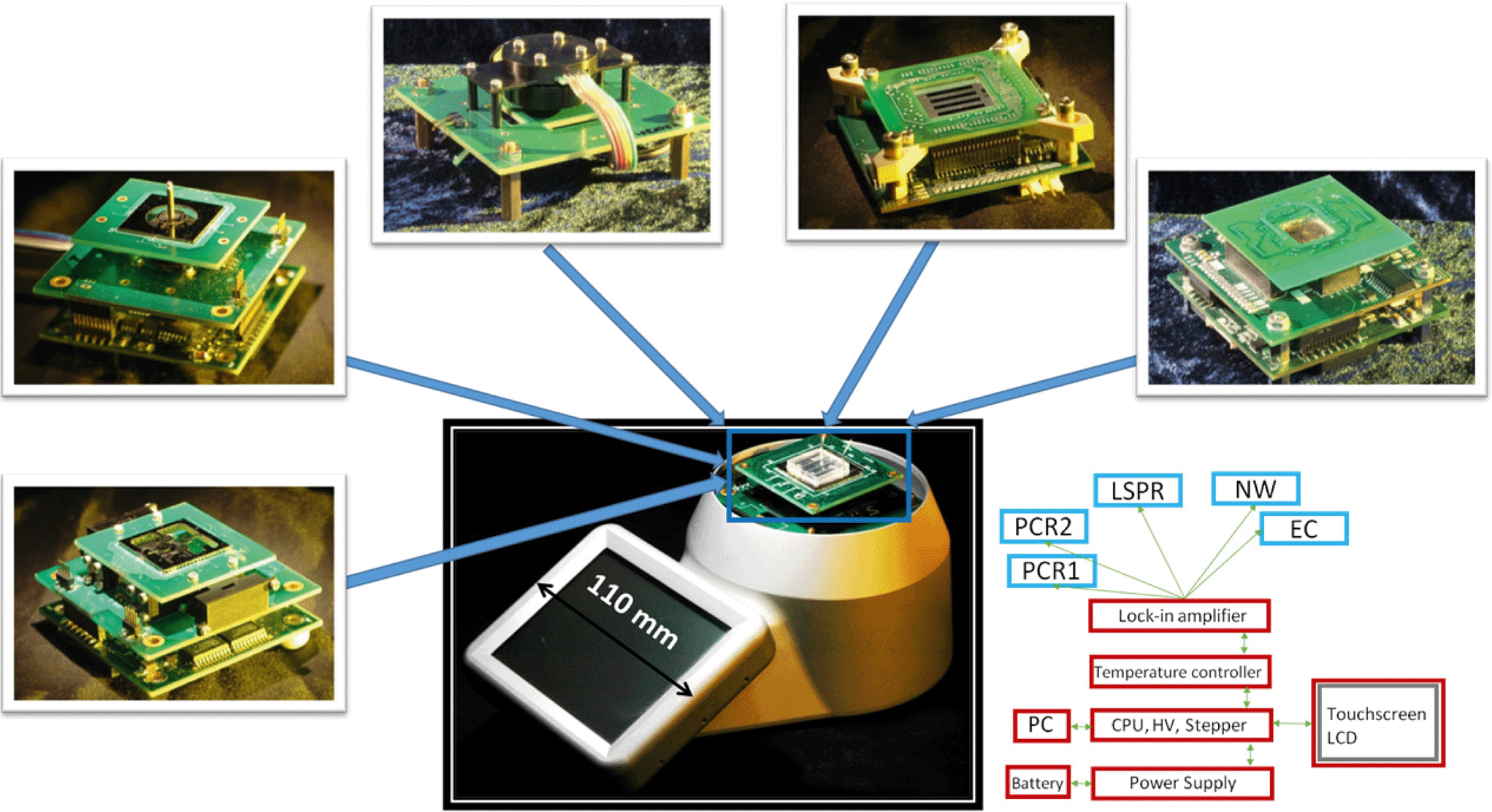 | ||
| Fig. 1 Schematic of the handheld, battery-operated application specific lab-on-a-chip (ASLOC) system. The entire system is placed inside a machined aluminum housing, here showing a nanowire sensing application top chip. It consists of a stack of 4 printed circuit boards to perform functions common to all platforms. Starting from the bottom: the power management board; a board that contains the central processor unit, the high voltage power supply, the stepper motor and touch screen display controller, the USB communication and flash card memory; a board with four independent temperature controllers; a board with four lock-in amplifiers. Other boards are plugged in on-demand to easily configure the LOC to a particular application. Shown clockwise: time domain real-time PCR, space domain real-time PCR (optical parts were removed to show the internals), a localized surface plasmon resonance (LSPR) system, an array of 64 nanowire biosensors and an array of 36 electrochemical sensors. | ||
As the field of microfluidics grows and its applications emerge in the commercial arena, it is essential to introduce its fundamentals and capabilities to the general public, students in particular. Interestingly, the economics and requirements for an educational application are similar to that for POC systems.18 For example, teaching labs conducting molecular biology or analytical chemistry classes19 usually offer students a variety of different techniques, generally based on separate equipments that are only used during a short time each year. This is economically demanding as the tools and equipment are costly. Therefore, testament to the inventiveness of educators, innovative use of common materials has enabled the few first forays into the teaching labs,20 while more complex strategies have been used to demonstrate specialized techniques.21 The introduction of new methods to the teaching lab is usually delayed due to the high costs and expertise required, which has strongly limited the number of universities that feature LOC experiments in their undergraduate teaching courses.
The portable system described here suits such an educational demand. It is based on the natural expansion of a previously developed system for a POC real-time polymerase chain reaction (PCR) diagnostics platform.22–27 The platform is built on a common body which contains a set of controlled voltage sources, a multichannel low-current detection system, a multichannel temperature control system, a regulated high voltage power supply, a stepper motor controller, a display unit and recording media and is powered by a Li-ion battery that can be replaced by a 12 V power supply when suitable. The battery is recharged through a USB interface that is also used to transfer measurement data. It can be customized by selecting a top module matching specific applications from the wide range we have developed, which cover most detection schemes that are utilized in current LOC applications. Application-specific integrated circuits (ASIC) are customized for a specific use. In this context, our system can be called an application-specific LOC (or ASLOC). These applications include real-time PCR in time domain, real-time PCR in space domain, localized surface plasmon resonance (LSPR), impedance measurement of multiple nanowire-based biosensors, and multiplexed electrochemical measurements.
One of the main advantages of the system's design is its ease-of-use. In particular, it is the simplicity of changing application modules, which can be performed with minimal training. As indicated, the specific function of the system is customized by plugging in the required top block, consisting of a stack of up to three PCBs. The operator unscrews four screws, removes the unwanted stack that is plugged in, replaces it with the correct one and tightens the screws back. The software corresponding to the stack is then uploaded into the main system processor (CPU) via a USB interface. We are currently developing a new generation where the user interface is further simplified by having the main processor automatically identifying the boards loaded on the data bus and adjusting its functions accordingly.
Although some of the results of the current work were described in previous studies (see Table 1 for more details), as discussed in the next sections, we include them here to demonstrate the versatility of the platform while focusing on the newly designed systems for NW and electrochemical sensing.
| Module | Ref. | Previous results | Innovations in this work | Microfluidics |
|---|---|---|---|---|
| Time domain PCR | 22,23,25,27 | Demonstration of basic micromachined PCR with external22,23 and internal27 fluorescent detection systems, also integrated with sample preparation.25 | System integration | Virtual reaction chamber (VRC) |
| Space domain PCR | 26 | Demonstrated RT-PCR with sample preparation. Optical detection performed via a separate microscope/camera set-up. The magnet was external to the system. | System integration | VRC |
| LSPR | 28 | The module enabled LSPR measurement in an integrated fashion. The device was cumbersome, resulting in limited portability. | Enhancement by a low profile optical head to reduce the device size. | Covered with microscope slip and fluid dispensed by pipette. |
| Nanowires (NW) | 29 | 4 NW sensors were demonstrated. | System integration for 64 NWs | 64 NW sensors with PDMS channels |
| Electrochemical sensors | N.A. | First description of the system | 64 CE sensors with PDMS channels (being developed) | |
| Temperature sensing | 22 | The system included only a single channel. | Detail description of the sensing with 4 channels | N.A. |
| High voltage controller | N.A. | First description of the system | N.A. |
The range of ASLOC that is shown could be easily augmented with new functionalities by designing new boards at the top (e.g. for photonic and acoustics).
These could also include different microfluidic structures for biological sample manipulation and its delivery to different sensing areas while maintaining portability of the ASLOC and translating microfluidics to the field.
Experimental
Platform development
We describe the main features of the handheld platform adaptable to multiple applications (Fig. 1). It fulfills the requirements for a simple portable LOC system and represents a valuable tool for educational and research laboratories. We designed the system with a clear view to modularity and implemented it in a stack of PCBs, where the core components are located at the bottom while the more specialized parts are at the top. Different applications can be implemented by interchanging the top parts of the system, as will be described in more detail in the next paragraphs.The sensing elements (optical or electrical) presented here are biased by a signal modulated at a suitable frequency, f0, typically around 1 kHz, and synchronously demodulated at its output. The resulting signal is a mixture of a DC component and higher harmonics. These higher harmonics originate from Fourier transforms of interrogating and detecting signals, and they have to be subsequently removed by a low pass filter with a cut-off frequency, f1. The entire system behaves like a band-pass filter “locked” onto the modulating frequency f0, i.e. only signals within the bandwidth from f0 − f1 to f0 + f1 pass the system and can be recorded.
A simple lock-in amplifier was designed from an AD630 integrated circuit (IC) made by Analog Devices, Inc. with the support of a few generic devices such as operational amplifiers, resistors and capacitors. Recently, a miniaturized single channel lock-in fluorescent system was demonstrated,24 but for many applications, such as real-life diagnostics, where controls are required, a single channel is not sufficient. Here we have expanded the system to four channels, which accounts for the majority of currently developed diagnostic targets, such as infectious diseases.30 The requirement to limit the cross talk between the channels, to attain specificity, is achieved by imposing stringent constraints on the modulating frequency f0. All frequencies have to be selected to avoid the matching of higher harmonics up to at least 8th as per our system performance calculation using Fourier transforms. The schematic diagram of the four-channel lock-in amplifier is shown in Fig. 2.
 | ||
| Fig. 2 Diagram of a four-channel lock-in amplifier. (a) The core of the system, consisting of four pulse voltage generators and voltage to current converters (Q1–Q4 BJTs) generating controlled current pulses in four channels for the subsequent block (b or c). The composite current from the block is demodulated by an AD630, followed by a low pass filter. (b) Current powered optical block with 4 LEDs and current to voltage converter. (c) Voltage biased block for electrochemical or impedance measurement with virtual ground and current to voltage converter. | ||
It consists of four voltage pulse generators, each running at its own unique frequency. The voltage pulses are converted into a current by the bipolar junction transistors (BJTs) Q1–Q4 with amplitude set by the emitter resistors R1–R4. The pulsed current signal is fed into another block that can be either directly used to power a set of LEDs or lasers or to run current-to-voltage converters used for electrical measurements, such as electrochemical cells or nanowire sensors. The current to be detected, originating either from a photodiode or from a set of electrochemical sensors or nanowires, is then converted into voltage by a transconductance amplifier. The DC component is separated by capacitive coupling, amplified again and individually demodulated. The signals are then filtered by a low pass filter of the 4th order.
The major part of the four-channel lock-in amplifier (Fig. 2a) is the core of the LOC system described in this paper. It is placed on a single printed circuit board (PCB). The actual function of the system is then determined by another PCB stacked on the lock-in amplifier PCB. Here, we demonstrate two essential systems for optical (Fig. 2b) and electrical measurements (Fig. 2c). Taken together, they cover a large range of the LOC applications currently in use. The overall power consumption of the system of only 4 W makes it a suitable candidate for POC diagnostics as well as for field operations, where the portability and power consumption play an important role. A conventional laptop battery with 1.8 A h capacity can power this LOC for nine hours.
Current-based interrogation
Optical measurement
Our original optical measurement system was only capable of carrying a fluorescence measurement in reflection mode at one spot for real-time PCR.24 However, as stated, this strictly limits the applicability of the system and, in view of an educational application, does not provide the necessary biological positive and negative controls. Here, we have expanded the system to four channels.These have been implemented into two fundamentally different systems, for time domain and space domain measurements. Whilst in both cases the optical signal was processed by an identical electrical circuit, the systems primarily differed in their mechanical construction, and in the path of the optical signal, as described below.
The electrical current pulses generated by the core of the lock-in amplifier CH1–CH4 are directly connected to four LEDs illuminating the sample. The light, either reflected off the sample or generated by the sample itself, interacts with the photodetector and its photocurrent is converted into a voltage and demodulated. The LED can illuminate the sample directly or via a filter. The detection can be performed in reflection, transmission or scattering mode.
Time domain PCR
Fig. 3 shows the implementation of the time domain PCR system. The optics, electronics and silicon micromachined chip were as previously described.27 The PCR was conducted by varying the heaters' temperatures. The fluorescence was simultaneously recorded in a real-time set-up, where an increase in fluorescence intensity is linked to positive amplification.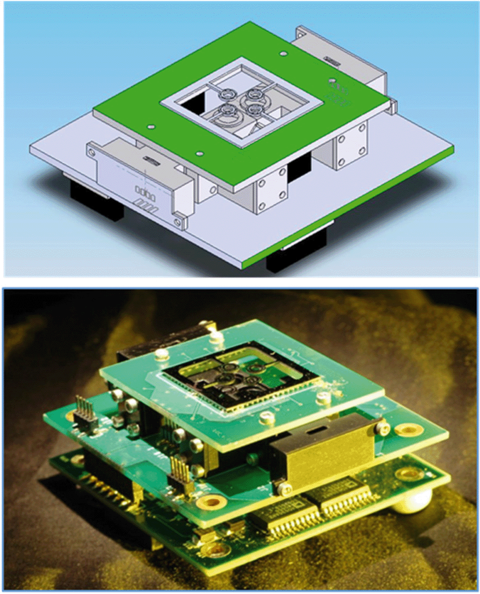 | ||
| Fig. 3 (Top) CAD drawing and (bottom) photograph of a time domain real-time PCR subunit, where the sample is stationary and the temperature cycled by changing the heaters' temperature. | ||
Space domain PCR
Here, a sample containing paramagnetic particles was moved by a magnet placed below the silicon chip on top of the system, while heaters were set at different but constant temperatures. Moving the sample from heater to heater thus resulted in the temperature cycling required for PCR (see Fig. 4). Contrary to our previously published designs,25,26 the magnet is integrated into the handheld instrument, significantly increasing the ease-of-use. The magnet was placed on a circular platform and enabled the rotational motion below the silicon chip. As there was no space for the optical system below, it was placed above the silicon chip as shown in Fig. 4 (top).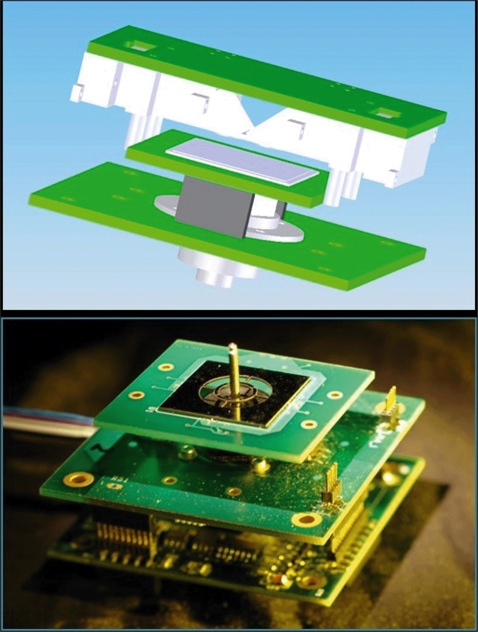 | ||
| Fig. 4 (Top) CAD drawing and (bottom) photograph of a space domain real-time PCR subunit. The CAD design contains the optical housing for fluorescence measurement from the top side, as the bottom is already occupied by a magnet used to move the sample from heater to heater to perform the PCR. | ||
Reflection/absorption measurement – LSPR
In this paper, the LSPR system has been enhanced by a low profile optical head (Fig. 1) to reduce the device size. A scanning electron microscopy (SEM) image of a chip used for localized surface plasmon resonance measurements, the LSPR head as well as the results are shown in Fig. 5.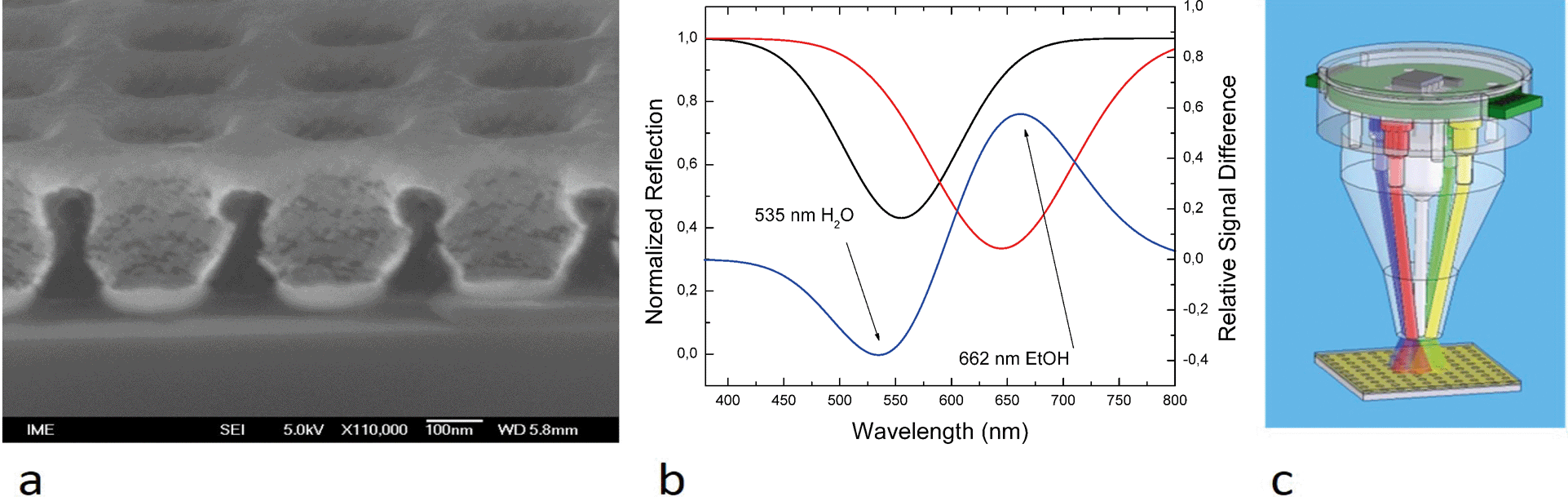 | ||
| Fig. 5 (a) A scanning electron microscopy image of the substrate for measuring surface plasmon resonance. (b) Left axis: normalized amplitude of reflected light from the LSPR chip covered with H2O (black) or ethanol (red). Right axis: the blue line shows the difference between both curves. (c) CAD design of the LSPR head. | ||
Once the chip was covered with water (dispensed manually), the peak of light absorption was at 535 nm as measured by the USB 2000 spectrum analyzer (Ocean Optics, Inc.). When the water was replaced with ethanol, the peak shifted to 662 nm. Using monochromatic illumination at selected wavelengths of 535 nm and 662 nm, the refractive index change was identified. The amplitude of the reflected light will increase at 535 nm during the transition from water to ethanol and simultaneously decrease at 662 nm. Two LEDs with suitable wavelengths can then replace the spectrometer.
We have used the system in optical measurement mode (Fig. 5b–c). The signal generators' outputs were connected to four LEDs with four different colors (wavelengths), and the composite signal was detected by a single photodiode, which was then demultiplexed by four AD630 ICs. This setup is capable of detecting the reflection from the surface of the LSPR chip at four different wavelengths simultaneously.
Voltage-based interrogation
Nanowire-based sensors
Nanowire sensors have received much attention recently due to their attractive surface-to-volume ratio, which promises significant shifts in analytical performance towards ultra-sensitive devices. In a systems perspective, NW can be considered as resistors, the resistance of which varies with external factors such as bending31 or the presence of biomolecules.32 The challenge in their interrogation lies within the small currents available.Here, we modified the blocks described above for electrical current measurement by adding a current-to-voltage converter and thus interrogated the device of interest by voltage. We created a whole family of systems to measure 4 NWs, 64 NWs, and 160 NWs. A CAD design of a 64 NW sensor is shown in Fig. 6. The high number of multiplexing can be a challenge in ASIC solutions,33 and we show here that the handheld system can be used to address array-based applications, such as pathogen typing (e.g. influenza).
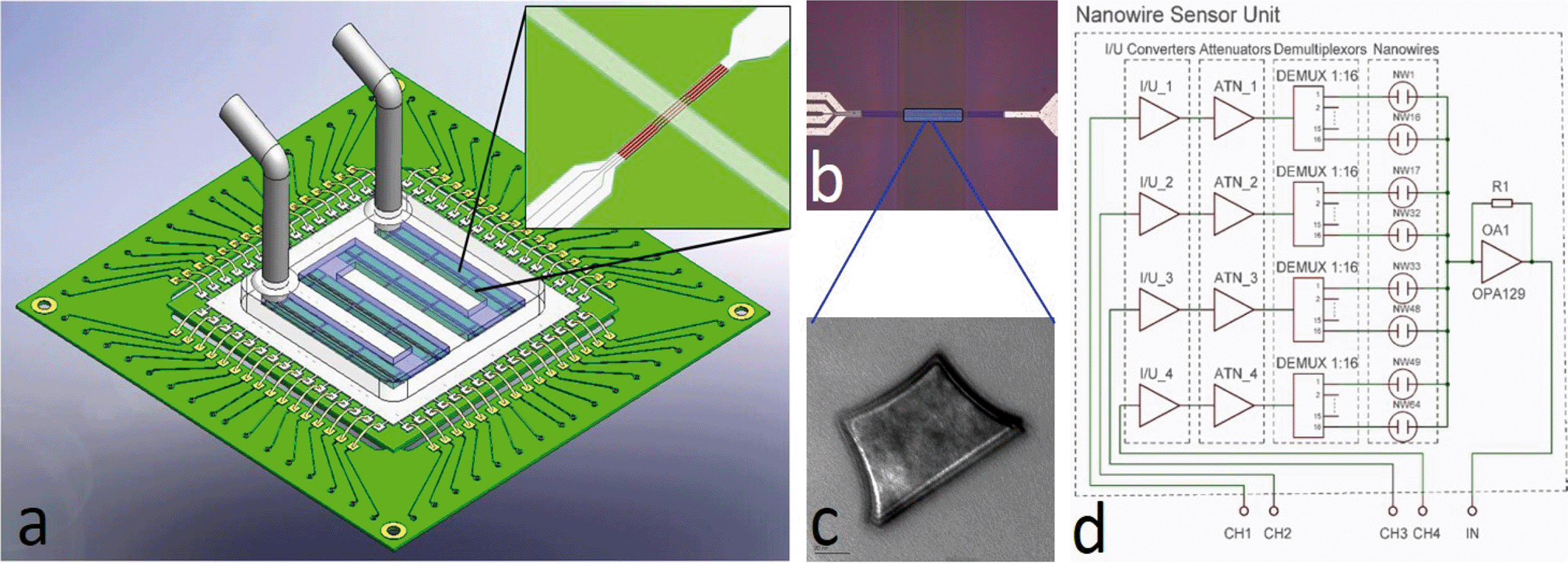 | ||
| Fig. 6 (a) CAD design of the 64 NW sensor with microfluidics channel. The inset shows the microchannel crossing over the nanowire array. (b) A microscope photograph of fabricated 4 NW sensors. (c) A TEM image of a NW cross section. Inset scale bar is 20 nm long. (d) A circuit diagram of voltage-based interrogation with an option to measure 64 NW sensors. | ||
The NW measurement is based on generating voltage pulses by four signal generators controlled by a single chip controller at selected frequencies. The voltage pulses are converted into a current by a bipolar junction transistor (BJT) with the maximum current set by resistors R1–R4. The pulses are converted into voltage by I/V converters, attenuated to 200 mV by ATN1_1–ATN_4 (Fig. 6d), and connected to the first terminal of each NW sensor. The second terminal of all nanowires is common and connected to the trans-impedance amplifier with a high value resistor in a feedback loop. The amplifier output is connected via capacitive coupling to a second amplifier (OA2) with gain set to 100×. The amplified voltage output is fed into a set of demultiplexers together with the original pulses from the signal generators. Only the coherent fraction of the inputs passes the filter. The AC component is filtered out by a low pass filter of the 4th order.
The system has a gain of:
 | (1) |
Electrochemical sensors
The principle of electrochemical sensing is very similar to the NW measurement, with the added requirement of a DC bias for reference/counterelectrode. We added a sawtooth signal into the circuit at the nodes between current-to-voltage (I/U) converters and attenuators (ATNs) in Fig. 6d.Each sensing unit has a working electrode and a combined reference/counterelectrode. The use of combined electrodes, as well as its working principle, was described earlier.35 In this paper, we present a design containing 36 (see Fig. 7) or 64 blocks of four sensing units connected to a common ground. The sawtooth signal was generated using a signal generator 33120A (Agilent GmbH), while the system has the capability of programming an internal voltage generator to perform cyclic voltammetry autonomously. This signal was used in the lock-in amplifier to bias one of the reference electrodes. The resulting signal was then passed through four analog multiplexers 1 × 16. An application for a personal computer was developed to either select a single unit (of 4 sensors) or scan the entire chip (9 or 16 units) with a pre-defined time per unit. The output voltage from the lock-in amplifier can be correlated with the sawtooth signal to extract a differential scanning voltammogram. The communication between the signal generator and the board was conducted via an RS232 interface.
 | ||
| Fig. 7 A photograph of a 36-cell electrochemical chip. | ||
All working electrodes were connected. The common node was connected to a current/voltage converter via a virtual ground. The converted output voltage was consequently proportional to the sum of currents flowing into all working electrodes. This composite current was then processed by demodulators and split into four individual channels. The amplitude of the DC signal in each channel corresponded to the current in the respective electrochemical cell.
Results and discussion
Nanowire-based sensing system
Fig. 8 shows the system setup for biosensing applications. The NW chip contained 64 sensors clustered into 16 groups, each containing 4 individual NW sensors. The chip was connected electrically and mechanically to the PCB by using a bespoke soldering tool. It consisted of a PCB holder, a pneumatically actuated heated soldering head and a timer. The PCB was placed underneath the head, which was heated up to a temperature of ca. 240 °C and its motion was activated. It then went down, pressed the chip against the PCB for 2 s and moved back into its original position. During those 2 s, the silicon chip was heated up and soldered onto the PCB.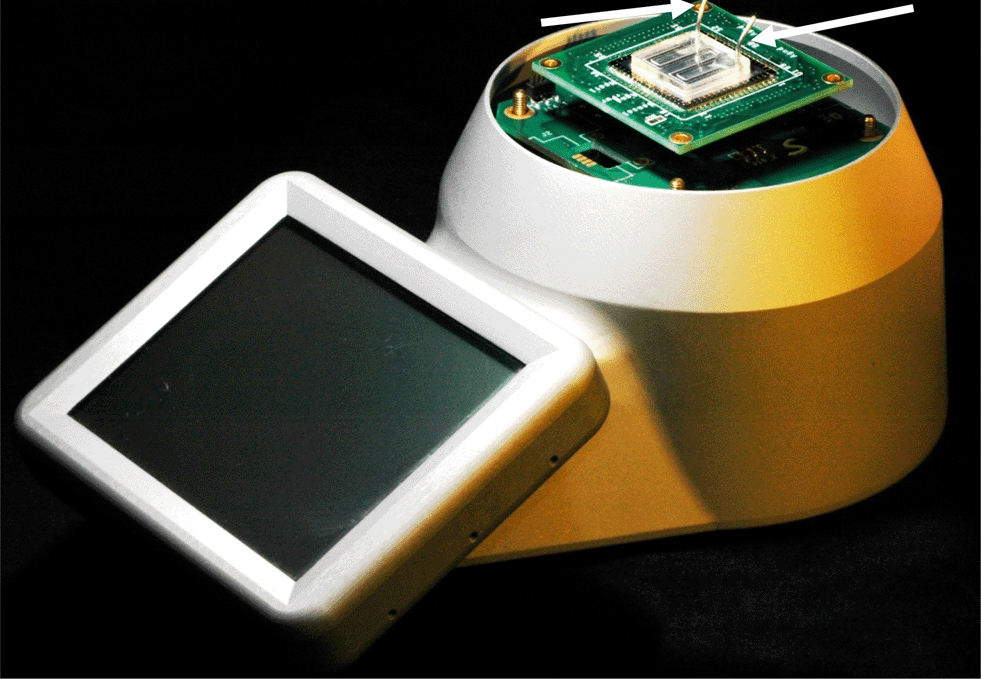 | ||
| Fig. 8 A photograph of the LOC system in configuration to test the nanowire based sensors with microfluidics channel as per the design in Fig. 6. The fluid was delivered to the system by the tubes connected to the chip through the PDMS cap as shown by the arrows. | ||
The PCB with the nanowire chip was then plugged into the LOC. The analog switches were controlled from a PC set for 5 s per measurement of a single unit. The chip was sequentially read out. The measurement of all sensors took 85 s in total (Fig. 9). As all the four channels of our oscilloscope were occupied by NW measurements, we designed the program to control the switches so that no switch was active at the start.
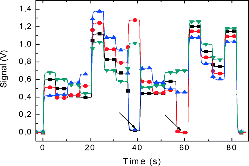 | ||
| Fig. 9 Real-time measurements taken from the 64 nanowire (NW) chip in 85 s. The NWs were clustered into 16 groups, each containing 4 NWs, and were simultaneously measured. Electrical output signal corresponding to each demultiplexer (Fig. 6d) has a different color. This is a static measurement that shows the status of all 64 NWs. We have measured 4 NWs from group 1, addressed by the demultiplexer for about 3 s, switched to group 2 etc. until all 16 groups were measured. The arrows show four defective NWs, two from group 8 and two from group 12. A buffer solution with pH 7 was inside the microchannel. | ||
We used this feature as a marker to establish the switching sequence, which can then be set for all subsequent measurements. The PCB with the soldered nanowire chip was plugged into the LOC system, and the conductivity was recorded as a function of time. During the recording, we manually covered the chip with 1 μL of pH 10 calibration buffer for 60 s and changed the buffer to pH 7 for about a minute, to be followed with pH 4 buffer. The system response to the pH value is shown in Fig. 10.
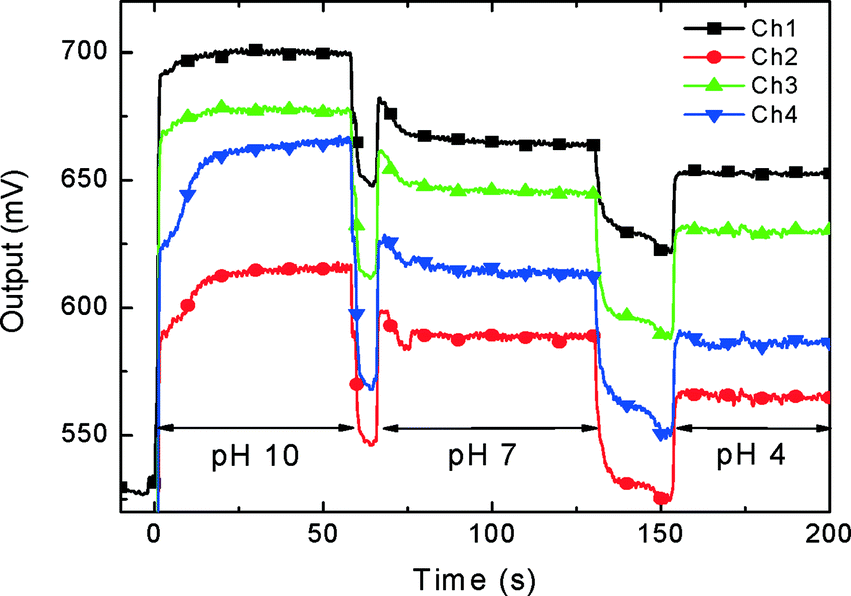 | ||
| Fig. 10 Application of the 4 nanowire sensor to detect pH variations. 1 μL of buffer solution was manually dispensed for about 60 s and removed by capillary force before the new buffer was dispensed. | ||
We also used an older device with only 4 NW sensors to test the pH of different solutions (Fig. 10) in sequence, with real-time detection.
Electrochemical detector
We used the chip as shown in Fig. 7 to demonstrate the functionality of this platform for electrochemistry applications. The chip was attached in the same way as the PCR and NW chip by soldering to the PCB. The glass substrate of this chip has a thermal conductivity about 100 times lower than silicon, and the soldering time was adapted to this.First, we measured the oxidation/reduction of ferro/ferricyanide redox couple,35 a widely-used calibration reaction to evaluate the behavior of the electrochemical sensors. We applied voltage pulses identical to the ones used in the NW measurements, while all electrochemical cells were biased with a sawtooth signal. The signal generator was connected between the I/U converter and the attenuator (Fig. 6d). The measurement was conducted by the pulse technique,35 and the lock-in amplifier automatically provided a signal derivation with respect to time. This method enabled us to directly obtain a curve similar to that obtained by differential pulse cyclic voltammetry (DPV) technique.36
In a DPV measurement, the increasing and decreasing curves should be almost identical. The difference observed in Fig. 11 could be attributed to voltammetry/pulse conditions, where pulse duration and the phase shift for each signal generator (Fig. 2) may benefit from a complete optimisation.36
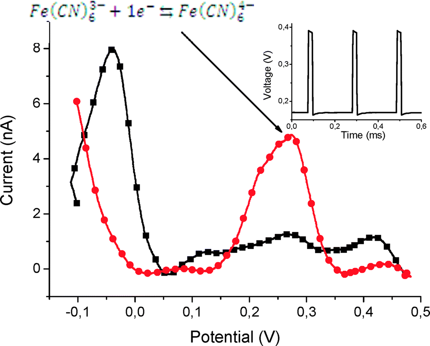 | ||
| Fig. 11 Response of an electrochemical chip to pulsed voltage. The system behavior is similar to differential pulse voltammetry. The figure shows the current when increasing (red) and decreasing (black) the potential. The curves enable the identification of the redox peaks of the ferro/ferricyanide oxidation–reduction reaction. (Inset) Details of the biasing pulses superimposed to the sawtooth signal with peak to peak amplitudes of 0.6 V, an offset of 0.2 V and a slope of 100 mV s−1. | ||
Temperature measurement
The number of channels available for temperature measurement has been increased to four in this system, using an AC biased Wheatstone bridge with a lock-in amplification technique for the signal enhancement (Fig. 12).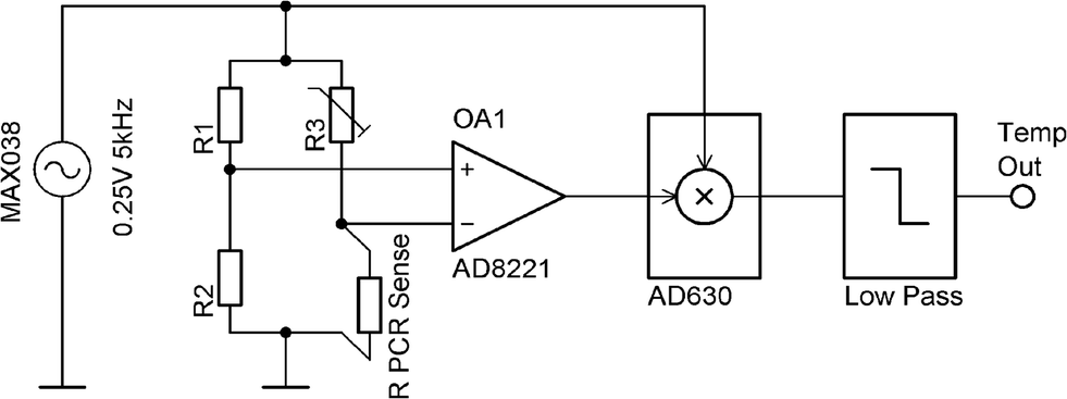 | ||
| Fig. 12 Single channel ASLOC temperature sensing used for PCR. AC powered Wheatstone bridge with lock-in based amplification technique. | ||
High voltage controller
For this LOC instrument, we have also developed a high voltage (HV) power supply controllable up to 1000 V programmed with 100 ms long pulses (Fig. 13). The HV output was loaded with 10 MΩ and 1 MΩ resistors. The load value lowers the total voltage by making the discharging faster. In the future, the designed HV system will be able to accommodate pulse width modulation, independent of the load impedance.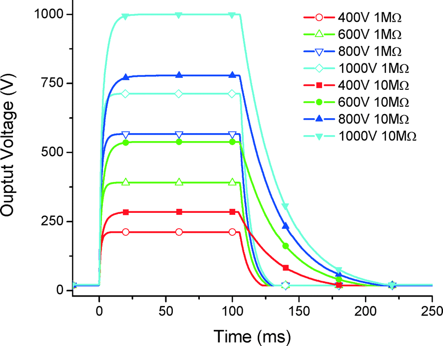 | ||
| Fig. 13 High voltage power supply with 1000 V, 800 V, 600 V and 400 V setting with two different loading resistors, 10 MΩ and 1 MΩ. It shows the load influence on the output voltage as well as on the discharging time. | ||
Conclusion
A versatile instrument platform for lab-on-a-chip devices was developed. The overall power consumption of the system is 4 W, making it a suitable candidate for the point-of-care diagnostics, field operations and primarily for educational purposes. The system can be simply changed from one application to another.We have tested two types of systems: current- and voltage-based interrogations. Taken together, they cover the majority of LOC applications currently in use or in research. In the first category, we demonstrated real-time PCR and LSPR detections, while the measurement of NWs and electrochemical cells illustrated the second. The voltage interrogation scheme specifically enables the measurements of significant arrays of sensors, here represented by 64 units, which were carried out in 85 s.
The platform presented here has the potential to open a new chapter in LOC development, as it is easily adaptable for many different applications and can be used in remote locations and for educational purposes, such as undergraduate or college teaching labs.
Acknowledgements
P. Neužil acknowledges partial financial support from the Central European Institute of Technology (CEITEC), grant number CZ.1.05/1.1.00/02.0068. C. Campos is grateful to São Paulo Research Foundation (FAPESP) for financial support, grant number 2013/06625-2. We are also grateful to L. Novák for help with measurement setups and to M. Neužilová for editing assistance.Notes and references
- A. Manz, N. Graber and H. M. Widmer, Sens. Actuators, B, 1990, 1, 244–248 CrossRef CAS.
- Á. Ríos, M. Zougagh and M. Avila, Anal. Chim. Acta, 2012, 740, 1–11 CrossRef PubMed.
- K. S. Elvira, X. C. I. Solvas, R. C. R. Wootton and A. J. Demello, Nat. Chem., 2013, 5, 905–915 CrossRef CAS PubMed.
- P. N. Nge, C. I. Rogers and A. T. Woolley, Chem. Rev., 2013, 113, 2550–2583 CAS.
- A. Kaushik, A. Vasudev, S. K. Arya, S. K. Pasha and S. Bhansali, Biosens. Bioelectron., 2014, 53, 499–512 CrossRef CAS PubMed.
- K. N. Han, C. A. Li and G. H. Seong, Annu. Rev. Anal. Chem., 2013, 6, 119–141 CrossRef CAS PubMed.
- J. Lee and S.-H. Lee, Biomed. Eng. Lett., 2013, 3, 59–66 CrossRef.
- A. P. Lewis, A. Cranny, N. R. Harris, N. G. Green, J. A. Wharton, R. J. K. Wood and K. R. Stokes, Meas. Sci. Technol., 2013, 24, 042001 CrossRef.
- Z. Yushan, C. Jacquemod and M. Sawan, 2013 IEEE International Symposium on Circuits and Systems (ISCAS), Beijing, China, 2013, 1071–1074 Search PubMed.
- J. Yang, C. Brooks, M. D. Estes, C. M. Hurth and F. Zenhausern, Forensic Sci. Int.: Genet., 2014, 8, 147–158 CrossRef CAS PubMed.
- M. Czugala, D. Maher, F. Collins, R. Burger, F. Hopfgartner, Y. Yang, J. Zhaou, J. Ducree, A. Smeaton, K. J. Fraser, F. Benito-Lopez and D. Diamond, RSC Adv., 2013, 3, 15928–15938 RSC.
- F.-E. Legiret, V. J. Sieben, E. M. S. Woodward, S. K. Abi Kaed Bey, M. C. Mowlem, D. P. Connelly and E. P. Achterberg, Talanta, 2013, 116, 382–387 CrossRef CAS PubMed.
- A. Fernández-la-Villa, D. Sánchez-Barragán, D. F. Pozo-Ayuso and M. Castaño-Álvarez, Electrophoresis, 2012, 33, 2733–2742 CrossRef PubMed.
- S. Wang, F. Inci, T. L. Chaunzwa, A. Ramanujam, A. Vasudevan, S. Subramanian, A. C. F. Ip, B. Sridharan, U. A. Gurkan and U. Demirci, Int. J. Nanomed., 2012, 7, 2591–2600 CAS.
- P. B. Lillehoj, M. C. Huang and C. M. Ho, 2013 IEEE 26th International Conference on Micro Electro Mechanical Systems (MEMS), Taipei, Taiwan, 2013, 53–56 Search PubMed.
- K. Ansari, J. Y. S. Ying, P. C. Hauser, N. F. de Rooij and I. Rodriguez, Electrophoresis, 2013, 34, 1390–1399 CrossRef CAS PubMed.
- C. Toumazou, L. M. Shepherd, S. C. Reed, G. I. Chen, A. Patel, D. M. Garner, C. J. Wang, C. P. Ou, K. Amin-Desai, P. Athanasiou, H. Bai, I. M. Brizido, B. Caldwell, D. Coomber-Alford, P. Georgiou, K. S. Jordan, J. C. Joyce, M. La Mura, D. Morley, S. Sathyavruthan, S. Temelso, R. E. Thomas and L. Zhang, Nat. Methods, 2013, 10, 641–646 CrossRef CAS PubMed.
- Y. Fintschenko, Lab Chip, 2011, 11, 3394–3400 RSC.
- M. Hemling, J. A. Crooks, P. M. Oliver, K. Brenner, J. Gilbertson, G. C. Lisensky and D. B. Weibel, J. Chem. Educ., 2013, 91, 112–115 CrossRef.
- C. W. Yang and E. T. Lagally, Methods Mol. Biol., 2013, 949, 25–40 CAS.
- A. Priye, Y. A. Hassan and V. M. Ugaz, Lab Chip, 2012, 12, 4946–4954 RSC.
- P. Neuzil, J. Pipper and T. M. Hsieh, Mol. BioSyst., 2006, 2, 292–298 RSC.
- P. Neuzil, C. Zhang, J. Pipper, S. Oh and L. Zhuo, Nucleic Acids Res., 2006, 34, e77 CrossRef PubMed.
- L. Novak, P. Neuzil, J. Pipper, Y. Zhang and S. Lee, Lab Chip, 2007, 7, 27–29 RSC.
- J. Pipper, M. Inoue, L. F. Ng, P. Neuzil, Y. Zhang and L. Novak, Nat. Med., 2007, 13, 1259–1263 CrossRef CAS PubMed.
- J. Pipper, Y. Zhang, P. Neuzil and T. M. Hsieh, Angew. Chem., Int. Ed., 2008, 47, 3900–3904 CrossRef CAS PubMed.
- P. Neuzil, L. Novak, J. Pipper, S. Lee, L. F. Ng and C. Zhang, Lab Chip, 2010, 10, 2632–2634 RSC.
- P. Neuzil and J. Reboud, Anal. Chem., 2008, 80, 6100–6103 CrossRef CAS PubMed.
- L. Novak, P. Neuzil, J. S. B. Woon and Y. Wee, IEEE Sensors 2009 Conference, Christchurch, New Zealand, 2009, 405–407 Search PubMed.
- C. A. Gaydos, B. Van Der Pol, M. Jett-Goheen, M. Barnes, N. Quinn, C. Clark, G. E. Daniel, P. B. Dixon and E. W. Hook 3rd, J. Clin. Microbiol., 2013, 51, 1666–1672 CrossRef PubMed.
- P. Neuzil, C. C. Wong and J. Reboud, Nano Lett., 2010, 10, 1248–1252 CrossRef CAS PubMed.
- Y. Cui, Q. Wei, H. Park and C. M. Lieber, Science, 2001, 293, 1289–1292 CrossRef CAS PubMed.
- G. J. Zhang, Z. H. Luo, M. J. Huang, J. J. Ang, T. G. Kang and H. Ji, Biosens. Bioelectron., 2011, 28, 459–463 CrossRef CAS PubMed.
- G. J. Zhang, G. Zhang, J. H. Chua, R. E. Chee, E. H. Wong, A. Agarwal, K. D. Buddharaju, N. Singh, Z. Gao and N. Balasubramanian, Nano Lett., 2008, 8, 1066–1070 CrossRef CAS PubMed.
- V. K. Cumyn, M. D. Fleischauer, T. D. Hatchard and J. R. Dahn, Electrochem. Solid-State Lett., 2003, 6, E15–E18 CrossRef CAS PubMed.
- K. F. Drake, R. P. Van Duyne and A. M. Bond, J. Electroanal. Chem., 1978, 89, 231–246 CrossRef CAS.
Footnote |
| † Currently at Division of Biomedical Engineering, University of Glasgow, Rankine Building, Oakfield Avenue, G12 8LT, Glasgow, UK. |
| This journal is © The Royal Society of Chemistry 2014 |