Research highlights
Šeila
Selimović
ab,
Mehmet R.
Dokmeci
ab and
Ali
Khademhosseini
*abcd
aCenter for Biomedical Engineering, Department of Medicine, Brigham and Women's Hospital, Harvard Medical School, Cambridge, Massachusetts 02139, USA. E-mail: alik@rics.bwh.harvard.edu
bHarvard-MIT Division of Health Sciences and Technology, Massachusetts Institute of Technology, Cambridge, Massachusetts 02139, USA
cWyss Institute for Biologically Inspired Engineering, Harvard University, Boston, Massachusetts 02115, USA
dWorld Premier International – Advanced Institute for Materials Research (WPI-AIMR), Tohoku University, Sendai 980-8577, Japan
First published on 17th December 2013
Long-term sample preservation on-chip
The emerging need for point-of-care lab-on-a-chip devices and diagnostic chips for use in remote areas is giving rise to new engineering challenges. In certain situations where biological samples can only be collected, but not analyzed in the field, the common procedure calls for drying and freezing of the specimens prior to their transport. The “cold chain” required to maintain the stability of the analytes and samples involves transport on dry ice as well as in freezers for medium and long term storage. This storage approach relies on a continuous power supply and can be costly and unavailable especially in remote areas.1 This limitation has been overcome with respect to pure blood samples by developing dried blood spots.2 These are small blood droplets deposited onto a wicking paper, from which they can later be eluted and recovered. Other samples, such as blood plasma or RNA, are not suitable to this drying method due to the risk of contamination and long drying times (up to several hours).The team led by Rustem Ismagilov has addressed this challenge by applying their microfluidic chip called the SlipChip to drying and archiving of biological samples.3 The SlipChip technology refers to microfluidic devices usually consisting of 2 or 3 stacked layers that can be slipped relative to each other to either establish continuous fluidic paths or to separate flow channels into several distinct units (e.g. reservoirs). These devices are fabricated from laser cut poly(methyl methacrylate) (PMMA) and poly(ethylene terephthalate) (PET) or other non-gas permeable, transparent materials. Applying the SlipChip to resolve the long-term sample storage problem meant that the device should be capable of speed-drying and storing samples for an extended period of time, ideally months. Thus, the device was modified to include a polypropylene membrane that separated the top fluidic layer containing the liquid sample from the bottom control layer, which was filled with a desiccant. A stack of these 3 layers was then sandwiched between two acrylic plates and placed in a sturdy plastic frame with gaskets to ensure that the seal between any two elements of this structure would not be compromised during transport (Fig. 1a). Additionally, the fluidic layer was covered with a pumping lid, a hollow structure which surrounded the input port. When the lid was placed on the device, the air inside was compressed. This, in turn forced the aqueous sample to move into the flow channel.
 | ||
| Fig. 1 Photographs of the empty SlipChip prior to loading (A), after loading with a green dyed plasma (B), after drying (C), and after sample rehydration (D). The original sample can be reconstituted in multiple drying–rehydration cycles. Figure adapted and reprinted with permission from the Royal Society of Chemistry from Begolo et al.3 | ||
In short, the sample (e.g. blood from a finger prick) was pipetted into the inlet port of the fluidic channel. The geometry and dimensions of the flow channel in this layer were chosen to enable a continuous flow of the sample upon activating the pumping lid (Fig. 1b). This could be accomplished regardless of the volume of the sample. For example, in case the sample volume was smaller than the volume of the fluidic channel, air got trapped inside the channel where a single slip of the device was used to evacuate the air bubble. The same slipping step ensured that two events took place: a) the flow channel within the fluidic layer was separated into multiple storage chambers or reservoirs and b) these reservoirs became exposed to the desiccant underneath through the gas-permeable membrane. Then, within a few minutes, the samples dried out, leaving the dry analyte inside the fluidic channel (Fig. 1c). While the slipping motion required to dry the sample was simple to execute, the slipping motion in the reverse direction was more difficult. This was done by incorporating a “fail-safe” element into the device holder that would prevent accidental slipping of the different layers of the chip. But, when the layers were realigned with each other, the fluidic path inside the top layer was reestablished. This design allowed a drop of water which was added to the input port to enter the entire channel and rehydrate the dry sample (Fig. 1d). Finally, the reconstituted sample could be collected with a pipette for analysis. If necessary, the entire drying–rehydration cycle could be repeated several times. The high quality of the reconstituted samples (HIV-1 RNA spiked blood plasma) was confirmed in a polymerase chain reaction (PCR) allowing comparison of the SlipChip samples with frozen samples.
The present iteration of the SlipChip is an excellent example of how innovative thinking, rather than financial means can be the key to solving major technological problems. In fact, the SlipChip helps lower the cost of medical testing in the field through reducing the cold chain infrastructure to the size of a credit-card sized plastic chip that can be mass produced. Miniaturization approaches such as the current platform are likely to enable advances in modern therapeutics and diagnostics, especially in resource-poor regions.
Wireless nanobiosensors using CMOS chips
The ubiquity of microscale technologies like CMOS (complementary metal-oxide-semiconductor), nanowires (NW), and lab-on-a-chip systems is enabling forays into low-cost, fast response, and portable devices. This is particularly valuable in making point-of-care (POC) devices, which serve as diagnostic sensors for the medical community, among others.4 The pervasive nature of wireless technology is another powerful approach that can be useful for POC applications, as it helps to minimize the local infrastructure by keeping the sensor untethered and enables data collection and analysis from a distance.In an exciting attempt, Lin and coworkers5 merged these individual technologies to develop a wireless biomolecular sensing chip suitable for disease diagnostics and therapeutics. The different elements of the sensor are shown in Fig. 2a, including the NW-based biosensor and an analog-to-digital converter (ADC) all realized on the same CMOS chip. Briefly, the attachment of a charged molecule to the nanowire sensor leads to a change in its conductivity and ultimately results in a resistance change of the biosensor. A typical analog output of the sensor in phosphate buffered saline (PBS) buffer with different pH concentrations can be seen in Fig. 2c. The limit of detection (LOD) was of the order of 10 fM to 10 pM, depending on the details of the biosensor processing, which is within the standard biosensor range. The voltage output was known to depend on the ambient temperature, which also necessitated the inclusion of a temperature sensor on chip. The circuit was designed to operate in an aqueous environment, and required protection from short circuits during operation. Thus, epoxy was used to cover the bonding pads and the connections on-chip, where the aqueous sample was confined to the area on top of the NW biosensor via the use of a plastic reservoir (Fig. 2b).
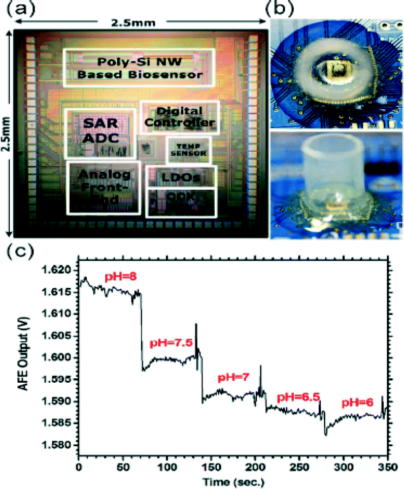 | ||
| Fig. 2 Photograph of the biosensor components on the CMOS circuitry (a) and the nanowire (NW) sensor with the attached plastic sample reservoir (b). The output of the analog front end (just before the analog-to-digital conversion) is shown for various pH solutions (c). Figure reprinted and adapted with permission from the Royal Society of Chemistry from Huang et al.5 | ||
To fabricate their biosensor, Lin et al.5 used the poly 2 layer of the CMOS process due to its lower doping level which resulted in higher sensitivity sensors. To create the polysilicon NW biosensor, the group etched the oxide layer residing on top of the poly 2 layer by using a combination of dry reactive ion etching and a wet buffered oxide etch. The polysilicon (poly-Si) NW resistors were connected in a conventional Wheatstone bridge architecture to improve not only the sensitivity but also the common-mode rejection ratio. The poly-Si NW resistors were functionalized by single stranded DNA (ssDNA). When the target DNA is bound to the probe DNA on the NW resistors, this binding process reduces the conductance of the poly-Si NW, hence increasing their resistance which is picked up by the integrated electronic circuitry. The specificity of the sensors is a result of the complementary nature of the binding DNA.
The authors were interested in studying the hepatitis B virus, hence they chose a particular ssDNA sequence that is known for its presence in all genotypes of the virus. A second DNA with only 1 base pair difference was used to validate the specificity of the sensors. Experimental data were sufficiently different in both cases to conclude that a single base-pair alteration in the probe DNA could lead to highly specific virus bonding and detection, making this platform a highly accurate choice for POC applications. Similar results were observed in detection of the cardiac biomarker, troponin I, an indicator of cardiac distress. The LOD for the hepatitis B virus DNA and the cardiac troponin biomarker was of the order of 10 fM and 10 pM, respectively. In both cases no labelling of the detected species was necessary.
The analog data obtained from the biosensor (and converted to a digital output) was wirelessly transmitted to a computer using a transceiver which was also implemented on the same CMOS chip. This capability makes the NW biosensor particularly appealing for applications in which portability is key, e.g. outside of well-equipped laboratories and in the field. To make this system even more user friendly and enhance its widespread use, it is important to develop ways to retain the DNA functionality in extreme climates (e.g. at high temperatures and humidity levels).
Attomolar DNA detection using nanotextured electrodes
The ability to detect different types of molecules in biological and environmental samples is becoming increasingly important for the development of POC devices.6 Most transistor-based sensing methods are capable of detecting concentrations down to the femtomolar (fM) scale. However, achieving attomolar (aM) sensitivity is made more difficult by the diffusion limit, as the detection of a few copies of a molecule inside a droplet can take longer than is practical (hours or longer).One approach to addressing the diffusion limit problem involves increasing the concentration of the analyte through evaporation of the solution. The research team led by Bashir and Alam adopted this approach by using electrodes in a dual role: both as a local heater to evaporate the sample droplets (synthetic DNA in a few μl of DI water) and as an impedance sensor. In particular, Ebrahimi et al.7 fabricated electrodes with microscale superhydrophobic surfaces, on which the sample droplets could be immobilized. When the microelectrodes were heated, the heat from the electrodes was transferred to the droplets causing the droplets to evaporate thereby reducing the average diffusion length of the suspended biomolecules and expediting the measurements. In addition, as the DNA became more concentrated in the solution during evaporation, more counterions were attracted to the molecules, which led to a decrease in the impedance of the sample droplet. This allowed the researchers to conduct impedance measurements utilizing only two electrodes and dispensing the commonly used reference electrode.
The Ni microelectrode structures were fabricated by electroplating using a thick photoresist mold. The protruding structures were roughly 10 μm wide, 10 μm tall, 20 μm apart and 4 mm long, a design that allowed them to support μl sized droplets. An alternating potential with a 10 mV amplitude (peak-to-peak) was applied between the anode and the cathode at a frequency of about 100 Hz (ideally, at 120 Hz) to eliminate low-frequency noise and to maximize the measurement sensitivity.
Although the electrodes had a superhydrophobic surface, it was possible to immobilize the droplets on them. This can be explained as follows: a droplet pinned on a symmetrically rough surface such as the one shown in Fig. 3a–c experiences the same interfacial tension in the two directions parallel to the edge of the protuberance, resulting in a circular contact line. Here, the droplet can easily be shifted from its equilibrium position. However, in the case of anisotropic surface topographies, such as those depicted in Fig. 3d, the droplet experiences an energy barrier perpendicular to the protuberance. This causes the droplet to remain pinned to the structure in this direction. At the same time, the interfacial tension is lower in the direction parallel to the protruding structures (there is no energy barrier that needs to be overcome), enabling the droplet to spread out in that direction. It is noteworthy to mention that as the droplet spreads out, it remains pinned to the surface and the contact line and therefore the pinned droplet surface remains unchanged, regardless of any variations in the droplet volume. This particular characteristic was exploited by the researchers, who were able to relate at any point in time the decrease in the impedance of the droplet during evaporation to the increase in the DNA concentration. In essence, each experiment provided multiple concentration measurements (each recorded at a different time), which helped gather statistically relevant data reflecting the absolute amount of DNA contained in the droplet.
 | ||
| Fig. 3 A droplet in the Cassie (a) and the Wenzel (b) state. In the first case the droplet does not fill the gaps between the protruding structures (blue), in the second case it fills the entire gap. The real contact angle of a droplet on a heterogeneous rough surface is better approximated by the Cassie model. Depending on the substrate topography, the droplet either has a circular (c) or an oval contact line (d). In (d) the non-uniform surface tension distribution leads to pinning and immobilization of the droplet. Figure reprinted with permission from the Royal Society of Chemistry from Ebrahimi et al.7 | ||
This approach allowed the researchers to quantify DNA concentrations of over 8 orders of magnitude in a single droplet, down to the aM scale. Moreover, a typical experiment was completed within 20 minutes and provided statistically significant results. Importantly, the impedance measurements of the droplet could be recorded continuously over a period of time, giving a dynamic picture of the sample, instead of only being collected as the end-point measurement. Lastly, the fact that a single set of electrodes served both as localized heaters to induce evaporation of the droplets as well as the detection platform is a major benefit of this approach. The dual use of the electrodes helps minimize the footprint of the device, reduces the external infrastructure and keeps the fabrication and operation costs low. One limitation of the presented platform lies in the lack of a species-specific measurement. For example, the sensor cannot distinguish between different biomolecules contained inside the same sample, but instead reports the impedance of the droplet as a whole. Thus, it may be prudent to couple this biosensor with a filtering element on a microfluidic device or with a labelling scheme.
References
- M. A. Dineva, L. Mahilum-Tapay and H. Lee, Analyst, 2007, 132, 1193–1199 RSC.
- M. J. Jebrail, H. Yang, J. M. Mudrik, N. M. Lafreniere, C. McRoberts, O. Y. Al-Dirbashi, L. Fisher, P. Chakraborty and A. R. Wheeler, Lab Chip, 2011, 11, 3218–3224 RSC.
- S. Begolo, F. Shen and R. F. Ismagilov, Lab Chip, 2013, 13, 4331 RSC.
- P. Yager, G. J. Domingo and J. Gerdes, Annu. Rev. Biomed. Eng., 2008, 10, 107–144 CrossRef CAS PubMed.
- C.-W. Huang, Y.-J. Huang, P.-W. Yen, H.-H. Tsai, H.-H. Liao, Y.-Z. Juang, S.-S. Lu and C.-T. Lin, Lab Chip, 2013, 13, 4451 RSC.
- D. A. Giljohann and C. A. Mirkin, Nature, 2009, 462, 461–464 CrossRef CAS PubMed.
- A. Ebrahimi, P. Dak, E. Salm, S. Dash, S. V. Garimella, R. Bashir and M. A. Alam, Lab Chip, 2013, 13, 4248 RSC.
| This journal is © The Royal Society of Chemistry 2014 |